EP0036932B1 - Sense amplifying system and memory using this system - Google Patents
Sense amplifying system and memory using this system Download PDFInfo
- Publication number
- EP0036932B1 EP0036932B1 EP81100815A EP81100815A EP0036932B1 EP 0036932 B1 EP0036932 B1 EP 0036932B1 EP 81100815 A EP81100815 A EP 81100815A EP 81100815 A EP81100815 A EP 81100815A EP 0036932 B1 EP0036932 B1 EP 0036932B1
- Authority
- EP
- European Patent Office
- Prior art keywords
- lines
- amplifying system
- memory
- cells
- coupled
- Prior art date
- Legal status (The legal status is an assumption and is not a legal conclusion. Google has not performed a legal analysis and makes no representation as to the accuracy of the status listed.)
- Expired
Links
Images

Classifications
-
- G—PHYSICS
- G11—INFORMATION STORAGE
- G11C—STATIC STORES
- G11C5/00—Details of stores covered by group G11C11/00
- G11C5/02—Disposition of storage elements, e.g. in the form of a matrix array
- G11C5/025—Geometric lay-out considerations of storage- and peripheral-blocks in a semiconductor storage device
-
- G—PHYSICS
- G11—INFORMATION STORAGE
- G11C—STATIC STORES
- G11C11/00—Digital stores characterised by the use of particular electric or magnetic storage elements; Storage elements therefor
- G11C11/21—Digital stores characterised by the use of particular electric or magnetic storage elements; Storage elements therefor using electric elements
- G11C11/34—Digital stores characterised by the use of particular electric or magnetic storage elements; Storage elements therefor using electric elements using semiconductor devices
- G11C11/40—Digital stores characterised by the use of particular electric or magnetic storage elements; Storage elements therefor using electric elements using semiconductor devices using transistors
- G11C11/401—Digital stores characterised by the use of particular electric or magnetic storage elements; Storage elements therefor using electric elements using semiconductor devices using transistors forming cells needing refreshing or charge regeneration, i.e. dynamic cells
- G11C11/4063—Auxiliary circuits, e.g. for addressing, decoding, driving, writing, sensing or timing
- G11C11/407—Auxiliary circuits, e.g. for addressing, decoding, driving, writing, sensing or timing for memory cells of the field-effect type
- G11C11/409—Read-write [R-W] circuits
- G11C11/4097—Bit-line organisation, e.g. bit-line layout, folded bit lines
Definitions
- This invention relates to integrated semiconductor memory circuits and more particularly to a sense amplifying system for memory circuits which have a very high density of small cells for storing binary digits of information.
- Integrated semiconductor memory circuits particularly those employing cells which include essentially a storage capacitor and a switch, have achieved high memory cell densities.
- One of the simplest circuits for providing small memory cells is described in U.S. Patent 3,387,286, filed July 14, 1967, by R. H. Dennard. Each of these cells described therein employs essentially only a storage capacitor and a field effect transistor acting as a switch to selectively connect the capacitor to a bit/sense line.
- U.S. Patent 4,080,590 filed March 31, 1976, by W. D. Pricer, discloses a merged charge memory produced in a unipolar technology which is provided with very small capacitor cells, each of which includes substantially only a small storage capacitor having a bit/sense line connected to one terminal of the capacitor and a word line providing a coupling to the other terminal of the capacitor.
- a direct current source of charges is produced at the surface of a semiconductor substrate and a plurality of inversion storage capacitors are formed also at the surface of the semiconductor substrate in a spaced-apart relationship from the charge source.
- Voltage pulses representing binary digits are applied to one terminal of the capacitors and the other terminal of the capacitors is coupled to the direct source of charges by the application of a word pulse to a word line.
- U.S. Patent 4,040,017, filed August 2, 1977, by H. S. Lee discloses a capacitor memory similar to that disclosed in the above-identified U.S. Patent 4,080,590, wherein the charges are produced from a charge source in the form of pulses injected into the storage capacitors rather than by utilizing a direct current source of charges.
- Semiconductor memories have generally been accessed in what is known as a two-dimensional accessing arrangement wherein a single word line controls a number of memory cells with each cell having a bit/sense line connected to input/output or control circuitry.
- the input/output or control circuitry may be coupled to more than one bit/sense line to provide certain space saving advantages which may be required for sense amplifiers when very small cells of the above described type are used.
- Such accessing arrangements are at times referred to as a 2 1/2 dimensional operation.
- U.S. Patent 4,160,275 filed on April 3, 1978, by H. S. Lee, W. D. Pricer and N. G. Vogl, Jr., discloses an accessing arrangement wherein the minimum pitch of a sense amplifier may be several times the dimension of the desired or optimum bit line pitch of a merged charge memory array by selecting at one time only a small number of cells, such as a byte, associated with a word line for writing or reading purposes.
- This invention intends to provide an improved sense amplifying system permitting more efficient utilization of the surface area of a semiconductor chip, in particular for a memory system having a high density of cells.
- this invention intends to provide an improved sense amplifying system for a memory employing minimum spacing between bit/sense lines which is capable of detecting small signals and to provide an improved sense amplifying system for a memory of the one-device cell or merged charge memory type having a very high density of cells.
- This invention further intends to provide a memory array layout using such an improved sense amplifying system.
- the sense amplifying system in-cludes first and second access or bit lines, first and second differential amplifiers with isolation means for selectively and independently coupling the amplifiers to the access lines and means for establishing a reference potential on the access lines.
- the first amplifier is used to sense the signals on the first bit line while using a reference voltage derived from the second bit line and the second amplifier arranged in tandem with the first amplifier is used to sense the signal on the second bit line while using a reference voltage derived from the first bit line.
- the first and second amplifiers are disposed preferably on one side of the array which in- cludes the first and second bit lines, while third and fourth amplifiers, similar to the first and second amplifiers, are disposed on the opposite side of the array and are coupled to third and fourth bit lines which are also a part of the array.
- this invention provides an improved sense amplifying system for a memory having a high density of cells which does not require the complex circuitry of a 2 1/2 dimensionally operated memory utilizing amplifiers shared by various cells of a word line.
- the invention is applicable for a memory having a very high density of cells which is arranged for two-dimensional operation without being limited by the pitch of the sense amplifying system.
- each sense amplifier connected to a given bit line may have a pitch equal to the pitch of four bit lines of the memory.
- Fig. 1 of the drawing shows in detail a memory which includes the sense amplifying system of the present invention.
- the memory also includes an array 10 of memory cells 12A and 12B connected to a first bit line BL1, cells 12C and 12D connected to a second bit line BL2, cells 12E and 12F connected to a third bit line BL3 and cells 12G and 12H connected to a fourth bit line BL4.
- Each of the cells is illustrated as being a one-device cell having a field effect transistor and a storage capacitor of the type disclosed in the above identified Dennard patent, but it should be understood that other types of small cells may also be used in the array 10.
- Cells 12A, 12C, 12E and 12G are also coupled to a first word line W1, with cells 12B, 12D, 12F and 12H being coupled to a second word line W2.
- Word lines W1 and W2 are connected to a word decoder and driver 14 which may be of any known appropriate type.
- a first bit line decoder 16 is connected to the first and third bit lines BL1 and BL3 and has an input/output terminal I/O
- a second bot line decoder 16' is connected to the second and fourth bit lines BL2 and BL4 and has an input/output terminal I/O'.
- the bit line decoders 16 and 16' may be of any known appropriate type and may differ from each other only in that each receives different addresses. Each of the decoders 16 and 16' may, as preferred, have one input/output terminal or as many as the number of bit lines connected to the decoder.
- a first sense amplifying system 18 having a first pair of cross coupled field effect transistor devices 20 and 22 is coupled to the first and third bit lines BL1 and BL3 through first and second isolation devices or transistors 24 and 26, respectively.
- the first sense amplifying system 18 also includes a second pair of cross coupled field effect transistor devices 28 and 30 coupled to the first and third bit lines BL1 and BL3 through third and fourth isolation devices or transistors 32 and 34, respectively, tandemly arranged with respect to the first pair of cross coupled devices 20 and 22.
- a precharging or pull up circuit 36 has a first field effect transistor 38 connected between a voltage source terminal VH and the first bit line BL1, a second field effect transistor 40 connected between the voltage source terminal VH and the third bit line BL3 and a third field effect transistor 42, acting as a voltage equalizing transistor, coupled between the first and third bit lines BL1 and BL3.
- the voltage at terminal VH may be equal to +10 volts.
- Clock circuits 44 of any known appropriate type provide pulses for operating the first sense amplifying system 18. These pulses include a control pulse A which is applied to the gate electrodes of isolation transistors 26 and 32, a control pulse B which is applied to the gate electrodes of isolation transistors 24 and 34, a strobe pulse S which is applied to a common node D between the tandemly arranged first and second pairs of cross coupled transistor devices 20, 22 and 28, 30 and a precharge pulse P which is applied to the gate electrodes of the three transistors of precharging circuit 36.
- a second sense amplifying system 46 similar to the first system 18, having a first pair of cross coupled field effect transistor devices 48 and 50 is coupled to the second and fourth bit lines BL2 and BL4 through first and second isolation devices or transistors 52 and 54, respectively.
- the second sense amplifying system 46 also includes a second pair of cross coupled field effect transistor devices 56 and 58 coupled to the second and fourth bit lines BL2 and BL4 through third and fourth isolation devices or transistors 60 and 62, respectively, each of the isolation devices being preferably field effect transistors.
- a precharging or pull up circuit 64 has a first field effect transistor 66 connected between the voltage source terminal VH and the second bit line BL2, a second field effect transistor 68 connected between the voltage source terminal VH and the fourth bit line BL4 and a third field effect transistor 70, acting as a voltage equalizing transistor, coupled between the second and fourth bit lines BL2 and BL4.
- Control pulse A from the clocking circuits 44 is applied to the gate electrodes of isolation transistors 54 and 60, control pulse B is applied to the gate electrodes of isolation transistors 52 and 62, strobe pulse S is applied to a common node D between the tandemly arranged first and second pairs of cross coupled transistor devices 48, 50 and 56, 58 and precharge pulse P is applied to the gate electrodes of the three transistors of the precharging circuit 64.
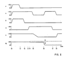
- a pulse program which may be used to operate the memory of Fig. 1 is indicated in Fig. 2 of the drawings.
- the pulses indicated in Fig. 2 include the control pulses A and B, strobe pulse S and precharge pulse P, along with a word line pulse W which is applied selectively to word lines W1 and W2 and a signal voltage BL which may be produced on the bit lines BL1, BL2, BL3 and BL4 during a reading or signal sensing operation.
- precharge pulse P is applied at time tO to precharging circuit 36 to precharge bit lines BL1 and BL3 to voltage VH equal to +10 volts.
- control pulse A is applied to transistors 26 and 32 to also charge nodes E and F to +10 volts and control pulse B is applied to transistors 24 and 34 to likewise charge nodes G and H to +10 volts, while strobe pulse S, applied to node D, is held at +10 volts.
- first and third bit lines BL1 and BL3 and nodes D, E, F, G and H are all charged to +10 volts.
- precharge pulse P is turned off, isolating the first and third bit lines BL1 and BL3 from the voltage source terminal VH and from each other.
- control pulse B is turned off to isolate node G from the first bit line BL1 and to isolate node H from the third bit line BL3, providing at node G a reference voltage for the first pair of cross coupled transistors 20, 22 and at node H a reference voltage for the second pair of cross coupled transistors 28, 30.
- the word pulse W is applied from 0'rd line W2 to the one-device cells 12B and 12F in a known manner to apply the signals stored in these cells 12B and 12F to the charged bit lines BL1 and BL3, respectively.
- the voltage on that bit line will decrease at time t4, as indicated in the solid curve BL, representing a stored "0" digit of binary information, but if charge is not withdrawn from the bit line, the voltage may rise at time t4, as indicated in the dashed curve BL, representing a stored "1" digit of binary information.
- bit lines BL1 and BL3 representing either a "0" digit or a "1" digit, is applied from the first bit line BL1 to node F of the second pair of cross coupled transistor devices 28 and 30 through transistor 32 and from the third bit line BL3 to node E of the first pair of cross coupled transistor devices 20 and 22 through transistor 26.
- the first pair of cross coupled transistor devices 20 and 22 may now act as an amplifying latch or differential amplifier for the signal voltage being applied from the third bit line BL3 to node E, while the voltage at node G acts as the reference voltage.
- the second pair of cross coupled transistor devices 28 and 30 may now act as an amplifying latch or differential amplifier for the signal voltage being applied from the first bit line BL1 to node F, while the voltage at node H acts as the reference voltage.
- control pulse A is turned off at time t5, turning off transistors 26 and 32, to isolate nodes E and F from the relatively high capacitance bit lines BL3 and BL1, respectively. Also at time t5, the strobe pulse S is gradually turned off to pull down node D to complete the amplification of the signals in the amplifiers 20, 22 and 28, 30. At time t6, control pulse A is again turned on to couple the amplified signal on node E to the third bit line BL3 and to couple the amplified signal on node F to the first bit line BL1.
- the amplified signals on bit lines BL1 and BL3 may now be fed through the bit line decoder 16 to the input/output terminal I/0 and may also be used to restore the information in cells 12B and 12F.
- curve BL of Fig. 2 of the drawings at time t6, with a "0" having been stored in a sensed cell, the voltage on the bit line to which that cell is coupled drops rapidly, discharging through the conductive transistor device of the pair of cross coupled transistor devices.
- the word pulse W is turned off, and at time t8 the control pulse A is turned off and the strobe pulse turned on to complete the reading operation.
- cells 12A and 12E may also be read out by the sense amplifying system 18 in the same manner as described hereinabove in connection with the sensing of cells 12B and 12F except that the word pulse W is applied to the word line W1 instead of to word line W2.
- the array 10 may have 128 or more word lines, if desired.
- each sense amplifying system may have a pitch equal to the pitch of four bit lines of the memory by locating one system coupled to two bit lines on one side of a memory array and locating a second system coupled to two other bit lines of the array on the opposite side thereof.
- bit lines become directly accessible for writing, switching noises are mitigated or eliminated and read modify write cycles of operation are more readily performed.
Description
- This invention relates to integrated semiconductor memory circuits and more particularly to a sense amplifying system for memory circuits which have a very high density of small cells for storing binary digits of information.
- Integrated semiconductor memory circuits, particularly those employing cells which include essentially a storage capacitor and a switch, have achieved high memory cell densities. One of the simplest circuits for providing small memory cells is described in U.S. Patent 3,387,286, filed July 14, 1967, by R. H. Dennard. Each of these cells described therein employs essentially only a storage capacitor and a field effect transistor acting as a switch to selectively connect the capacitor to a bit/sense line. U.S. Patents 3,811,076 by W. M. Smith and 3,841,926 by R. H. Garnache and W. M. Smith, both filed January 2 1973, disclose a one-device field effect transistor memory cell of the type described in the above-identified Dennard patent which is made very small by utilizing a layer of doped polycrystalline silicon separated by a dielectric medium disposed on the surface of a semiconductor substrate for forming a storage capacitor.
- U.S. Patent 3,979,734, filed June 16, 1975, by W. D. Pricer and J. E. Selleck, describes a memory array made of small cells which employ storage capacitors and bipolar transistors. In this array, each storage capacitor of these cells has simply one capacitor terminal or plate connected to a separate bit/sense line while selected cells forming a word are simultaneously accessed by utilizing a word pulse for coupling to the other terminal or plate of the storage capacitors of that word.
- U.S. Patent 4,080,590, filed March 31, 1976, by W. D. Pricer, discloses a merged charge memory produced in a unipolar technology which is provided with very small capacitor cells, each of which includes substantially only a small storage capacitor having a bit/sense line connected to one terminal of the capacitor and a word line providing a coupling to the other terminal of the capacitor. In an embodiment of that invention, a direct current source of charges is produced at the surface of a semiconductor substrate and a plurality of inversion storage capacitors are formed also at the surface of the semiconductor substrate in a spaced-apart relationship from the charge source. Voltage pulses representing binary digits are applied to one terminal of the capacitors and the other terminal of the capacitors is coupled to the direct source of charges by the application of a word pulse to a word line.
- U.S. Patent 4,040,017, filed August 2, 1977, by H. S. Lee, discloses a capacitor memory similar to that disclosed in the above-identified U.S. Patent 4,080,590, wherein the charges are produced from a charge source in the form of pulses injected into the storage capacitors rather than by utilizing a direct current source of charges.
- Semiconductor memories have generally been accessed in what is known as a two-dimensional accessing arrangement wherein a single word line controls a number of memory cells with each cell having a bit/sense line connected to input/output or control circuitry. However, it is known in the prior art that the input/output or control circuitry may be coupled to more than one bit/sense line to provide certain space saving advantages which may be required for sense amplifiers when very small cells of the above described type are used. Such accessing arrangements are at times referred to as a 2 1/2 dimensional operation.
- U.S. Patent 4,160,275, filed on April 3, 1978, by H. S. Lee, W. D. Pricer and N. G. Vogl, Jr., discloses an accessing arrangement wherein the minimum pitch of a sense amplifier may be several times the dimension of the desired or optimum bit line pitch of a merged charge memory array by selecting at one time only a small number of cells, such as a byte, associated with a word line for writing or reading purposes.
- U.S. Patent 4,061,954, filed in December 6, 1977, by R. J. Proebsting and P. R. Schroeder, discloses a sense amplifying system with a single differential amplifier coupled by parallel isolation transistors to a true and a complement digit line. The parallel isolation transistors simultaneously connect the digit lines to both inputs of the amplifier. However, this design requires dummy cells which have to be connected to one of the digit lines when the other digit line is addressed.
- The problem encountered with prior art sense amplifiers when applied to high density memories is twofold. First, the electrical performance of the sense amplifiers, e.g. signal-to-noise ratio and amplification, has to be improved in order to compensate for the lower output of smaller memories and their higher signal-to-noise ratios. Second, the total area occupied by the sense amplifiers has to be decreased or their placement has to be improved such that at least the memory cells can be arranged very densily.
- This invention intends to provide an improved sense amplifying system permitting more efficient utilization of the surface area of a semiconductor chip, in particular for a memory system having a high density of cells.
- Also, this invention intends to provide an improved sense amplifying system for a memory employing minimum spacing between bit/sense lines which is capable of detecting small signals and to provide an improved sense amplifying system for a memory of the one-device cell or merged charge memory type having a very high density of cells. This invention further intends to provide a memory array layout using such an improved sense amplifying system.
- This invention, as claimed, provides this improved sense amplifying system. Essentially, it includes an amplifying and latching device, an isolating device for the amplifying and latching device and a distinct pull up device. More specifically, the sense amplifying system in-cludes first and second access or bit lines, first and second differential amplifiers with isolation means for selectively and independently coupling the amplifiers to the access lines and means for establishing a reference potential on the access lines. The first amplifier is used to sense the signals on the first bit line while using a reference voltage derived from the second bit line and the second amplifier arranged in tandem with the first amplifier is used to sense the signal on the second bit line while using a reference voltage derived from the first bit line. In a memory array according to the invention, the first and second amplifiers are disposed preferably on one side of the array which in- cludes the first and second bit lines, while third and fourth amplifiers, similar to the first and second amplifiers, are disposed on the opposite side of the array and are coupled to third and fourth bit lines which are also a part of the array.
- Thus, this invention provides an improved sense amplifying system for a memory having a high density of cells which does not require the complex circuitry of a 2 1/2 dimensionally operated memory utilizing amplifiers shared by various cells of a word line.
- Also, the invention is applicable for a memory having a very high density of cells which is arranged for two-dimensional operation without being limited by the pitch of the sense amplifying system.
- Further, it provides a system for a two- dimensionally operated memory wherein each sense amplifier connected to a given bit line may have a pitch equal to the pitch of four bit lines of the memory.
- The foregoing and other objects, features and advantages of the invention will be apparent from the following more particular description of the preferred embodiment of the invention, as illustrated in the accompanying drawings, in which:
- Fig. 1 is a circuit diagram of an embodiment of a sense amplifying system of the present invention; and
- Fig. 2 is a pulse program which may be used to operate the sense amplifying system of the invention as illustrated in Fig. 1.
- Fig. 1 of the drawing shows in detail a memory which includes the sense amplifying system of the present invention. The memory also includes an
array 10 ofmemory cells 12A and 12B connected to a first bit line BL1, cells 12C and 12D connected to a second bit line BL2,cells 12E and 12F connected to a third bit line BL3 andcells 12G and 12H connected to a fourth bit line BL4. Each of the cells is illustrated as being a one-device cell having a field effect transistor and a storage capacitor of the type disclosed in the above identified Dennard patent, but it should be understood that other types of small cells may also be used in thearray 10.Cells cells 12B, 12D, 12F and 12H being coupled to a second word line W2. Word lines W1 and W2 are connected to a word decoder anddriver 14 which may be of any known appropriate type. A firstbit line decoder 16 is connected to the first and third bit lines BL1 and BL3 and has an input/output terminal I/O, and a second bot line decoder 16' is connected to the second and fourth bit lines BL2 and BL4 and has an input/output terminal I/O'. - The
bit line decoders 16 and 16' may be of any known appropriate type and may differ from each other only in that each receives different addresses. Each of thedecoders 16 and 16' may, as preferred, have one input/output terminal or as many as the number of bit lines connected to the decoder. - A first
sense amplifying system 18 having a first pair of cross coupled fieldeffect transistor devices transistors 24 and 26, respectively. The firstsense amplifying system 18 also includes a second pair of cross coupled fieldeffect transistor devices transistors devices circuit 36 has a firstfield effect transistor 38 connected between a voltage source terminal VH and the first bit line BL1, a second field effect transistor 40 connected between the voltage source terminal VH and the third bit line BL3 and a thirdfield effect transistor 42, acting as a voltage equalizing transistor, coupled between the first and third bit lines BL1 and BL3. The voltage at terminal VH may be equal to +10 volts. -
Clock circuits 44 of any known appropriate type provide pulses for operating the firstsense amplifying system 18. These pulses include a control pulse A which is applied to the gate electrodes ofisolation transistors isolation transistors 24 and 34, a strobe pulse S which is applied to a common node D between the tandemly arranged first and second pairs of cross coupledtransistor devices circuit 36. - A second
sense amplifying system 46, similar to thefirst system 18, having a first pair of cross coupled fieldeffect transistor devices 48 and 50 is coupled to the second and fourth bit lines BL2 and BL4 through first and second isolation devices ortransistors sense amplifying system 46 also includes a second pair of cross coupled fieldeffect transistor devices transistors - The first and second pairs of cross coupled
devices circuit 64 has a firstfield effect transistor 66 connected between the voltage source terminal VH and the second bit line BL2, a secondfield effect transistor 68 connected between the voltage source terminal VH and the fourth bit line BL4 and a thirdfield effect transistor 70, acting as a voltage equalizing transistor, coupled between the second and fourth bit lines BL2 and BL4. - Control pulse A from the
clocking circuits 44 is applied to the gate electrodes ofisolation transistors isolation transistors transistor devices precharging circuit 64. - A pulse program which may be used to operate the memory of Fig. 1 is indicated in Fig. 2 of the drawings. The pulses indicated in Fig. 2 include the control pulses A and B, strobe pulse S and precharge pulse P, along with a word line pulse W which is applied selectively to word lines W1 and W2 and a signal voltage BL which may be produced on the bit lines BL1, BL2, BL3 and BL4 during a reading or signal sensing operation.
- To read information from, e.g., cell 12B coupled to the first bit line BL1 and cell 12F coupled to the third bit line BL3 in the
array 10, precharge pulse P is applied at time tO to prechargingcircuit 36 to precharge bit lines BL1 and BL3 to voltage VH equal to +10 volts. Simultaneously, control pulse A is applied totransistors transistors 24 and 34 to likewise charge nodes G and H to +10 volts, while strobe pulse S, applied to node D, is held at +10 volts. Thus, first and third bit lines BL1 and BL3 and nodes D, E, F, G and H are all charged to +10 volts. At time t1, precharge pulse P is turned off, isolating the first and third bit lines BL1 and BL3 from the voltage source terminal VH and from each other. At time t2, control pulse B is turned off to isolate node G from the first bit line BL1 and to isolate node H from the third bit line BL3, providing at node G a reference voltage for the first pair of cross coupledtransistors transistors transistor devices transistor 32 and from the third bit line BL3 to node E of the first pair of cross coupledtransistor devices transistor 26. Accordingly, it can be seen that the first pair of cross coupledtransistor devices transistor devices - To amplify the signals now stored on nodes E and F, the control pulse A is turned off at time t5, turning off
transistors amplifiers bit line decoder 16 to the input/output terminal I/0 and may also be used to restore the information in cells 12B and 12F. As can be seen in curve BL of Fig. 2 of the drawings, at time t6, with a "0" having been stored in a sensed cell, the voltage on the bit line to which that cell is coupled drops rapidly, discharging through the conductive transistor device of the pair of cross coupled transistor devices. - At time t7, with information restored in the sensed cells, the word pulse W is turned off, and at time t8 the control pulse A is turned off and the strobe pulse turned on to complete the reading operation.
- As is well known, to write new information into the cells 12B and 12F, data is fed from the input/output terminal I/O through the
bit line decoder 16 to the appropriate amplifying latches 28, 30 and 20, 22, respectively, before being stored in these cells. - Of course,
cells sense amplifying system 18 in the same manner as described hereinabove in connection with the sensing of cells 12B and 12F except that the word pulse W is applied to the word line W1 instead of to word line W2. - It can be seen that in the same manner the cells 12C and 12D coupled to the second bit line BL2 are sensed by the amplifying
latch cells 12G and 12H coupled to the fourth bit line BL4 are sensed by the amplifyinglatch 48, 50. - Although only two cells are illustrated as being connected to a bit line, it should be understood that many more cells, e.g., 128 cells, may be associated with each bit line. Furthermore, the
array 10 may have 128 or more word lines, if desired. - Accordingly, it should be noted that a sense amplifying system has been provided for a two dimensionally operated memory having very small, closely packed cells wherein each sense amplifying system may have a pitch equal to the pitch of four bit lines of the memory by locating one system coupled to two bit lines on one side of a memory array and locating a second system coupled to two other bit lines of the array on the opposite side thereof.
- It should also be noted that by connecting the sence amplifying system to the outside or edges of an array rather than locating it in the middle of the array, the bit lines become directly accessible for writing, switching noises are mitigated or eliminated and read modify write cycles of operation are more readily performed.
Claims (6)
Applications Claiming Priority (2)
| Application Number | Priority Date | Filing Date | Title |
|---|---|---|---|
| US134259 | 1980-03-26 | ||
| US06/134,259 US4287576A (en) | 1980-03-26 | 1980-03-26 | Sense amplifying system for memories with small cells |
Publications (3)
| Publication Number | Publication Date |
|---|---|
| EP0036932A2 EP0036932A2 (en) | 1981-10-07 |
| EP0036932A3 EP0036932A3 (en) | 1981-10-21 |
| EP0036932B1 true EP0036932B1 (en) | 1983-12-28 |
Family
ID=22462513
Family Applications (1)
| Application Number | Title | Priority Date | Filing Date |
|---|---|---|---|
| EP81100815A Expired EP0036932B1 (en) | 1980-03-26 | 1981-02-05 | Sense amplifying system and memory using this system |
Country Status (4)
| Country | Link |
|---|---|
| US (1) | US4287576A (en) |
| EP (1) | EP0036932B1 (en) |
| JP (1) | JPS594788B2 (en) |
| DE (1) | DE3161720D1 (en) |
Families Citing this family (10)
| Publication number | Priority date | Publication date | Assignee | Title |
|---|---|---|---|---|
| JPS57208691A (en) * | 1981-06-15 | 1982-12-21 | Mitsubishi Electric Corp | Semiconductor memory |
| US4445201A (en) * | 1981-11-30 | 1984-04-24 | International Business Machines Corporation | Simple amplifying system for a dense memory array |
| JPS58147884A (en) * | 1982-02-26 | 1983-09-02 | Toshiba Corp | Dynamic type semiconductor storage device |
| JPS6150284A (en) * | 1984-08-17 | 1986-03-12 | Mitsubishi Electric Corp | Driving method of shared sense amplifier circuit |
| US4730280A (en) * | 1984-11-20 | 1988-03-08 | Fujitsu Limited | Semiconductor memory device having sense amplifiers with different driving abilities |
| US4791616A (en) * | 1985-07-10 | 1988-12-13 | Fujitsu Limited | Semiconductor memory device |
| US4807195A (en) * | 1987-05-18 | 1989-02-21 | International Business Machines Corporation | Apparatus and method for providing a dual sense amplifier with divided bit line isolation |
| US4829476A (en) * | 1987-07-28 | 1989-05-09 | Honeywell Inc. | Differential magnetoresistive memory sensing |
| KR910009444B1 (en) * | 1988-12-20 | 1991-11-16 | 삼성전자 주식회사 | Semiconductor memory device |
| EP0479170B1 (en) * | 1990-09-29 | 1996-08-21 | Nec Corporation | Semiconductor memory device having low-noise sense structure |
Family Cites Families (19)
| Publication number | Priority date | Publication date | Assignee | Title |
|---|---|---|---|---|
| US3387286A (en) * | 1967-07-14 | 1968-06-04 | Ibm | Field-effect transistor memory |
| US3811076A (en) * | 1973-01-02 | 1974-05-14 | Ibm | Field effect transistor integrated circuit and memory |
| US3841926A (en) * | 1973-01-02 | 1974-10-15 | Ibm | Integrated circuit fabrication process |
| US3909808A (en) * | 1974-12-23 | 1975-09-30 | Ibm | Minimum pitch mosfet decoder circuit configuration |
| JPS5539073B2 (en) * | 1974-12-25 | 1980-10-08 | ||
| JPS51113545A (en) * | 1975-03-31 | 1976-10-06 | Hitachi Ltd | Memory |
| US3979734A (en) * | 1975-06-16 | 1976-09-07 | International Business Machines Corporation | Multiple element charge storage memory cell |
| US4025907A (en) * | 1975-07-10 | 1977-05-24 | Burroughs Corporation | Interlaced memory matrix array having single transistor cells |
| DE2557165C3 (en) * | 1975-12-18 | 1979-01-18 | Siemens Ag, 1000 Berlin Und 8000 Muenchen | Decoder circuit and its arrangement for integration on a semiconductor module |
| US4156938A (en) * | 1975-12-29 | 1979-05-29 | Mostek Corporation | MOSFET Memory chip with single decoder and bi-level interconnect lines |
| US4061999A (en) * | 1975-12-29 | 1977-12-06 | Mostek Corporation | Dynamic random access memory system |
| US4040017A (en) * | 1976-03-31 | 1977-08-02 | International Business Machines Corporation | Injected charge capacitor memory |
| US4080590A (en) * | 1976-03-31 | 1978-03-21 | International Business Machines Corporation | Capacitor storage memory |
| US4045783A (en) * | 1976-04-12 | 1977-08-30 | Standard Microsystems Corporation | Mos one transistor cell ram having divided and balanced bit lines, coupled by regenerative flip-flop sense amplifiers, and balanced access circuitry |
| DE2647394C2 (en) * | 1976-10-20 | 1978-11-16 | Siemens Ag, 1000 Berlin Und 8000 Muenchen | MOS semiconductor memory device |
| JPS53144232A (en) * | 1977-04-28 | 1978-12-15 | Toshiba Corp | Sensor circuit for multi-value signal charge transfer device |
| DE2746336A1 (en) * | 1977-10-14 | 1979-04-19 | Siemens Ag | Dynamic semiconductor memory of matrix type - has single cell units with flip=flop read-write stages which relate to group of memory cells |
| US4160275A (en) * | 1978-04-03 | 1979-07-03 | International Business Machines Corporation | Accessing arrangement for memories with small cells |
| DE2919166C2 (en) * | 1978-05-12 | 1986-01-02 | Nippon Electric Co., Ltd., Tokio/Tokyo | Storage device |
-
1980
- 1980-03-26 US US06/134,259 patent/US4287576A/en not_active Expired - Lifetime
-
1981
- 1981-02-05 DE DE8181100815T patent/DE3161720D1/en not_active Expired
- 1981-02-05 EP EP81100815A patent/EP0036932B1/en not_active Expired
- 1981-03-06 JP JP56031446A patent/JPS594788B2/en not_active Expired
Also Published As
| Publication number | Publication date |
|---|---|
| US4287576A (en) | 1981-09-01 |
| JPS594788B2 (en) | 1984-01-31 |
| EP0036932A2 (en) | 1981-10-07 |
| DE3161720D1 (en) | 1984-02-02 |
| EP0036932A3 (en) | 1981-10-21 |
| JPS56140589A (en) | 1981-11-02 |
Similar Documents
| Publication | Publication Date | Title |
|---|---|---|
| US4367540A (en) | Dynamic memory with an interchangeable pair of data lines and sense amplifiers | |
| EP0068645B1 (en) | A semiconductor device | |
| US4954992A (en) | Random access memory having separate read out and write in bus lines for reduced access time and operating method therefor | |
| KR960002819B1 (en) | Semiconductor memory device | |
| EP0061289B1 (en) | Dynamic type semiconductor monolithic memory | |
| US4125878A (en) | Memory circuit | |
| JPH08203266A (en) | Ferroelectric memory device | |
| JPH057796B2 (en) | ||
| US4943952A (en) | Semiconductor memory circuit with improved bit lane precharge circuit | |
| EP0323172A2 (en) | Dynamic random access memories having shared sensing amplifiers | |
| US4031522A (en) | Ultra high sensitivity sense amplifier for memories employing single transistor cells | |
| EP0185451B1 (en) | Semiconductor memory device with sense amplifiers | |
| US4086662A (en) | Memory system with read/write control lines | |
| US4445201A (en) | Simple amplifying system for a dense memory array | |
| EP0264929A2 (en) | Semiconductor memory device with improved bit line arrangement | |
| US5299157A (en) | Semiconductor memories with serial sensing scheme | |
| EP0068116B1 (en) | Memory array | |
| US5361233A (en) | Semiconductor memory apparatus | |
| US4160275A (en) | Accessing arrangement for memories with small cells | |
| EP0036932B1 (en) | Sense amplifying system and memory using this system | |
| US4520466A (en) | Dynamic random access memory | |
| US6297985B1 (en) | Cell block structure of nonvolatile ferroelectric memory | |
| EP0186745A2 (en) | Memory array | |
| US5835403A (en) | Multiplication of storage capacitance in memory cells by using the Miller effect | |
| US5710738A (en) | Low power dynamic random access memory |
Legal Events
| Date | Code | Title | Description |
|---|---|---|---|
| PUAI | Public reference made under article 153(3) epc to a published international application that has entered the european phase |
Free format text: ORIGINAL CODE: 0009012 |
|
| PUAL | Search report despatched |
Free format text: ORIGINAL CODE: 0009013 |
|
| AK | Designated contracting states |
Designated state(s): DE FR GB |
|
| AK | Designated contracting states |
Designated state(s): DE FR GB |
|
| 17P | Request for examination filed |
Effective date: 19811020 |
|
| GRAA | (expected) grant |
Free format text: ORIGINAL CODE: 0009210 |
|
| AK | Designated contracting states |
Designated state(s): DE FR GB |
|
| REF | Corresponds to: |
Ref document number: 3161720 Country of ref document: DE Date of ref document: 19840202 |
|
| ET | Fr: translation filed | ||
| PLBE | No opposition filed within time limit |
Free format text: ORIGINAL CODE: 0009261 |
|
| STAA | Information on the status of an ep patent application or granted ep patent |
Free format text: STATUS: NO OPPOSITION FILED WITHIN TIME LIMIT |
|
| 26N | No opposition filed | ||
| PGFP | Annual fee paid to national office [announced via postgrant information from national office to epo] |
Ref country code: GB Payment date: 19910118 Year of fee payment: 11 |
|
| PGFP | Annual fee paid to national office [announced via postgrant information from national office to epo] |
Ref country code: DE Payment date: 19910204 Year of fee payment: 11 |
|
| PGFP | Annual fee paid to national office [announced via postgrant information from national office to epo] |
Ref country code: FR Payment date: 19920124 Year of fee payment: 12 |
|
| PG25 | Lapsed in a contracting state [announced via postgrant information from national office to epo] |
Ref country code: GB Effective date: 19920205 |
|
| GBPC | Gb: european patent ceased through non-payment of renewal fee | ||
| PG25 | Lapsed in a contracting state [announced via postgrant information from national office to epo] |
Ref country code: DE Effective date: 19921103 |
|
| PG25 | Lapsed in a contracting state [announced via postgrant information from national office to epo] |
Ref country code: FR Effective date: 19931029 |
|
| REG | Reference to a national code |
Ref country code: FR Ref legal event code: ST |