EP0035720B1 - Apparatus for inspecting an object by light - Google Patents
Apparatus for inspecting an object by light Download PDFInfo
- Publication number
- EP0035720B1 EP0035720B1 EP81101449A EP81101449A EP0035720B1 EP 0035720 B1 EP0035720 B1 EP 0035720B1 EP 81101449 A EP81101449 A EP 81101449A EP 81101449 A EP81101449 A EP 81101449A EP 0035720 B1 EP0035720 B1 EP 0035720B1
- Authority
- EP
- European Patent Office
- Prior art keywords
- datum
- fourier transform
- order
- size
- variation
- Prior art date
- Legal status (The legal status is an assumption and is not a legal conclusion. Google has not performed a legal analysis and makes no representation as to the accuracy of the status listed.)
- Expired
Links
Images


Classifications
-
- G—PHYSICS
- G01—MEASURING; TESTING
- G01B—MEASURING LENGTH, THICKNESS OR SIMILAR LINEAR DIMENSIONS; MEASURING ANGLES; MEASURING AREAS; MEASURING IRREGULARITIES OF SURFACES OR CONTOURS
- G01B11/00—Measuring arrangements characterised by the use of optical techniques
- G01B11/02—Measuring arrangements characterised by the use of optical techniques for measuring length, width or thickness
Definitions
- This invention relates to an apparatus for inspecting an object by light and particularly to a pattern inspecting apparatus for measuring the average size of fundamental patterns substantially regularly arranged in a body or object to be inspected.
- Document US-A-3 954 337 discloses an apparatus for determining the average size of apertures in an apertured member.
- This apparatus includes a detector which is positioned to receive two adjacent light fringes on two photocells, respectively. These fringes 106a and 106b correspond to signals V z and V x' respectively.
- the average aperture width b is obtained from the relation. where k, Vy and m are values for each type of mask or other apertured member.
- the apparatus disclosed in this document requires two independent sensors for these signals and the ratio Vx/Vz is used for determining the average width b.
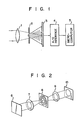
- Figs. 1 and 2 Systems for measuring the average size fundamental patterns as shown in Figs. 1 and 2 are previously known.
- the system shown in Fig. 1 is provided by Recognition Systems Inc., U.S.A., and called MAME system.
- a body 2 having an opening or aperture is illuminated by a laser or coherent light beam through a Fourier transform lens 1, and the Fourier spectrum of the body, obtained by illumination thereof through the lens, is detected by a photodiode array 3.
- the output of the diode array 3 is coupled through an A/D converter (interface) 4 to a microcomputer 5.
- the input datum which is a Fourier transform pattern image datum is processed to obtain its autocorrelation distribution. From this autocorrelation distribution the opening or aperture size of the body 2 can be determined with high precision.
- the system shown in Fig. 2 is for precisely measuring the diameter of a circular opening or aperture.
- an inspection pattern 6, obtained by laser beam irradiation is coupled through a Fourier transform lens 7 to a filter 8 disposed on the Fourier transform conversion plane, and the filter output is coupled through another Fourier transform lens 9 for photoelectric measurement on an output plane 10 to determine the aperture diameter (A. L. Flam- holz et al, IBM, J. Res. Develop. 1973, p. 509).
- the size of a single aperture (or fundamental pattern) can be measured with high precision.
- considerable time is required for the measurement, because the sizes of the individual fundamental patterns have to be measured one after another before calculation of the average value.
- the invention is intended in the light of the above, and its object is to provide an apparatus for inspecting average size of fundamental patterns at high speed and with high precision.
- an apparatus for inspecting an object by light the object having a pattern of regularly arranged units or fundamental patterns
- the apparatus comprising Fourier transform means for forming a Fourier transform pattern of the object, and processor means for determining the size of the fundamental patterns contained in the object from the Fourier transform pattern, said Fourier transform means including a Fourier transformer for providing output data corresponding to a Fourier transform pattern image of a given region of the object containing the regularly arrayed fundamental patterns
- said apparatus for inspecting an object includes an extractor responsive to the output data of said Fourier transformer for extracting a single specific datum representing a spatial frequency component of the order n from the output data, the magnitude of the order n component changing with variation of the size of fundamental patterns
- said processor means includes first means associated with said extractor for determining the average size of fundamental patterns on the given region corresponding to the single specific datum; and the order n spatial frequency component is so selected that the rate of change or the differential coefficient of the magnitude of the order n component with respect
- a single spatial frequency component is used for detecting the envelope pattern change and for determining the average size of the fundamental patterns.
- the invention is predicated on the fact that with a Fourier transform pattern image of an object having regularly arranged fundamental patterns the light intensity distribution of the spatial frequency components or diffracted light components (which is hereinafter referred to as an envelope pattern) changes with the size of the fundamental patterns.
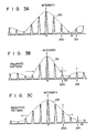
- Fig. 3A shows the Fourier spectrum of an object having regularly arrayed fundamental patterns.
- the ordinate is taken for the light intensity
- the abscissa is taken for the spatial frequency (i.e., diffraction order).
- the peaks of the light intensity are referred to as diffraction components of order n (n being 0, 1, 2,...), and the envelope pattern for the individual peaks is designated as 100.
- Figs. 3B and 3C also show envelope patterns of objects having regularly arrayed fundamental patterns. More particularly, Fig. 3B shows a Fourier spectrum in case where the fundamental patterns are slightly greater in size compared to the case of Fig.
- Fig. 3C shows a Fourier spectrum in case where the fundamental pattern size is slightly less.
- the respective envelope patterns are designated as 101 and 102.
- a slope sign change point (minimum level point) A2 is closer to the origin 0 than the corresponding slope sign change point A1 in the envelope pattern 101. (This is referred to as reduction).
- a slope sign change point A3 is further apart from the origin 0 than the point A1 in the envelope pattern 100.
- the obtained envelope pattern has a Fourier spectrum similar to that of the envelope pattern in case of a single fundamental pattern.
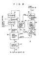
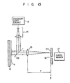
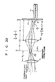
- Fig. 4 shows a schematic diagram of the embodiment of the invention.
- An object 11 to be inspected is supported in an X-Y stage 12.
- the X-Y stage 12 will be described hereinafter in detail with reference to Fig. 15.
- the object 11 which is inspected in accordance with the invention is a plate formed with a number of regularly arrayed openings or apertures as will be described in connection with Fig. 5 and following figures.
- a coherent light source 13 which may, for instance, be a helium-neon laser, produces a coherent light beam, which is enlarged by a collimator lens system 14 to an appropriate light spot diameter, for instance 8 mm.
- the enlarged parallel coherent light beam irradiates a given region of the object 11.
- the lens 15 has a Fourier transform function, and a Fourier transform conversion pattern image of the object 11 is formed on a focal plane FP which is located at a position which is distant from the lens 15 by the focal distance f thereof.
- An opening or pinhole 16 is provided on the focal plane FP, and of the aforementioned Fourier transform conversion pattern image only the diffracted light of the order n passes through the pinhole 16.
- the order n diffracted light passing through the pinhole 16 is incident on a photosensor 17, for instance a photomultiplier, and converted thereby into an electric signal In (specific datum), which is converted by an A/D converter 18 into a digital signal I D which is in turn coupled to a data processor 19.
- the result of data processing in the data processor 19 is displayed on a display device 20 which comprises, for instance, a CRT monitor.
- Designated at 21 is a stage controller for driving the X-Y stage 12.
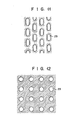
- Fig. 5 shows an example of an object inspected.
- This object is a color television picture tube shadow mask comprising a base plate formed with a number of rectangular openings 23.
- the size of the openings 23 is a H in X-axis direction and a v in Y-axis direction. These openings are regularly arranged at a pitch P H in X-axis direction and a pitch P v in the Y-axis direction.
- the object 11 is supported in the manner as shown in Fig. 4, with the X-axis direction coincident with the vertical direction of the paper of the figure and the Y-axis direction coincident with a direction perpendicular to the paper thereof, and the pinhole 16 is located in the focal plane FP at which the order n diffracted light on the spatial frequency axis (t axis) in the X-axis direction is focused.
- the electric signal In produced from the photoelectric converter 17 is given as
- Figs. 6 and 7 shows the relation between electric signal I n and variation ⁇ a H .
- ⁇ 1 ⁇ m variation of a H can be detected as +12% changes of the electric signal.
- the order number n can be appropriately selected by taking the measurement conditions, characteristic curve of the electric signal, detection sensitivity, signal-to- noise ratio, etc. into considerations.
- about 120 apertures can be simultaneously illuminated by a parallel light beam of 8 mm in diameter.
- the pinhole 16 in Fig. 4 may be located such that it permits extraction of the order n diffracted light in the ⁇ -axis perpendicular to the (-axis (i.e., in a direction perpendicular to the paper of the figure).
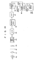
- Fig. 8 shows specific details of the data processor 19 shown in Fig. 4.
- An X-counter 31 and a Y-counter 32 count output pulses from a clock & timing pulse generator 30, and their outputs, produced as a result of counting, indicate the region of the object 11 that is illuminated by the parallel light beam.
- a code converter (ROM) 33 in which the digital datum corresponding to the characteristic curve shown in Fig. 6, for instance, is memorized.
- a data memory (RAM) 34 stores the measured or calculated average fundamental pattern size in each region.
- the X-counter 31 receives a pulse 00 supplied from the clock & timing pulse generator 30, it adds "1" as increment to its count.
- the count result data of the X- and Y-counters 31 and 32 are supplied to the stage control device 21.
- the stage control device 21 moves the X-Y stage 12 in the X- and/or Y-directions according to the count result data inputted.
- a Fourier transform pattern image of the region of the object 11 irradiated by the parallel light beam is formed through the lens 15, and its order 12 diffracted light is extracted through the pinhole 16.
- the photosensor 17 thus produces an electric signal I 12 corresponding to the intensity of the extracted order 12 diffracted light.
- the electric signal I 12 is converted by the A/D converter 18 into the digital data I D .
- This datum I D is loaded in a register 35 under the control of a pulse ⁇ 1 produced from the clock & timing pulse generator 30.
- the datum I D in the register 35 is supplied as an address designation signal to the ROM 33, whereby datum I D2 representing the average variation value ⁇ a H corresponding to the data I D is read out from the ROM 33.
- This datum I D2 is loaded in a register 36 under the control of a pulse ⁇ 2 produced from the clock & timing pulse generator 30.
- the clock & timing pulse generator 30 subsequently produces a pulse ⁇ 3
- the datum l D2 representing ⁇ a H loaded in the register 36, is written in the data memory 34 in specific address thereof designated by the contents CX and CY of the X-and Y-counters 31 and 32.
- the clock & timing signal generator 30 repeatedly produces the successive pulses 00 to ⁇ 3, the scanning or measuring of the entire area of the object 11 is obtained, and the average variation values for individual regions are successively stored in the data memory 34.
- the content DD of the data memory 34 is taken out through a display interface 37 for display on the display device 20.
- Fig. 9 shows an example of the display on the display device 20.
- the ordinate is taken for the average variation ⁇ a H and graduated in ⁇ m
- the abscissa is taken for the shift extent of the X-Y stage 12 in the X-direction and graduated in 10 mm.
- the instant embodiment is constructed such that it permits observation of the object pattern size variations in the X-axis direction
- it is also possible to obtain a two-dimensional display of fluctuations of the fundamental pattern distribution over the entire inspection object by setting up one-to-one correspondence between the points on a CRT display, for instance, and the points on each region of the object 11 and showing the average variations ⁇ a H for the individual regions with corresponding colors.
- Such a color display can be realized by modulating a color television color decoder with a signal corresponding to ⁇ a H , and this will be described hereinafter in detail.
- the Fourier transform function of a lens for inspecting all the pattern information contained in the coherent light beam transmitted through an object inspected.
- the Fourier transform has such a nature as to permit instant measurement of the average size of all fundamental pattern information contained in the transmitted beam.
- the speed of measurement obtainable is by far higher than the case of a prior art high precision measuring instrument such as a computer image processing system where the individual patterns are measured one after another for calculating the average pattern size.
- about 120 fundamental patterns contained in a 8-mm diameter laser beam can be instantly measured with a resolution of 0.1 ⁇ m.
- the precision obtainable according to the invention is by far superior to the prior art light transmittance measuring method, which is a high speed measuring method.
- the variation of the light transmittance that is obtainable with a +1 ⁇ m variation of the a H of the object inspected with the above embodiment is only about ⁇ 0.57%.
- the order 12 diffracted light intensity (I 12 ) is varied by as much as 12% with the ⁇ 1 ⁇ m as in the above embodiment. This means that according to the invention it is possible to obtain as high a sensitivity as about 20 times that in the case of the prior art light transmittance method.
- the apparatus according to the invention accurate measurement can be obtained even where the object inspected is subject to rotation by several degrees. More particularly, the pattern that is formed on the focal plane of the Fourier transform lens has an arrangement of bright spots widely spaced apart from one another. Accordingly, by forming the pinhole 16 such that it is elongate in the direction of rotation of the object, as shown in Figs.
- the diffracted light i.e., a bright spot
- the adjacent order i.e., orders (n-1)th and (n+ 1)th with respect to the order n
- correct measurement can be obtained even if the object 11 inspected is subject to rotation within, for instance, about 15° in case with the order 12 diffracted light for detection and about ⁇ 7° in case with the order 8 diffracted light.
- the measurement is determined by the a H /P H as is seen from formula (2).
- tilting of the inspected object with respect to the optical axis does not affect precision of measurement because this does not result in a change of a H /P H .
- Equation (3) defines the sensitivity S n (a H ) of the apparatus with respect to a H vs. I n .
- S n is a function of n expressed as It will be seen that n can be appropriately determined to provide a high sensitivity when a H/ P H is given by equation (4).
- the order n to be extracted should be determined with measuring condition, such as a measuring range.
- a slope sign change point (minimal or maximal level point) in the envelope pattern of the Fourier transform pattern image which bears the information about the individual fundamental patterns may be found out, and diffracted light of order n in the neighborhood of that point with much intensity (i.e., amplitude) variation may be selected for measurement.
- intensity i.e., amplitude
- the object for inspection has had openings or apertures formed in a substrate typically such as a shadow mask for television picture tube screen
- the invention is also applicable to the inspection of objects without any aperture such as a glass plate provided with fundamental patterns of an opaque material or a material having a different light transmittance.
- a light reflecting object such as metal object which is provided with fundamental patterns
- an arrangement as shown in Fig. 13 may be employed for measurement.
- a Fourier transform pattern image is formed from light reflected by an object 11. More particularly, in Fig. 13, parallel light transmitted through a half mirror 22 is incident on the object 11, and light reflected thereby is coupled through the half mirror 22 to a lens 15, which has the Fourier transform function.
- the other part of the construction is the same as in the apparatus of Fig. 4, so its description is omitted.
- a light screening tube and a color filter in front of the pinhole 16 in order to eliminate undesired external noise light being irrelevant to the measurement.
- a microcomputer may be used for the data processor 19. In this case, it is possible to provide not the relative value (i.e., variation) but the absolute value of the fundamental pattern average size by using an one-to-one correspondence table between the photosensor output and output data.
- Fig. 14 shows a different embodiment of the invention.
- the Fourier transform pattern image is electrically formed.
- light from an incandescent lamp 40 illuminates an object 42 to be inspected through a lens 41.
- the light image of a given region of the object 42 is focused through a lens 43 on a target plane of an image pick-up device 44, for instance a vidicon@,
- the image pick-up device 44 converts the incident light image into an electric signal, which is converted through an A/D converter 45 into a digital signal to be stored in a read/write memory 46.
- the image data output from the memory 46 is coupled to a fast Fourier transform unit 47, the output of which is coupled to and stored in a read/write memory 48.
- the memory 48 digital data of the two-dimensional Fourier transform pattern image of a given region is stored.
- the Fourier transform unit 47 Model AP-400, by Analogic Inc., U.S.A., for instance, may be used.
- an address corresponding to a diffracted light component of a suitable order is preset, and the content of the memory 48 for this address is selectively fetched out for arithmetic processing in the microcomputer 49.
- the average size of a plurality of fundamental patterns contained in the given region of the object 42 is obtained, and this result is displayed on a display device 50.
- This embodiment is suitable for the inspection or measurement of an object, in which fundamental patterns are formed in, e.g. an optically non-uniform glass plate.
- the Fourier transform pattern image being obtained also contains information relating to the thickness irregularities, that is, a Fourier transform pattern image concerning the thickness irregularities is superimposed upon the Fourier transform pattern image concerning the fundamental pattern size.
- Fig. 15 shows a specific example of the X-Y stage 12 shown in Fig. 4 or 13.
- the count output CY produced from the Y-counter 32 in Fig. 8 is coupled through a shift direction change switch 60Y to a conventional Y-axis pulse motor driver 62Y.
- the count output CX produced from the X-counter 31 is coupled through a similar switch 60X to an X-axis pulse motor driver 62X.
- a drive output DY from the driver 62Y is coupled to a Y-axis pulse motor 64Y for shifting the stage 12 in the Y-axis direction.
- a drive output DX from the driver 62X is coupled to an X-axis pulse motor 64X.
- the motors 64Y and 64X are rotated, for instance in the clockwise direction, according to the data CY and CX coupled to the respective drivers 62Y and 62X.
- the motor 64X shifts the stage 12 in the X-axis direction by a distance corresponding to the count value of the X-counter 31 or data CX. Every time the shift by the whole stroke in the X-axis direction is made, the output DY is incremented, and the stage 12 is shifted a predetermined amount in the Y-axis direction in accordance with the increment of the output DY.
- Fig. 16 shows a specific example of the clock & timing pulse generator 30, and Fig. 17 is a timing chart illustrating the operation sequence of the generator 30.
- An astable multivibrator (AMV) 30 1 produces a clock pulse signal 00 as shown in A in Fig. 17.
- the pulse signal ⁇ 0 constitutes the count input to the X-counter 31, and it is also coupled to a first one-shot 30 2 .
- the one-shot 30 2 is triggered by the trailing edge of the pulse ⁇ 0, and it produces a first load pulse signal ⁇ 1 as shown in D in Fig. 17.
- the counter 31 is defined as a modulo one counter (In this case the counter 31 may be omitted.).
- the loading of the datum I D in the register 35 is effected under the control of the pulse signal ⁇ 1.
- the pulse signal ⁇ 1 is also coupled to a second one-shot 30 3 .
- the second one-shot 30 3 is triggered by the trailing edge of the pulse ⁇ 1, and it produces a second load pulse signal ⁇ 2 as shown in G in Fig. 17.
- the loading of the datum I D2 from the ROM 33 to the register 36 is effected under the control of the pulse signal ⁇ 2.
- the pulse signal ⁇ 2 is also coupled to a third one-shot 30 4 ,
- the one-shot 30 4 is triggered by the trailing edge of the pulse ⁇ 2, and it produces a third load pulse signal ⁇ 3 as shown in H in Fig. 17.
- the loading of the datum I D2 form the register 36 to the RAM 34 is effected under the control of the pulse signal ⁇ 3.
- the address of the RAM 34 for storing the datum I D2 is determined by the count outputs CX and CY. If the Y-counter 32 is a modulo n counter, one output pulse CY is produced every time n pulses ⁇ 0 are produced. For example, if the Y-counter 32 is a decimal counter and has produced 128 pulses ⁇ 0 from the outset, the datum CY represents "12", and the datum CX represents "8". In this case, the datum I D2 is stored in, e.g. the address No. 128 of the RAM 34.
- Fig. 18 shows the internal construction of the microcomputer 49 shown in Fig. 14, and Fig. 19 is a flow chart illustrating the operation of the microcomputer 49.
- a main memory (ROM/RAM) 49 2 holds a data table of the In versus ⁇ a H relation as shown in, for instance, Fig. 6.
- a CPU 49 3 designates the specific address of the RAM 48 where a signal (specific datum) 1 12 is stored (step 10 of Fig. 19). Then, the contents in the designated address of the RAM 48 are loaded to a register 49, (step 12).
- the CPU 49 3 searches the data table in the memory 49 2 for variation data corresponding to the contents of the datum I 12 loaded in the register 49, and transfers variation data thus found out from the memory 49 2 to the register 49, (step 14).
- the contents thus loaded in the register 49 1 i.e., the variation data
- the device 50 makes a two-dimensional display as shown in Fig. 9.
- Figs. 20A and 20B show the case of displaying the inspection patterns as two-dimensional color display.
- the intensity of, for instance, the order 12 diffracted light component is classified into three regions by two threshold levels L i and L 2 .
- the levels L, and L 2 respectively correspond to the upper and lower limits of the nominal average pattern size.
- the region where the intensity level is above L 1 , i.e., where the pattern size is greater than the nominal size, is displayed in red, for instance.
- the region of intensities between L, and L 2 where the pattern size is the nominal size is displayed in green, for instance, and the region of intensities less than L 2 , i.e., of the pattern size less than the nominal size, is displayed in blue, for instance.
- Fig. 21 shows an example of the system for the X-Y color display.
- the display data DD produced from the data processor 19 is coupled to the level sensors 70, 72 and 74.
- the sensor 70 is a high level comparator in which L 1 is set as its reference level.
- the sensor 74 is a low level comprator in which L 2 is set as its reference level.
- the sensor 72 is a level slicer with L 1 and L 2 as its reference levels.
- the sensors 70 to 74 may be constructed with a conventional operational amplifier.
- a red modulation signal is supplied from the sensor 70 to a color decoder 76.
- L,>DD>L 2 a green modulation signal is supplied from the sensor 72 to the decoder 76.
- DD ⁇ L 2 a blue modulation signal is supplied from the sensor 74 to the decoder 76.
- the decoder 76 may be constructed with, for instance, a conventional NTSC type color decoding matrix circuit.
- the decoder 76 color decodes its input and produces a color signal CS coupled to a conventional color CRT display device 78. With the color signal input to it, the device 78 makes the X-Y color display as shown in Fig. 20B.
- Fig. 22 shows an arrangement which is effective for improving the resolution of detection of the diffracted light by the pinhole 16.
- the lens 15 forms a Fourier transform pattern image where the distance between adjacent diffracted light spots is ⁇ i on an imaginary focal plane FP. This image is focused by an enlarging lens 15A as an enlarged image on the real focal plane FP.
- the distance ⁇ between adjacent diffracted light spots is expressed as where a denotes the distance between the plane FP and the lens 15A, b the distance between the plane FP and the lens 15A, k a proportional constant, and A a wavelength of the coherent light.
- Equation (5) indicates that the resolution of the apparatus can be improved by increasing the ratio b/a, increasing the wavelength A and/or the distance f i . Particularly, a great effect can be obtained by increasing the ratio b/a.
- the enlarging lens 15A is provided for obtaining this effect.
- Fig. 14 can be replaced with an image processing module such as Model 203 by Deft Laboratories Inc., U.S.A.
Landscapes
- Physics & Mathematics (AREA)
- General Physics & Mathematics (AREA)
- Length Measuring Devices By Optical Means (AREA)
- Image Analysis (AREA)
- Investigating Materials By The Use Of Optical Means Adapted For Particular Applications (AREA)
Description
- This invention relates to an apparatus for inspecting an object by light and particularly to a pattern inspecting apparatus for measuring the average size of fundamental patterns substantially regularly arranged in a body or object to be inspected.
- Document US-A-3 954 337 discloses an apparatus for determining the average size of apertures in an apertured member. This apparatus includes a detector which is positioned to receive two adjacent light fringes on two photocells, respectively. These fringes 106a and 106b correspond to signals Vz and Vx' respectively. The average aperture width b is obtained from the relation.

- Systems for measuring the average size fundamental patterns as shown in Figs. 1 and 2 are previously known. The system shown in Fig. 1 is provided by Recognition Systems Inc., U.S.A., and called MAME system. In this system, a body 2 having an opening or aperture is illuminated by a laser or coherent light beam through a
Fourier transform lens 1, and the Fourier spectrum of the body, obtained by illumination thereof through the lens, is detected by a photodiode array 3. The output of the diode array 3 is coupled through an A/D converter (interface) 4 to amicrocomputer 5. In themicrocomputer 5, the input datum which is a Fourier transform pattern image datum is processed to obtain its autocorrelation distribution. From this autocorrelation distribution the opening or aperture size of the body 2 can be determined with high precision. - The system shown in Fig. 2 is for precisely measuring the diameter of a circular opening or aperture. In this system, an inspection pattern 6, obtained by laser beam irradiation, is coupled through a Fourier transform lens 7 to a
filter 8 disposed on the Fourier transform conversion plane, and the filter output is coupled through another Fourier transform lens 9 for photoelectric measurement on anoutput plane 10 to determine the aperture diameter (A. L. Flam- holz et al, IBM, J. Res. Develop. 1973, p. 509). - With the above measuring systems the size of a single aperture (or fundamental pattern) can be measured with high precision. However, if it is desired to obtain the average size of a number of fundamental patterns formed in a body to be inspected, considerable time is required for the measurement, because the sizes of the individual fundamental patterns have to be measured one after another before calculation of the average value.
- As a prior art method for measuring the average size of a number of openings or apertures provided on a body for inspection, it has been known to measure light transmittance for obtaining the average aperture size through calculation. However, although this method is simple, precision of measurement is inferior.
- The invention is intended in the light of the above, and its object is to provide an apparatus for inspecting average size of fundamental patterns at high speed and with high precision.
- To achieve the above object of the invention, there is provided an apparatus for inspecting an object by light, the object having a pattern of regularly arranged units or fundamental patterns, the apparatus comprising Fourier transform means for forming a Fourier transform pattern of the object, and processor means for determining the size of the fundamental patterns contained in the object from the Fourier transform pattern, said Fourier transform means including a Fourier transformer for providing output data corresponding to a Fourier transform pattern image of a given region of the object containing the regularly arrayed fundamental patterns, according to the invention said apparatus for inspecting an object includes an extractor responsive to the output data of said Fourier transformer for extracting a single specific datum representing a spatial frequency component of the order n from the output data, the magnitude of the order n component changing with variation of the size of fundamental patterns said processor means includes first means associated with said extractor for determining the average size of fundamental patterns on the given region corresponding to the single specific datum; and the order n spatial frequency component is so selected that the rate of change or the differential coefficient of the magnitude of the order n component with respect to the variation of the size of said fundamental patterns is substantially a maximum.
- Thus, according to the invention a single spatial frequency component is used for detecting the envelope pattern change and for determining the average size of the fundamental patterns.
- The invention is predicated on the fact that with a Fourier transform pattern image of an object having regularly arranged fundamental patterns the light intensity distribution of the spatial frequency components or diffracted light components (which is hereinafter referred to as an envelope pattern) changes with the size of the fundamental patterns.
- This will now be briefly discussed with reference to Figs. 3A, 3B and 3C. Fig. 3A shows the Fourier spectrum of an object having regularly arrayed fundamental patterns. In the figure, the ordinate is taken for the light intensity, and the abscissa is taken for the spatial frequency (i.e., diffraction order). The peaks of the light intensity are referred to as diffraction components of order n (n being 0, 1, 2,...), and the envelope pattern for the individual peaks is designated as 100. Similar to Fig. 3A, Figs. 3B and 3C also show envelope patterns of objects having regularly arrayed fundamental patterns. More particularly, Fig. 3B shows a Fourier spectrum in case where the fundamental patterns are slightly greater in size compared to the case of Fig. 3A, and Fig. 3C shows a Fourier spectrum in case where the fundamental pattern size is slightly less. In Figs. 3B and 3C, the respective envelope patterns are designated as 101 and 102. In the envelope pattern 101 a slope sign change point (minimum level point) A2 is closer to the
origin 0 than the corresponding slope sign change point A1 in the envelope pattern 101. (This is referred to as reduction). In the envelope pattern 102 a slope sign change point A3 is further apart from theorigin 0 than the point A1 in the envelope pattern 100. (This is referred to as enlargement.) It will be seen that since the envelope pattern changes depending upon the fundamental pattern size, light intensity information which changes even with very slight changes of the fundamental pattern size can be obtained from the measurement of the light intensity of diffraction component of a specific order in the neighborhood of the slope sign change point (i.e., extreme level point). For example, in Figs. 3A to 3C, the intensity of aspectral component 200 is reduced with an enlargement of the fundamental pattern size and increased with a reduction of the fundamental pattern size. As for an anotherspectral component 201, the light intensity is increased with increase of the fundamental pattern size and reduced with decrease of the fundamental pattern size. - Thus, even slight changes of the fundamental patterns can be detected with high precision through the measurement of the higher order spectrum light intensity. In this case, even by expanding the measurement region for simultaneously obtaining Fourier transform data for a number of fundamental patterns on the inspected object, the obtained envelope pattern has a Fourier spectrum similar to that of the envelope pattern in case of a single fundamental pattern. Thus, it is possible to obtain instant measurement of the average size of all the fundamental patterns contained in the measurement region.
- This invention can be more fully understood from the following detailed description when taken in conjunction with the accompanying drawings, in which:
- Figs. 1 and 2 show prior art apparatuses for measuring or inspecting pattern sizes;
- Figs. 3A, 3B and 3C are graphs explaining the nature of the present invention;
- Fig. 4 is a schematic diagram representing an embodiment of the invention;
- Fig. 5 shows example patterns located in a given region of a body to be inspected;
- Figs. 6 and 7 are graphs illustrating the relation between intensity (In) of the specific diffracted light component and variation (DaH) of the pattern size;
- Fig. 8 is a block diagram illustrating specific details of a
data processor 19 shown in Fig. 4; - Fig. 9 shows an example of displayed figure illustrating AaH vs. X;
- Figs. 10A, 10B and 10C show modifications of
pinhole 16 provided on the focal plane FP; - Figs. 11 and 12 show modifications of patterns shown in Fig. 5;
- Fig. 13 shows a modification of Fig. 4 apparatus;
- Fig. 14 is a schematic diagram representing another embodiment of the invention;
- Fig. 15 shows a view of X-Y stage used in the embodiments of Figs. 4 and 13;
- Fig. 16 is a block diagram illustrating specific details of a
pulse generator 30 shown in Fig. 8; - Fig. 17 is a timing chart illustrating the operation sequence of the
pulse generator 30; - Fig. 18 illustrates details of a
microcomputer 49 shown in Fig. 14; - Fig. 19 is a flow chart explaining the operation of
microcomputer 49 of Fig. 14; - Figs. 20A and 20B illustrate an example of X-Y color display indicating the variation (DaH) of patterns;
- Fig. 21 is a block diagram of a configuration for displaying variation of patterns by means of X-Y color display;
- Fig. 22 shows a partial modification of the apparatus of Fig. 4;
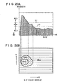
- Fig. 23A shows another example pattern to be inspected in accordance with the present invention, where apertures are located on a 3- dimensionally formed surface; and
- Fig. 23B shows a cross-sectional view taken along lines A-A' of Fig. 23A.
- Before proceeding with the description of the embodiments of the invention, it will expressly be understood that like reference symbols are used to designate like portions throughout the drawings for simplicity of illustration and that the components designated by like reference symbols may easily be replaced with each other or one another with minor change thereof by a skilled person in the art. An embodiment of the pattern inspection apparatus according to the invention will be described.
- Fig. 4 shows a schematic diagram of the embodiment of the invention. An object 11 to be inspected is supported in an
X-Y stage 12. (TheX-Y stage 12 will be described hereinafter in detail with reference to Fig. 15.) The object 11 which is inspected in accordance with the invention is a plate formed with a number of regularly arrayed openings or apertures as will be described in connection with Fig. 5 and following figures. A coherentlight source 13 which may, for instance, be a helium-neon laser, produces a coherent light beam, which is enlarged by acollimator lens system 14 to an appropriate light spot diameter, forinstance 8 mm. The enlarged parallel coherent light beam irradiates a given region of the object 11. Light transmitted through the object 11 is incident on alens 15. Thelens 15 has a Fourier transform function, and a Fourier transform conversion pattern image of the object 11 is formed on a focal plane FP which is located at a position which is distant from thelens 15 by the focal distance f thereof. An opening orpinhole 16 is provided on the focal plane FP, and of the aforementioned Fourier transform conversion pattern image only the diffracted light of the order n passes through thepinhole 16. The order n diffracted light passing through thepinhole 16 is incident on aphotosensor 17, for instance a photomultiplier, and converted thereby into an electric signal In (specific datum), which is converted by an A/D converter 18 into a digital signal ID which is in turn coupled to adata processor 19. The result of data processing in thedata processor 19 is displayed on adisplay device 20 which comprises, for instance, a CRT monitor. Designated at 21 is a stage controller for driving theX-Y stage 12. - Fig. 5 shows an example of an object inspected. This object is a color television picture tube shadow mask comprising a base plate formed with a number of
rectangular openings 23. The size of theopenings 23 is aH in X-axis direction and av in Y-axis direction. These openings are regularly arranged at a pitch PH in X-axis direction and a pitch Pv in the Y-axis direction. - The Fourier transform pattern for such inspection object is given as
- (sinc pattern)x(Fourier pattern of aperture arrangement) (1)
- Note:

- Now, the case of measuring the average value of the X-axis dimension a of the apertures in the object will be described (the case with the Y-axis dimension av being the same as the case with the X-axis dimension and thus not described).
- The object 11 is supported in the manner as shown in Fig. 4, with the X-axis direction coincident with the vertical direction of the paper of the figure and the Y-axis direction coincident with a direction perpendicular to the paper thereof, and the
pinhole 16 is located in the focal plane FP at which the order n diffracted light on the spatial frequency axis (t axis) in the X-axis direction is focused. In this arrangement, when there is a variation ΔaH in the size aH, the electric signal In produced from thephotoelectric converter 17 is given as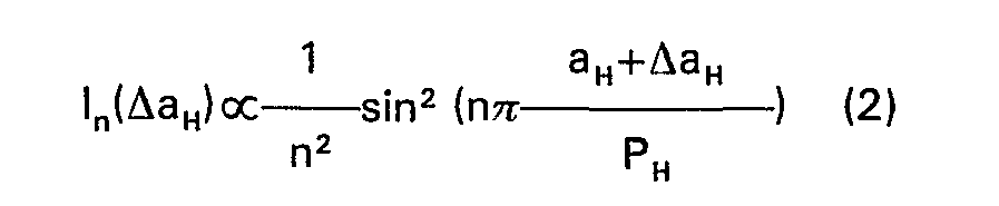
- Thus, measurement of the variation ΔaH through amplification is possible by appropriately selecting the number n and also appropriately settling the argument value of sin2, i.e., selecting an appropriate working point for the measurement.
- Figs. 6 and 7 shows the relation between electric signal In and variation ΔaH. The electric signal is unity for the object (Fig. 5) where aH=170 µm and PH=650 µm.
- Fig. 6 shows the electric signal I12 in case with n=12, i.e., in case where the
order 12 diffracted light is extracted through thepinhole 16. In this case ±1 µm variation of aH can be detected as +12% changes of the electric signal. - Fig. 7 shows the electric signal I8 in case with n=8, i.e., in case where the
order 8 diffracted light is extracted through thepinhole 16. In the actual measurement, the order number n can be appropriately selected by taking the measurement conditions, characteristic curve of the electric signal, detection sensitivity, signal-to- noise ratio, etc. into considerations. With the inspection object as mentioned above, about 120 apertures can be simultaneously illuminated by a parallel light beam of 8 mm in diameter. - For obtaining the average value of the aperture size av of the object in the Y-axis direction shown in Fig. 5, the
pinhole 16 in Fig. 4 may be located such that it permits extraction of the order n diffracted light in the η-axis perpendicular to the (-axis (i.e., in a direction perpendicular to the paper of the figure). - Fig. 8 shows specific details of the
data processor 19 shown in Fig. 4. An X-counter 31 and a Y-counter 32 count output pulses from a clock &timing pulse generator 30, and their outputs, produced as a result of counting, indicate the region of the object 11 that is illuminated by the parallel light beam. A code converter (ROM) 33 in which the digital datum corresponding to the characteristic curve shown in Fig. 6, for instance, is memorized. A data memory (RAM) 34 stores the measured or calculated average fundamental pattern size in each region. When the X-counter 31 receives apulse 00 supplied from the clock &timing pulse generator 30, it adds "1" as increment to its count. The count result data of the X- and Y-counters stage control device 21. Thestage control device 21 moves theX-Y stage 12 in the X- and/or Y-directions according to the count result data inputted. At this time, a Fourier transform pattern image of the region of the object 11 irradiated by the parallel light beam is formed through thelens 15, and itsorder 12 diffracted light is extracted through thepinhole 16. The photosensor 17 thus produces an electric signal I12 corresponding to the intensity of the extractedorder 12 diffracted light. The electric signal I12 is converted by the A/D converter 18 into the digital data ID. This datum ID is loaded in aregister 35 under the control of a pulse Ø1 produced from the clock &timing pulse generator 30. The datum ID in theregister 35 is supplied as an address designation signal to theROM 33, whereby datum ID2 representing the average variation value ΔaH corresponding to the data ID is read out from theROM 33. This datum ID2 is loaded in aregister 36 under the control of a pulse φ2 produced from the clock &timing pulse generator 30. When the clock &timing pulse generator 30 subsequently produces a pulse Ø3, the datum lD2 representing ΔaH, loaded in theregister 36, is written in thedata memory 34 in specific address thereof designated by the contents CX and CY of the X-and Y-counters - As the clock &
timing signal generator 30 repeatedly produces thesuccessive pulses 00 to φ3, the scanning or measuring of the entire area of the object 11 is obtained, and the average variation values for individual regions are successively stored in thedata memory 34. The content DD of thedata memory 34 is taken out through adisplay interface 37 for display on thedisplay device 20. - Fig. 9 shows an example of the display on the
display device 20. In the Figure, the ordinate is taken for the average variation ΔaH and graduated in µm, and the abscissa is taken for the shift extent of theX-Y stage 12 in the X-direction and graduated in 10 mm. While the instant embodiment is constructed such that it permits observation of the object pattern size variations in the X-axis direction, it is also possible to obtain a two-dimensional display of fluctuations of the fundamental pattern distribution over the entire inspection object by setting up one-to-one correspondence between the points on a CRT display, for instance, and the points on each region of the object 11 and showing the average variations ΔaH for the individual regions with corresponding colors. Such a color display can be realized by modulating a color television color decoder with a signal corresponding to ΔaH, and this will be described hereinafter in detail. - Now, the effects of the invention will be discussed.
- In one embodiment of the invention, use is made of the Fourier transform function of a lens for inspecting all the pattern information contained in the coherent light beam transmitted through an object inspected. The Fourier transform has such a nature as to permit instant measurement of the average size of all fundamental pattern information contained in the transmitted beam. Thus, according to the invention the speed of measurement obtainable is by far higher than the case of a prior art high precision measuring instrument such as a computer image processing system where the individual patterns are measured one after another for calculating the average pattern size. With the above embodiment of the present invention, about 120 fundamental patterns contained in a 8-mm diameter laser beam can be instantly measured with a resolution of 0.1 µm. If the same resolution is to be provided for data processing with a computer processing system, as large a bit number as about 5×109 bits is required for the aforementioned 8-mm diameter input data. In this case, some 5 seconds is required for the measurement with a processing rate of 1 nsec. per bit.
- I In the second place, the precision obtainable according to the invention is by far superior to the prior art light transmittance measuring method, which is a high speed measuring method. With the usual case of light transmittance measurement, the variation of the light transmittance that is obtainable with a +1 µm variation of the aH of the object inspected with the above embodiment is only about ±0.57%. In contrast, according to the invention the
order 12 diffracted light intensity (I12) is varied by as much as 12% with the ±1 µm as in the above embodiment. This means that according to the invention it is possible to obtain as high a sensitivity as about 20 times that in the case of the prior art light transmittance method. - Further, with the apparatus according to the invention, accurate measurement can be obtained even where the object inspected is subject to rotation by several degrees. More particularly, the pattern that is formed on the focal plane of the Fourier transform lens has an arrangement of bright spots widely spaced apart from one another. Accordingly, by forming the
pinhole 16 such that it is elongate in the direction of rotation of the object, as shown in Figs. 10A to 10C, to such an extent that the diffracted light (i.e., a bright spot) can be detected without extraction of the diffracted light of the adjacent order (i.e., orders (n-1)th and (n+ 1)th with respect to the order n), correct measurement can be obtained even if the object 11 inspected is subject to rotation within, for instance, about 15° in case with theorder 12 diffracted light for detection and about ±7° in case with theorder 8 diffracted light. - In addition, with the apparatus according to the invention the measurement is determined by the aH/PH as is seen from formula (2). Thus, tilting of the inspected object with respect to the optical axis does not affect precision of measurement because this does not result in a change of aH/PH. This further means that correct pattern size measurement can be obtained even where the object 11 is three-dimensionally deformed; that is, accurate pattern size measurement can be obtained in case of an object 11 as shown in Figs. 23A and 23B, which is prepared from a flat plate with a press.
- Further, it will be apparent from the principles of measurement that even if the inspection object is shifted in the X- and Y-directions instant measurement of the region irradiated by a beam can be obtained. This means that no positioning adjustment of the object is needed, and measurement can be made while moving the object.
- Further, by using a parallel light beam for illumination, accurate measurement can be obtained even when the object is displaced in the direction of the beam axis, that is, no fucus- ing is needed. Thus, with an object having a shape as shown in Figs. 23A and 23B, no particular focusing mechanism is needed for the measurement.
- Rearranging formula (2) we obtain


- As has been shown, according to the invention it is possible to provide a practical measuring apparatus, with which the precision requirement is less strict in spite of the fact that high speed and high precision measurement is possible.
- Now, some modifications of the above embodiment of the invention will be described. While in the above embodiment the object for inspection has had regularly arrayed rectangular apertures as shown in Fig. 5, this is by no means limitative, and an object having fundamental patterns of any shape, such as oval apertures as shown in Fig. 11 or circular apertures as shown in Fig. 12, can be inspected insofar as the patterns are substantially regularly arrayed. With the inspection objects shown in Figs. 11 and 12, however, formulas (1) to (4) do not hold. Accordingly, with these objects a slope sign change point (minimal or maximal level point) in the envelope pattern of the Fourier transform pattern image which bears the information about the individual fundamental patterns may be found out, and diffracted light of order n in the neighborhood of that point with much intensity (i.e., amplitude) variation may be selected for measurement. By so doing, high sensitivity measurement can be obtained.
- In another aspect, while in the above embodiment the object for inspection has had openings or apertures formed in a substrate typically such as a shadow mask for television picture tube screen, the invention is also applicable to the inspection of objects without any aperture such as a glass plate provided with fundamental patterns of an opaque material or a material having a different light transmittance. Further, in case of a light reflecting object such as metal object which is provided with fundamental patterns, an arrangement as shown in Fig. 13 may be employed for measurement. In this arrangement, a Fourier transform pattern image is formed from light reflected by an object 11. More particularly, in Fig. 13, parallel light transmitted through a half mirror 22 is incident on the object 11, and light reflected thereby is coupled through the half mirror 22 to a
lens 15, which has the Fourier transform function. The other part of the construction is the same as in the apparatus of Fig. 4, so its description is omitted. - In the arrangement of Fig. 4, the extraction of order n diffracted light on the focal plane can be made more easy when patterns of an object are spaced apart with a large pitch by means of disposing, in the light path, a
lens 15 for enlarging the Fourier transform pattern image. - Also, it is possible to dispose a light screening tube and a color filter in front of the
pinhole 16 in order to eliminate undesired external noise light being irrelevant to the measurement. Further, a microcomputer may be used for thedata processor 19. In this case, it is possible to provide not the relative value (i.e., variation) but the absolute value of the fundamental pattern average size by using an one-to-one correspondence table between the photosensor output and output data. - Fig. 14 shows a different embodiment of the invention.
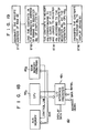
- In this embodiment, the Fourier transform pattern image is electrically formed. In the figure, light from an
incandescent lamp 40 illuminates an object 42 to be inspected through alens 41. The light image of a given region of the object 42 is focused through alens 43 on a target plane of an image pick-updevice 44, for instance a vidicon@, The image pick-updevice 44 converts the incident light image into an electric signal, which is converted through an A/D converter 45 into a digital signal to be stored in a read/write memory 46. The image data output from thememory 46 is coupled to a fastFourier transform unit 47, the output of which is coupled to and stored in a read/write memory 48. Thus, in thememory 48 digital data of the two-dimensional Fourier transform pattern image of a given region is stored. As theFourier transform unit 47, Model AP-400, by Analogic Inc., U.S.A., for instance, may be used. - In the
microcomputer 49, an address corresponding to a diffracted light component of a suitable order is preset, and the content of thememory 48 for this address is selectively fetched out for arithmetic processing in themicrocomputer 49. As a result of processing, the average size of a plurality of fundamental patterns contained in the given region of the object 42 is obtained, and this result is displayed on adisplay device 50. - This embodiment is suitable for the inspection or measurement of an object, in which fundamental patterns are formed in, e.g. an optically non-uniform glass plate. For example, in case of an inspection of a glass substrate which is not uniform in thickness, with the optical Fourier transform system as shown in Fig. 4, the Fourier transform pattern image being obtained also contains information relating to the thickness irregularities, that is, a Fourier transform pattern image concerning the thickness irregularities is superimposed upon the Fourier transform pattern image concerning the fundamental pattern size. With this embodiment, such a phenomenon can be eliminated, and it is possible to ensure high precision of measurement. Also, it is possible to obtain measurement free from the influence of any contamination of the inspected object, for instance a fingerprint stuck thereon.
- Fig. 15 shows a specific example of the
X-Y stage 12 shown in Fig. 4 or 13. Referring to the Figure, the count output CY produced from the Y-counter 32 in Fig. 8 is coupled through a shiftdirection change switch 60Y to a conventional Y-axispulse motor driver 62Y. Similarly, the count output CX produced from the X-counter 31 is coupled through asimilar switch 60X to an X-axispulse motor driver 62X. A drive output DY from thedriver 62Y is coupled to a Y-axis pulse motor 64Y for shifting thestage 12 in the Y-axis direction. Similarly, a drive output DX from thedriver 62X is coupled to anX-axis pulse motor 64X. Themotors respective drivers motor 64X shifts thestage 12 in the X-axis direction by a distance corresponding to the count value of the X-counter 31 or data CX. Every time the shift by the whole stroke in the X-axis direction is made, the output DY is incremented, and thestage 12 is shifted a predetermined amount in the Y-axis direction in accordance with the increment of the output DY. - Fig. 16 shows a specific example of the clock &
timing pulse generator 30, and Fig. 17 is a timing chart illustrating the operation sequence of thegenerator 30. An astable multivibrator (AMV) 301 produces aclock pulse signal 00 as shown in A in Fig. 17. The pulse signal φ0 constitutes the count input to the X-counter 31, and it is also coupled to a first one-shot 302. The one-shot 302 is triggered by the trailing edge of the pulse φ0, and it produces a first load pulse signal φ1 as shown in D in Fig. 17. To simplify the construction, in Fig. 17, thecounter 31 is defined as a modulo one counter (In this case thecounter 31 may be omitted.). The loading of the datum ID in theregister 35 is effected under the control of the pulse signal φ1. - The pulse signal φ1 is also coupled to a second one-
shot 303. The second one-shot 303 is triggered by the trailing edge of the pulse φ1, and it produces a second load pulse signal φ2 as shown in G in Fig. 17. The loading of the datum ID2 from theROM 33 to theregister 36 is effected under the control of the pulse signal φ2. - The pulse signal φ2 is also coupled to a third one-
shot 304, The one-shot 304 is triggered by the trailing edge of the pulse φ2, and it produces a third load pulse signal φ3 as shown in H in Fig. 17. The loading of the datum ID2 form theregister 36 to theRAM 34 is effected under the control of the pulse signal φ3. - The address of the
RAM 34 for storing the datum ID2 is determined by the count outputs CX and CY. If the Y-counter 32 is a modulo n counter, one output pulse CY is produced every time n pulses φ0 are produced. For example, if the Y-counter 32 is a decimal counter and has produced 128 pulses φ0 from the outset, the datum CY represents "12", and the datum CX represents "8". In this case, the datum ID2 is stored in, e.g. the address No. 128 of theRAM 34. - Fig. 18 shows the internal construction of the
microcomputer 49 shown in Fig. 14, and Fig. 19 is a flow chart illustrating the operation of themicrocomputer 49. Referring to Fig. 18, a main memory (ROM/RAM) 492 holds a data table of the In versus ΔaH relation as shown in, for instance, Fig. 6. When making inspection of theorder 12 diffracted light component, for instance, aCPU 493 designates the specific address of theRAM 48 where a signal (specific datum) 112 is stored (step 10 of Fig. 19). Then, the contents in the designated address of theRAM 48 are loaded to aregister 49, (step 12). In consequence, theCPU 493 searches the data table in thememory 492 for variation data corresponding to the contents of the datum I12 loaded in theregister 49, and transfers variation data thus found out from thememory 492 to theregister 49, (step 14). The contents thus loaded in the register 491 (i.e., the variation data) are then transferred as display data to the display device 50 (step 16). As a result, thedevice 50 makes a two-dimensional display as shown in Fig. 9. - Figs. 20A and 20B show the case of displaying the inspection patterns as two-dimensional color display. In this case, the intensity of, for instance, the
order 12 diffracted light component is classified into three regions by two threshold levels Li and L2. The levels L, and L2 respectively correspond to the upper and lower limits of the nominal average pattern size. The region where the intensity level is above L1, i.e., where the pattern size is greater than the nominal size, is displayed in red, for instance. The region of intensities between L, and L2 where the pattern size is the nominal size is displayed in green, for instance, and the region of intensities less than L2, i.e., of the pattern size less than the nominal size, is displayed in blue, for instance. - Fig. 21 shows an example of the system for the X-Y color display. The display data DD produced from the
data processor 19 is coupled to thelevel sensors sensor 70 is a high level comparator in which L1 is set as its reference level. Thesensor 74 is a low level comprator in which L2 is set as its reference level. Thesensor 72 is a level slicer with L1 and L2 as its reference levels. Thesensors 70 to 74 may be constructed with a conventional operational amplifier. - When the intensity In corresponds to DD>L1, a red modulation signal is supplied from the
sensor 70 to acolor decoder 76. When L,>DD>L2, a green modulation signal is supplied from thesensor 72 to thedecoder 76. When DD<L2, a blue modulation signal is supplied from thesensor 74 to thedecoder 76. Thedecoder 76 may be constructed with, for instance, a conventional NTSC type color decoding matrix circuit. Thedecoder 76 color decodes its input and produces a color signal CS coupled to a conventional colorCRT display device 78. With the color signal input to it, thedevice 78 makes the X-Y color display as shown in Fig. 20B. - Fig. 22 shows an arrangement which is effective for improving the resolution of detection of the diffracted light by the
pinhole 16. Thelens 15 forms a Fourier transform pattern image where the distance between adjacent diffracted light spots is Δζi on an imaginary focal plane FP. This image is focused by an enlarginglens 15A as an enlarged image on the real focal plane FP. The distance Δξ between adjacent diffracted light spots is expressed as
lens 15A, b the distance between the plane FP and thelens 15A, k a proportional constant, and A a wavelength of the coherent light. - Equation (5) indicates that the resolution of the apparatus can be improved by increasing the ratio b/a, increasing the wavelength A and/or the distance fi. Particularly, a great effect can be obtained by increasing the ratio b/a. The enlarging
lens 15A is provided for obtaining this effect. - Although the specific construction has been illustrated and described herein, it is not intended that the invention be limited to the elements and the construction or configuration disclosed. One skilled in the art will recognize the particular elements or sub-constructions may be used without departing from the scope and spirit of the invention. For example, the invention is applicable for use in combination with the apparatuses disclosed in Japanese Patent Applications No. 31020/79 (USSN: 130,370) and No. 143228/79 (USSN: 202,320) by the same inventors as to the instant invention.
- Furthermore, the
components 44 to 48 shown in Fig. 14 can be replaced with an image processing module such as Model 203 by Deft Laboratories Inc., U.S.A.
Claims (11)
Applications Claiming Priority (2)
| Application Number | Priority Date | Filing Date | Title |
|---|---|---|---|
| JP27321/80 | 1980-03-06 | ||
| JP2732180A JPS56124003A (en) | 1980-03-06 | 1980-03-06 | Measuring device for pattern |
Publications (2)
| Publication Number | Publication Date |
|---|---|
| EP0035720A1 EP0035720A1 (en) | 1981-09-16 |
| EP0035720B1 true EP0035720B1 (en) | 1984-08-22 |
Family
ID=12217803
Family Applications (1)
| Application Number | Title | Priority Date | Filing Date |
|---|---|---|---|
| EP81101449A Expired EP0035720B1 (en) | 1980-03-06 | 1981-02-27 | Apparatus for inspecting an object by light |
Country Status (5)
| Country | Link |
|---|---|
| US (1) | US4408883A (en) |
| EP (1) | EP0035720B1 (en) |
| JP (1) | JPS56124003A (en) |
| CA (1) | CA1152216A (en) |
| DE (1) | DE3165619D1 (en) |
Cited By (1)
| Publication number | Priority date | Publication date | Assignee | Title |
|---|---|---|---|---|
| RU2777555C2 (en) * | 2017-06-22 | 2022-08-08 | Чанчунь Мэйхэ Сайэнс Энд Текнолоджи Девелопмент Ко., Лтд | Catalyst based on acid-resistant alloy |
Families Citing this family (13)
| Publication number | Priority date | Publication date | Assignee | Title |
|---|---|---|---|---|
| US4517338A (en) * | 1983-06-20 | 1985-05-14 | Chiron Corporation | Multiple reactor system and method for polynucleotide synthesis |
| US4706018A (en) * | 1984-11-01 | 1987-11-10 | International Business Machines Corporation | Noncontact dynamic tester for integrated circuits |
| US4641256A (en) * | 1984-12-04 | 1987-02-03 | Rca Corporation | System and method for measuring energy transmission through a moving aperture pattern |
| US4786864A (en) * | 1985-03-29 | 1988-11-22 | International Business Machines Corporation | Photon assisted tunneling testing of passivated integrated circuits |
| FR2608269B1 (en) * | 1986-12-10 | 1989-04-07 | Guillaume Michel | METHOD FOR QUANTITATIVE DETERMINATION OF RELIEF PATTERNS OF VERY SMALL DIMENSIONS |
| US5293426A (en) * | 1990-05-25 | 1994-03-08 | R. R. Donnelley & Sons Company | Printing cylinder engraver calibration system and method |
| US5422958A (en) * | 1990-05-25 | 1995-06-06 | R. R. Donnelley & Sons Company | Printing cylinder engraver calibration system and method |
| JP3161085B2 (en) * | 1992-10-13 | 2001-04-25 | 松下電器産業株式会社 | Track width error inspection device |
| US5307294A (en) * | 1992-12-22 | 1994-04-26 | Aman James A | Automated end tally system |
| NL1004194C2 (en) * | 1996-10-04 | 1998-04-07 | Bmc Ind | Laser sensor for measuring characteristics of material sheet with openings. |
| CN109107581A (en) | 2017-06-22 | 2019-01-01 | 长春美禾科技发展有限公司 | A kind of acid resisting alloy catalyst |
| US11137485B2 (en) | 2019-08-06 | 2021-10-05 | Waymo Llc | Window occlusion imager near focal plane |
| CN113720266B (en) * | 2021-08-27 | 2022-10-14 | 西安电子科技大学 | Circuit board via hole copper deposition quality detection method based on optical Fourier transform |
Citations (1)
| Publication number | Priority date | Publication date | Assignee | Title |
|---|---|---|---|---|
| EP0017371A1 (en) * | 1979-03-19 | 1980-10-15 | Kabushiki Kaisha Toshiba | Apparatus for inspecting defects in a periodic pattern |
Family Cites Families (5)
| Publication number | Priority date | Publication date | Assignee | Title |
|---|---|---|---|---|
| US3441351A (en) * | 1965-05-03 | 1969-04-29 | Atomic Energy Commission | Color recording averaging light intensity meter |
| CH534342A (en) * | 1971-07-17 | 1973-02-28 | Bbc Brown Boveri & Cie | Procedure for measuring small objects |
| US3954337A (en) * | 1974-10-04 | 1976-05-04 | Rca Corporation | Method and apparatus for determining the average size of apertures in an apertured member |
| US4200396A (en) * | 1977-12-19 | 1980-04-29 | Rca Corporation | Optically testing the lateral dimensions of a pattern |
| JPS5537919A (en) * | 1978-09-11 | 1980-03-17 | Ngk Insulators Ltd | Automatic outer configuration measurement device |
-
1980
- 1980-03-06 JP JP2732180A patent/JPS56124003A/en active Pending
-
1981
- 1981-02-27 EP EP81101449A patent/EP0035720B1/en not_active Expired
- 1981-02-27 DE DE8181101449T patent/DE3165619D1/en not_active Expired
- 1981-03-04 CA CA000372294A patent/CA1152216A/en not_active Expired
- 1981-03-04 US US06/240,603 patent/US4408883A/en not_active Expired - Lifetime
Patent Citations (1)
| Publication number | Priority date | Publication date | Assignee | Title |
|---|---|---|---|---|
| EP0017371A1 (en) * | 1979-03-19 | 1980-10-15 | Kabushiki Kaisha Toshiba | Apparatus for inspecting defects in a periodic pattern |
Cited By (1)
| Publication number | Priority date | Publication date | Assignee | Title |
|---|---|---|---|---|
| RU2777555C2 (en) * | 2017-06-22 | 2022-08-08 | Чанчунь Мэйхэ Сайэнс Энд Текнолоджи Девелопмент Ко., Лтд | Catalyst based on acid-resistant alloy |
Also Published As
| Publication number | Publication date |
|---|---|
| CA1152216A (en) | 1983-08-16 |
| EP0035720A1 (en) | 1981-09-16 |
| JPS56124003A (en) | 1981-09-29 |
| DE3165619D1 (en) | 1984-09-27 |
| US4408883A (en) | 1983-10-11 |
Similar Documents
| Publication | Publication Date | Title |
|---|---|---|
| EP0028774B1 (en) | Apparatus for detecting defects in a periodic pattern | |
| EP0035720B1 (en) | Apparatus for inspecting an object by light | |
| US6172349B1 (en) | Autofocusing apparatus and method for high resolution microscope system | |
| US4147052A (en) | Hardness tester | |
| US4559603A (en) | Apparatus for inspecting a circuit pattern drawn on a photomask used in manufacturing large scale integrated circuits | |
| US5128550A (en) | Method of and an apparatus for testing large area panes for optical quality | |
| EP0197199A1 (en) | Apparatus for and a method of measuring the thickness of a film | |
| GB2051349A (en) | Automatic defecting inspection apparatus | |
| US4652765A (en) | Edge detecting device in optical measuring instrument | |
| IE41868B1 (en) | Non-contact dimentsional measurement technique | |
| US4659936A (en) | Line width measuring device and method | |
| US4652738A (en) | Edge detecting device in optical measuring instrument | |
| US6735333B1 (en) | Pattern inspection apparatus | |
| JPS6175236A (en) | Apparatus for measuring coated surface | |
| US4884890A (en) | Method for normalizing the detection signals of magnified images of fluorescing materials | |
| JPH0697203B2 (en) | Particle aggregation determination device | |
| CN107329373B (en) | A kind of overlay error measuring device and method | |
| JPH07128032A (en) | Method and apparatus for inspecting surface waviness of plate-shaped material | |
| JPH0915151A (en) | Diffusion characteristic measuring device | |
| US6332047B1 (en) | Test equipment for color printing | |
| JPS6034699B2 (en) | hardness tester | |
| JPH061177B2 (en) | Method of measuring smoothness of coated surface | |
| KR0181993B1 (en) | Apparatus and method for measuring visual size of material | |
| JP3562076B2 (en) | Spectral sensitivity measurement device | |
| JPH0726838B2 (en) | Painted surface measuring device |
Legal Events
| Date | Code | Title | Description |
|---|---|---|---|
| PUAI | Public reference made under article 153(3) epc to a published international application that has entered the european phase |
Free format text: ORIGINAL CODE: 0009012 |
|
| AK | Designated contracting states |
Designated state(s): DE FR GB NL |
|
| 17P | Request for examination filed |
Effective date: 19810227 |
|
| GRAA | (expected) grant |
Free format text: ORIGINAL CODE: 0009210 |
|
| AK | Designated contracting states |
Designated state(s): DE FR GB NL |
|
| RAP2 | Party data changed (patent owner data changed or rights of a patent transferred) |
Owner name: KABUSHIKI KAISHA TOSHIBA |
|
| REF | Corresponds to: |
Ref document number: 3165619 Country of ref document: DE Date of ref document: 19840927 |
|
| ET | Fr: translation filed | ||
| REG | Reference to a national code |
Ref country code: FR Ref legal event code: CD |
|
| PLBE | No opposition filed within time limit |
Free format text: ORIGINAL CODE: 0009261 |
|
| STAA | Information on the status of an ep patent application or granted ep patent |
Free format text: STATUS: NO OPPOSITION FILED WITHIN TIME LIMIT |
|
| 26N | No opposition filed | ||
| REG | Reference to a national code |
Ref country code: GB Ref legal event code: 746 |
|
| PGFP | Annual fee paid to national office [announced via postgrant information from national office to epo] |
Ref country code: FR Payment date: 19960125 Year of fee payment: 16 |
|
| PGFP | Annual fee paid to national office [announced via postgrant information from national office to epo] |
Ref country code: GB Payment date: 19960219 Year of fee payment: 16 |
|
| PGFP | Annual fee paid to national office [announced via postgrant information from national office to epo] |
Ref country code: DE Payment date: 19960227 Year of fee payment: 16 |
|
| PGFP | Annual fee paid to national office [announced via postgrant information from national office to epo] |
Ref country code: NL Payment date: 19960229 Year of fee payment: 16 |
|
| PG25 | Lapsed in a contracting state [announced via postgrant information from national office to epo] |
Ref country code: GB Effective date: 19970227 |
|
| PG25 | Lapsed in a contracting state [announced via postgrant information from national office to epo] |
Ref country code: NL Effective date: 19970901 |
|
| GBPC | Gb: european patent ceased through non-payment of renewal fee |
Effective date: 19970227 |
|
| PG25 | Lapsed in a contracting state [announced via postgrant information from national office to epo] |
Ref country code: FR Effective date: 19971030 |
|
| PG25 | Lapsed in a contracting state [announced via postgrant information from national office to epo] |
Ref country code: DE Effective date: 19971101 |
|
| NLV4 | Nl: lapsed or anulled due to non-payment of the annual fee |
Effective date: 19970901 |
|
| REG | Reference to a national code |
Ref country code: FR Ref legal event code: ST |