EP0033496B1 - Three-terminal semiconductor device - Google Patents
Three-terminal semiconductor device Download PDFInfo
- Publication number
- EP0033496B1 EP0033496B1 EP19810100497 EP81100497A EP0033496B1 EP 0033496 B1 EP0033496 B1 EP 0033496B1 EP 19810100497 EP19810100497 EP 19810100497 EP 81100497 A EP81100497 A EP 81100497A EP 0033496 B1 EP0033496 B1 EP 0033496B1
- Authority
- EP
- European Patent Office
- Prior art keywords
- region
- emitter
- section
- collector
- base
- Prior art date
- Legal status (The legal status is an assumption and is not a legal conclusion. Google has not performed a legal analysis and makes no representation as to the accuracy of the status listed.)
- Expired
Links
- 239000004065 semiconductor Substances 0.000 title claims description 20
- 230000004888 barrier function Effects 0.000 claims description 51
- 239000000969 carrier Substances 0.000 claims description 24
- 239000002184 metal Substances 0.000 claims description 19
- 239000000463 material Substances 0.000 claims description 10
- 229910001218 Gallium arsenide Inorganic materials 0.000 claims description 6
- 238000009826 distribution Methods 0.000 claims description 2
- 238000000926 separation method Methods 0.000 claims description 2
- 238000010586 diagram Methods 0.000 description 7
- 238000000034 method Methods 0.000 description 3
- 230000002596 correlated effect Effects 0.000 description 2
- 230000000875 corresponding effect Effects 0.000 description 2
- 238000004519 manufacturing process Methods 0.000 description 2
- 230000004048 modification Effects 0.000 description 2
- 238000012986 modification Methods 0.000 description 2
- 230000007480 spreading Effects 0.000 description 2
- 238000003892 spreading Methods 0.000 description 2
- 238000009825 accumulation Methods 0.000 description 1
- 230000003321 amplification Effects 0.000 description 1
- 230000015556 catabolic process Effects 0.000 description 1
- 230000005574 cross-species transmission Effects 0.000 description 1
- 230000007547 defect Effects 0.000 description 1
- 230000002939 deleterious effect Effects 0.000 description 1
- 230000000694 effects Effects 0.000 description 1
- 239000002784 hot electron Substances 0.000 description 1
- 239000012535 impurity Substances 0.000 description 1
- 238000002347 injection Methods 0.000 description 1
- 239000007924 injection Substances 0.000 description 1
- 238000001451 molecular beam epitaxy Methods 0.000 description 1
- 238000003199 nucleic acid amplification method Methods 0.000 description 1
- 238000005036 potential barrier Methods 0.000 description 1
- 230000008569 process Effects 0.000 description 1
- 230000004044 response Effects 0.000 description 1
- 230000001052 transient effect Effects 0.000 description 1
Images


Classifications
-
- H—ELECTRICITY
- H01—ELECTRIC ELEMENTS
- H01L—SEMICONDUCTOR DEVICES NOT COVERED BY CLASS H10
- H01L29/00—Semiconductor devices specially adapted for rectifying, amplifying, oscillating or switching and having potential barriers; Capacitors or resistors having potential barriers, e.g. a PN-junction depletion layer or carrier concentration layer; Details of semiconductor bodies or of electrodes thereof ; Multistep manufacturing processes therefor
- H01L29/66—Types of semiconductor device ; Multistep manufacturing processes therefor
- H01L29/68—Types of semiconductor device ; Multistep manufacturing processes therefor controllable by only the electric current supplied, or only the electric potential applied, to an electrode which does not carry the current to be rectified, amplified or switched
- H01L29/76—Unipolar devices, e.g. field effect transistors
- H01L29/7606—Transistor-like structures, e.g. hot electron transistor [HET]; metal base transistor [MBT]
Definitions
- the technical field of the invention is that of semiconductor devices that perform amplification with very wide bandwidth and switching in the 10- 12 second range.
- the invention as claimed concerns a semi- conductor device having emitter and collector regions, each forming separated rectifying contact with a base region, said base region having high conductivity and a separation dimension from said emitter to said collector that of the order of the length of the mean free carrier path. It is characterized by said emitter region having in a first section adjacent to an ohmic contact a source of carriers positioning the conduction band of said semiconductor material below the Fermi level in said first section, and in a second section adjacent to said base region providing a barrier of a first magnitude and having a dimension of the order of the length of the mean free path of an electron, and said collector region having a barrier to electron flow of a second magnitude greater than said first magnitude.
- a schematic structural illustration of an embodiment of the invention is provided having an emitter region 1, a base region 2 and a collector region 3, each in turn having respectively an emitter external connection 4, a base external connection 5 and a collector external connection 6.
- the emitter region 1 is made up of two sections 7 and 8.
- the first emitter section 7 serves as a large supply of carriers, is labelled N + and may be conveniently formed by heavy doping.
- the second emitter section 8 provides a low barrier to injected carrier flow into the base region 2.
- the emitter section 8 is labelled N- and may be formed by lightly doping within the section defined by the width dimension labelled d Ee .
- the base region 2 is made of high conductivity material such as metal having a width in the vicinity of the length of the mean free path of an electron so that carrier transit time and the number of collisions are minimized.
- the collector region is made up of a first section 9, labelled N, forming a barrier to carrier flow in the base.
- the collector barrier is higher than the barrier that is formed by the emitter section 8.
- the collector region 3 also has a second collector section 10 labelled N + which serves to keep the collector resistance and ohmic contact resistance low, and which may be concurrently fabricated by heavier doping.
- the N, N + and N- designations in Fig. 1 are provided to indicate relative doping with conductivity type determining impurities.
- the criteria of the collector region 3 are satisfied by the Schottky barrier type contact known in the art.
- FIG. 2 an energy level diagram dimensionally correlated with the structure of Fig. 1 is provided showing in a first portion corresponding to the section 7 of Fig. 1, a condition wherein the conduction band is below the Fermi level thereby providing a large reservoir of carriers.
- a second portion corresponding to section 8 of Fig. 1 as the emitter barrier width labelled d EB the number of available carriers is reduced such as by light doping. This has the effect that the conduction band then rises and produces barrier height labelled ⁇ E .
- the height of the barrier is controlled by the semiconductor metal interface. It should be noted, however, that for very small values of emitter barrier with the doping level of the reservoir of carriers in section 7 asserts some control.
- the adjacent high conductivity metal base 2 operates to establish the conduction band at a lower level and reduces the base spreading resistance.
- the width of the metal base is in the vicinity of the length of the mean free path of an electron to minimize transit time and number of collisions.
- the collector barrier height ⁇ c is illustrated.
- the collector barrier height (p c is higher than the emitter barrier height ⁇ E .
- the conduction band then parabolically becomes lower through the Fermi level as a result of the heavy doping of collector section 10 thereby to reduce collector resistance and minimize contact resistance.
- the metal base 2 adjacent to the section 8 which is a lightly doped thin dimensioned semiconductor section operates to provide a low barrier and an immediate potential drop to an injected carrier. The advantages of a low base spreading resistance with an injection barrier are thus simultaneously provided.
- the invention operates by providing a large source of carriers impeded by a low thin barrier in the emitter adjacent to a metal base so that having traversed the barrier, the carriers are accelerated by the potential drop toward the base and due to the thin emitter and base regions, transit time to the collector barrier is short.
- the criteria of the structure of the invention can be met in fabrication by a number of semi- conductor process techniques.
- the technique of molecular beam epitaxy is favored for its controllability.
- an output performance graph is provided illustrating the operating characteristics under the influence of bias in what is known for three-terminal devices as the common base operation.
- Operating curves labelled a, b and c are provided for three illustrative levels of emitter-base bias V EB .
- the curve a is for the condition O ⁇ V EB ⁇ c/e .
- the curve b is for the condition V EB +0.1 V.
- the curve c is for the condition V EB +0.2 V.
- the various operating curves merge into a single line labelled x, defined by the forward characteristics of the emitter barrier.
- the various operational curves merge to a single line labelled y, defined by the breakdown voltage of the reversely biased collector barrier.
- the slope of the performance curves in the region z closely parallel to the ordinate, are defined by the reverse saturation current of the collector barrier.
- the load line crosses the operating curves at two points, which when the device is used in a switching mode define the "on" or "off" conditions.
- a dotted line encompasses a range for continuous operation.
- the continuous operation range is defined by the conditions where the emitter-base bias voltage is greater than the collector barrier height divided by e.
- Fig. 5 which illustrates the input characteristics in the common emitter type of circuit operation
- the onset of a dynamic negative resistance is observed at the value of V EB equivalent to the collector barrier height divided by e.
- the device of Fig. 1 has certain features critical to its operation.
- For emitter region 1 it is required that there be a first section adjacent to the input terminal that serves as a supplier of carriers, and that there be a semi-conductor section 8 adjacent to a metal base which provides a barrier at the interface with the section 7, and that the second section 8 have a very thin dimension.
- These conditions may be met by constructing sections 7 and 8 using the material GaAs for the section 7 doped to about 5x10 18 and for the section 8 reducing the doping to about 10 15 .
- the semiconductor material chosen for the emitter section 8 should have a wide energy gap so that few thermal carriers will exist in the conduction band.
- the emitter current density will be space- charge limited for low voltages and obeys an expression known in the art as "Child's Law", as described in Equation 1.
- Equation 1 where s is the dielectric constant.
- e is the electron charge
- m * is the electron effective mass
- the transit time through the emitter region is considered to follow the expression in Equation 2 for the material GaAs.
- An example device constructed of the material may be biased under the conditions set forth in Table I.
- the traverse time (T) through the emitter as determined by Equation 2 will be 10- 13 seconds.
- the traverse time through the metal base will also be 10- 13 seconds where the base width d B is selected to be 100A
- the collector barrier is of the type known in the art as a Schottky barrier.
- the input time constant of the device of the invention using the example GaAs material is in the vicinity of 0.4x10 -13 seconds so that the speed limitation of the device will be determined by the base-collector barrier which in turn responds in the vicinity of 10- 13 seconds.
- the emitter base bias voltage will occur mostly across section 8, the thin lightly doped region.
- a variation in the structure of Fig. 1 can be provided wherein the section 8 of the emitter region is a semiconductor such as CdS which forms a non-rectifying contact with the base 2 and the emitter.
- the emitter barrier width should be made wide enough that the accumulation layers which make the semiconductor degenerate on both sides next to the interfaces with the metal will not swamp the total film thickness. This is illustrated by the fact that the conduction band potential level arcs up above the Fermi level inside d Ee .
- the dimension for the emitter barrier width should increase to about 600A.
- bias provides carriers from the metal-emitter contact over the barrier in the non-rectifying semi- conductor and the thin dimensions of both the emitter barrier region and the base permit the carriers to be accelerated directly over the collector barrier without losing any energy due to electron-electron and electron-phonon collisions.
- the lightly doped N- section and the non-rectifying semiconductor CdS section are empty of free carriers and thereby support the potential difference V EB .
- carriers spill over a small barrier at the section 7 section 8 interface or the metal non-rectifying semiconductor CdS interface and then proceed toward the base. Since the thickness of the N- or example CdS section is close to the length of the mean free path of the electrons, they will reach the base with essentially the same energy they were emitted by, which is eV EB , and they will have excess energy above the Fermi level or, in other words, be "hot".
- the base-collector combination 9-10 may be replaced by a metal-oxide-metal contact. Such a structure reduces the transient time through the collector.
- the metal base 2 of Fig. 1 may be replaced by a heavily doped semiconductor.
- Such a structure will have the advantages of a controllably grown heterojunction of the emitter region 1 base region 2 interface thereby reducing some deleterious interface properties such as surface states and defects, and provides a longer mean free path in the epitaxial base.
- What has been described is a device wherein a large quantity of carriers and a low barrier emitter region is provided adjacent to a thin high conductivity base such as a metal, so that a quantity of carriers can pass the barrier and traverse the base directly to the collector barrier. Since the structure provides conditions where these carriers do not collide in either the thin barrier region of the emitter region or in the thin base, they maintain a quasi mono-energetic current distribution directly to the collector.
Landscapes
- Engineering & Computer Science (AREA)
- Microelectronics & Electronic Packaging (AREA)
- Power Engineering (AREA)
- Physics & Mathematics (AREA)
- Ceramic Engineering (AREA)
- Condensed Matter Physics & Semiconductors (AREA)
- General Physics & Mathematics (AREA)
- Computer Hardware Design (AREA)
- Bipolar Transistors (AREA)
- Electrodes Of Semiconductors (AREA)
Description
- The technical field of the invention is that of semiconductor devices that perform amplification with very wide bandwidth and switching in the 10-12 second range.
- As performance advantages in semiconductor devices are identified, speed of response has been a limiting factor and efforts have been set forth to reduce the dimensions of the devices and increase carrier velocity so as to reduce the transit time of the carriers. With such efforts, however, have come difficulty in manufacture and serious restrictions in the magnitude of voltages in operation.
- One particularly high-speed device was reported in PROC. IRE, Vol. 50, p. 1527, 1962. The device was composed of two Schottky barrier diodes back-to-back on a metal base. The device, however, was limited in that a long traverse time was required for the carriers to pass through the depletion layer in the emitter and a long capacitive charging time was required for the emitter rectifying contact.
- A need is present in the art for a device of this type wherein such disadvantages are avoided.
- Figs. 1, 2 and 3 are a dimensionally correlated illustration of the device of the invention wherein Fig. 1 is a structural schematic.
- Fig. 2 is an energy level diagram, and
- Fig. 3 is an energy level diagram under the influence of bias.
- Fig. 4 is a graph of the output electrical performance of the device of the invention.
- Fig. 5 is a graph of the input electrical performance of the invention.
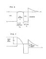
- Fig. 6 is an energy level diagram illustrating a modification of the device of the invention.
- Fig. 7 is a level energy diagram of the device of Fig. 6 under the influence of bias.
- The invention as claimed concerns a semi- conductor device having emitter and collector regions, each forming separated rectifying contact with a base region, said base region having high conductivity and a separation dimension from said emitter to said collector that of the order of the length of the mean free carrier path. It is characterized by said emitter region having in a first section adjacent to an ohmic contact a source of carriers positioning the conduction band of said semiconductor material below the Fermi level in said first section, and in a second section adjacent to said base region providing a barrier of a first magnitude and having a dimension of the order of the length of the mean free path of an electron, and said collector region having a barrier to electron flow of a second magnitude greater than said first magnitude.
- Referring to Fig. 1, a schematic structural illustration of an embodiment of the invention is provided having an
emitter region 1, abase region 2 and acollector region 3, each in turn having respectively an emitter external connection 4, a baseexternal connection 5 and a collectorexternal connection 6. Theemitter region 1 is made up of twosections 7 and 8. The first emitter section 7 serves as a large supply of carriers, is labelled N+ and may be conveniently formed by heavy doping. Thesecond emitter section 8 provides a low barrier to injected carrier flow into thebase region 2. Theemitter section 8 is labelled N- and may be formed by lightly doping within the section defined by the width dimension labelled dEe. - The
base region 2 is made of high conductivity material such as metal having a width in the vicinity of the length of the mean free path of an electron so that carrier transit time and the number of collisions are minimized. - The collector region is made up of a first section 9, labelled N, forming a barrier to carrier flow in the base. The collector barrier is higher than the barrier that is formed by the
emitter section 8. Thecollector region 3 also has asecond collector section 10 labelled N+ which serves to keep the collector resistance and ohmic contact resistance low, and which may be concurrently fabricated by heavier doping. The N, N+ and N- designations in Fig. 1 are provided to indicate relative doping with conductivity type determining impurities. The criteria of thecollector region 3 are satisfied by the Schottky barrier type contact known in the art. - Referring next to Fig. 2 an energy level diagram dimensionally correlated with the structure of Fig. 1 is provided showing in a first portion corresponding to the section 7 of Fig. 1, a condition wherein the conduction band is below the Fermi level thereby providing a large reservoir of carriers. In a second portion corresponding to
section 8 of Fig. 1 as the emitter barrier width labelled dEB, the number of available carriers is reduced such as by light doping. This has the effect that the conduction band then rises and produces barrier height labelled φE. The height of the barrier is controlled by the semiconductor metal interface. It should be noted, however, that for very small values of emitter barrier with the doping level of the reservoir of carriers in section 7 asserts some control. The adjacent highconductivity metal base 2 operates to establish the conduction band at a lower level and reduces the base spreading resistance. - The width of the metal base is in the vicinity of the length of the mean free path of an electron to minimize transit time and number of collisions. The collector barrier height φc is illustrated. The collector barrier height (pc is higher than the emitter barrier height φE. The conduction band then parabolically becomes lower through the Fermi level as a result of the heavy doping of
collector section 10 thereby to reduce collector resistance and minimize contact resistance. - The structure of the invention as described in connection with Figs. 1 and 2 when biased, injects carriers from a large supply over a small barrier where they travel ballistically as hot electrons directly to the collector. The
metal base 2 adjacent to thesection 8 which is a lightly doped thin dimensioned semiconductor section operates to provide a low barrier and an immediate potential drop to an injected carrier. The advantages of a low base spreading resistance with an injection barrier are thus simultaneously provided. - Under conditions of forward bias of the emitter and reverse bias of the collector, the energy level diagram of the device is illustrated in Fig. 3.
- Referring to Fig. 3, in the emitter section 7, a large quantity of carriers is present where the conduction band is lower than the Fermi level. The application of bias shown as VEB produces a potential barrier in the vicinity of the interface of the
thin emitter section 8 while the potential drops toward that of thebase 2. Under these conditions, the carriers once having traversed the barrier now can traverse both the semiconductor region and the base region directly because thesection 8 and thebase 2 are each less than the length of the mean free path of an electron passing over the collector barrier the height of which, φc, has been selected for collection by choice of materials. - Thus the invention operates by providing a large source of carriers impeded by a low thin barrier in the emitter adjacent to a metal base so that having traversed the barrier, the carriers are accelerated by the potential drop toward the base and due to the thin emitter and base regions, transit time to the collector barrier is short.
- Under conditions of a base-emitter bias voltage greater than that which the
thin emitter section 8 will support, it is advisable to operate the device in pulse mode. - The criteria of the structure of the invention can be met in fabrication by a number of semi- conductor process techniques. The technique of molecular beam epitaxy is favored for its controllability.
- Referring next to Fig. 4, an output performance graph is provided illustrating the operating characteristics under the influence of bias in what is known for three-terminal devices as the common base operation. Operating curves labelled a, b and c are provided for three illustrative levels of emitter-base bias VEB. The curve a is for the condition O<VEB<φc/e. The curve b is for the condition VEB+0.1 V. The curve c is for the condition VEB+0.2 V.
- In the graph of Fig. 4 for negative VBC, the various operating curves merge into a single line labelled x, defined by the forward characteristics of the emitter barrier. Similarly, for positive values of VBC the various operational curves merge to a single line labelled y, defined by the breakdown voltage of the reversely biased collector barrier. The slope of the performance curves in the region z closely parallel to the ordinate, are defined by the reverse saturation current of the collector barrier. The load line crosses the operating curves at two points, which when the device is used in a switching mode define the "on" or "off" conditions.
- A dotted line encompasses a range for continuous operation. The continuous operation range is defined by the conditions where the emitter-base bias voltage is greater than the collector barrier height divided by e.
- Referring next to Fig. 5 which illustrates the input characteristics in the common emitter type of circuit operation, the onset of a dynamic negative resistance is observed at the value of VEB equivalent to the collector barrier height divided by e. As the emitter barrier VEB is increased, the base current increases approximately by the 3-halves power of the increase in the emitter base bias until a value of VEB equivalent to the collector barrier height divided by e is reached, in other words IB=IE~VEB 3/2. At this point most of the emitter current will proceed to the collector, the base current will drop and the dynamic negative resistance takes place and the base current then follows a relationship defined by (1-a)IE, the product of the
quantity 1 minus a, and the emitter current. - The device of Fig. 1 has certain features critical to its operation. For
emitter region 1 it is required that there be a first section adjacent to the input terminal that serves as a supplier of carriers, and that there be asemi-conductor section 8 adjacent to a metal base which provides a barrier at the interface with the section 7, and that thesecond section 8 have a very thin dimension. These conditions may be met by constructingsections 7 and 8 using the material GaAs for the section 7 doped to about 5x10¹⁸ and for thesection 8 reducing the doping to about 1015. - The semiconductor material chosen for the
emitter section 8 should have a wide energy gap so that few thermal carriers will exist in the conduction band. - The emitter current density will be space- charge limited for low voltages and obeys an expression known in the art as "Child's Law", as described in
Equation 1. - Equation 1:

- e is the electron charge.
- m* is the electron effective mass.
- The transit time through the emitter region is considered to follow the expression in
Equation 2 for the material GaAs. -

- An example device constructed of the material may be biased under the conditions set forth in Table I.

- Under the conditions of Table I the traverse time (T) through the emitter as determined by
Equation 2 will be 10-13 seconds. The traverse time through the metal base will also be 10-13 seconds where the base width dB is selected to be 100A - The collector barrier is of the type known in the art as a Schottky barrier.
- The equivalent dynamic resistance of the
section 8 of the emitter will follow the expression inEquation 3. -

- The input time constant of the device of the invention using the example GaAs material is in the vicinity of 0.4x10⁻¹³ seconds so that the speed limitation of the device will be determined by the base-collector barrier which in turn responds in the vicinity of 10-13 seconds. The emitter base bias voltage will occur mostly across
section 8, the thin lightly doped region. - Referring next to Fig. 6, a variation in the structure of Fig. 1 can be provided wherein the
section 8 of the emitter region is a semiconductor such as CdS which forms a non-rectifying contact with thebase 2 and the emitter. With such a modification the emitter barrier width should be made wide enough that the accumulation layers which make the semiconductor degenerate on both sides next to the interfaces with the metal will not swamp the total film thickness. This is illustrated by the fact that the conduction band potential level arcs up above the Fermi level inside dEe. For the material CdS, the dimension for the emitter barrier width should increase to about 600A. - Referring next to Fig. 7, an energy diagram is provided under the influence of bias. The bias provides carriers from the metal-emitter contact over the barrier in the non-rectifying semi- conductor and the thin dimensions of both the emitter barrier region and the base permit the carriers to be accelerated directly over the collector barrier without losing any energy due to electron-electron and electron-phonon collisions.
- In both the Fig. 1 and Fig. 6 embodiments, the lightly doped N- section and the non-rectifying semiconductor CdS section are empty of free carriers and thereby support the potential difference VEB. In operation carriers spill over a small barrier at the section 7
section 8 interface or the metal non-rectifying semiconductor CdS interface and then proceed toward the base. Since the thickness of the N- or example CdS section is close to the length of the mean free path of the electrons, they will reach the base with essentially the same energy they were emitted by, which is eVEB, and they will have excess energy above the Fermi level or, in other words, be "hot". - 'Further, since the base is selected to be thin enough, the electrons will traverse it without collisions and maintain their excess energy so as to surmount the collector barrier φc.
- It will also be apparent to one skilled in the art that the base-collector combination 9-10 may be replaced by a metal-oxide-metal contact. Such a structure reduces the transient time through the collector. Similarly the
metal base 2 of Fig. 1 may be replaced by a heavily doped semiconductor. Such a structure will have the advantages of a controllably grown heterojunction of theemitter region 1base region 2 interface thereby reducing some deleterious interface properties such as surface states and defects, and provides a longer mean free path in the epitaxial base. - What has been described is a device wherein a large quantity of carriers and a low barrier emitter region is provided adjacent to a thin high conductivity base such as a metal, so that a quantity of carriers can pass the barrier and traverse the base directly to the collector barrier. Since the structure provides conditions where these carriers do not collide in either the thin barrier region of the emitter region or in the thin base, they maintain a quasi mono-energetic current distribution directly to the collector.
Claims (10)
Applications Claiming Priority (2)
| Application Number | Priority Date | Filing Date | Title |
|---|---|---|---|
| US11817180A | 1980-02-04 | 1980-02-04 | |
| US118171 | 1980-02-04 |
Publications (3)
| Publication Number | Publication Date |
|---|---|
| EP0033496A2 EP0033496A2 (en) | 1981-08-12 |
| EP0033496A3 EP0033496A3 (en) | 1982-04-14 |
| EP0033496B1 true EP0033496B1 (en) | 1985-07-03 |
Family
ID=22376919
Family Applications (1)
| Application Number | Title | Priority Date | Filing Date |
|---|---|---|---|
| EP19810100497 Expired EP0033496B1 (en) | 1980-02-04 | 1981-01-23 | Three-terminal semiconductor device |
Country Status (4)
| Country | Link |
|---|---|
| EP (1) | EP0033496B1 (en) |
| JP (1) | JPS56116672A (en) |
| CA (1) | CA1153825A (en) |
| DE (1) | DE3171163D1 (en) |
Families Citing this family (2)
| Publication number | Priority date | Publication date | Assignee | Title |
|---|---|---|---|---|
| KR200450320Y1 (en) | 2008-05-19 | 2010-09-20 | 김진중 | Read cable connect structure for measuring instrument machine |
| JP5329315B2 (en) * | 2009-06-22 | 2013-10-30 | 日本電信電話株式会社 | Heterojunction bipolar transistor |
Family Cites Families (3)
| Publication number | Priority date | Publication date | Assignee | Title |
|---|---|---|---|---|
| DE1257977B (en) * | 1965-04-17 | 1968-01-04 | Telefunken Patent | Process for manufacturing a metal base transistor |
| US4173763A (en) * | 1977-06-09 | 1979-11-06 | International Business Machines Corporation | Heterojunction tunneling base transistor |
| US4127861A (en) * | 1977-09-26 | 1978-11-28 | International Business Machines Corporation | Metal base transistor with thin film amorphous semiconductors |
-
1980
- 1980-12-22 CA CA000367341A patent/CA1153825A/en not_active Expired
-
1981
- 1981-01-09 JP JP130681A patent/JPS56116672A/en active Granted
- 1981-01-23 DE DE8181100497T patent/DE3171163D1/en not_active Expired
- 1981-01-23 EP EP19810100497 patent/EP0033496B1/en not_active Expired
Also Published As
| Publication number | Publication date |
|---|---|
| JPS56116672A (en) | 1981-09-12 |
| CA1153825A (en) | 1983-09-13 |
| DE3171163D1 (en) | 1985-08-08 |
| JPH0132663B2 (en) | 1989-07-10 |
| EP0033496A3 (en) | 1982-04-14 |
| EP0033496A2 (en) | 1981-08-12 |
Similar Documents
| Publication | Publication Date | Title |
|---|---|---|
| EP0033876B1 (en) | Three-terminal semiconductor device | |
| US4794440A (en) | Heterojunction bipolar transistor | |
| US4758868A (en) | Ballistic hetero-junction transistor with transverse two dimensional electron gas layer | |
| EP0526897A2 (en) | Three terminal tunnel device | |
| US4958208A (en) | Bipolar transistor with abrupt potential discontinuity in collector region | |
| US4825265A (en) | Transistor | |
| CA1245775A (en) | Hot electron unipolar transistor with two- dimensional degenerate electron gas base with continuously graded composition compound emitter | |
| EP0615292A1 (en) | Insulated gate bipolar transistor | |
| US5561306A (en) | Hetero-bipolar transistor having a plurality of emitters | |
| US4903092A (en) | Real space electron transfer device using hot electron injection | |
| US3220896A (en) | Transistor | |
| EP0278386B1 (en) | Heterojunction bipolar transistor | |
| EP0566591A1 (en) | Semiconductor device. | |
| US3250967A (en) | Solid state triode | |
| US4672404A (en) | Ballistic heterojunction bipolar transistor | |
| EP0033496B1 (en) | Three-terminal semiconductor device | |
| US5798539A (en) | Bipolar transistor for very high frequencies | |
| EP0200422B1 (en) | A transistor device | |
| US4449140A (en) | Semi-conductor barrier switching devices | |
| US4910562A (en) | Field induced base transistor | |
| US4829349A (en) | Transistor having voltage-controlled thermionic emission | |
| US3358158A (en) | Semiconductor devices | |
| US3688164A (en) | Multi-layer-type switch device | |
| JPS6124832B2 (en) | ||
| WO1987000692A1 (en) | Semiconductor device |
Legal Events
| Date | Code | Title | Description |
|---|---|---|---|
| PUAI | Public reference made under article 153(3) epc to a published international application that has entered the european phase |
Free format text: ORIGINAL CODE: 0009012 |
|
| AK | Designated contracting states |
Designated state(s): DE FR GB IT |
|
| 17P | Request for examination filed |
Effective date: 19811029 |
|
| PUAL | Search report despatched |
Free format text: ORIGINAL CODE: 0009013 |
|
| AK | Designated contracting states |
Designated state(s): DE FR GB IT |
|
| GRAA | (expected) grant |
Free format text: ORIGINAL CODE: 0009210 |
|
| AK | Designated contracting states |
Designated state(s): DE FR GB IT |
|
| PG25 | Lapsed in a contracting state [announced via postgrant information from national office to epo] |
Ref country code: IT Free format text: LAPSE BECAUSE OF FAILURE TO SUBMIT A TRANSLATION OF THE DESCRIPTION OR TO PAY THE FEE WITHIN THE PRESCRIBED TIME-LIMIT;WARNING: LAPSES OF ITALIAN PATENTS WITH EFFECTIVE DATE BEFORE 2007 MAY HAVE OCCURRED AT ANY TIME BEFORE 2007. THE CORRECT EFFECTIVE DATE MAY BE DIFFERENT FROM THE ONE RECORDED. Effective date: 19850703 |
|
| REF | Corresponds to: |
Ref document number: 3171163 Country of ref document: DE Date of ref document: 19850808 |
|
| ET | Fr: translation filed | ||
| PLBE | No opposition filed within time limit |
Free format text: ORIGINAL CODE: 0009261 |
|
| STAA | Information on the status of an ep patent application or granted ep patent |
Free format text: STATUS: NO OPPOSITION FILED WITHIN TIME LIMIT |
|
| 26N | No opposition filed | ||
| PGFP | Annual fee paid to national office [announced via postgrant information from national office to epo] |
Ref country code: GB Payment date: 19901220 Year of fee payment: 11 |
|
| PGFP | Annual fee paid to national office [announced via postgrant information from national office to epo] |
Ref country code: DE Payment date: 19910131 Year of fee payment: 11 |
|
| PGFP | Annual fee paid to national office [announced via postgrant information from national office to epo] |
Ref country code: FR Payment date: 19911218 Year of fee payment: 12 |
|
| PG25 | Lapsed in a contracting state [announced via postgrant information from national office to epo] |
Ref country code: GB Effective date: 19920123 |
|
| REG | Reference to a national code |
Ref country code: GB Ref legal event code: PCNP |
|
| PG25 | Lapsed in a contracting state [announced via postgrant information from national office to epo] |
Ref country code: DE Effective date: 19921001 |
|
| PG25 | Lapsed in a contracting state [announced via postgrant information from national office to epo] |
Ref country code: FR Effective date: 19930930 |
|
| REG | Reference to a national code |
Ref country code: FR Ref legal event code: ST |