EP0029378B1 - Magnetic domain propagation shift register and memory constituted by these registers - Google Patents
Magnetic domain propagation shift register and memory constituted by these registers Download PDFInfo
- Publication number
- EP0029378B1 EP0029378B1 EP80401566A EP80401566A EP0029378B1 EP 0029378 B1 EP0029378 B1 EP 0029378B1 EP 80401566 A EP80401566 A EP 80401566A EP 80401566 A EP80401566 A EP 80401566A EP 0029378 B1 EP0029378 B1 EP 0029378B1
- Authority
- EP
- European Patent Office
- Prior art keywords
- boxes
- domain
- register
- box
- propagation
- Prior art date
- Legal status (The legal status is an assumption and is not a legal conclusion. Google has not performed a legal analysis and makes no representation as to the accuracy of the status listed.)
- Expired
Links
Images


Classifications
-
- G—PHYSICS
- G11—INFORMATION STORAGE
- G11C—STATIC STORES
- G11C19/00—Digital stores in which the information is moved stepwise, e.g. shift registers
- G11C19/02—Digital stores in which the information is moved stepwise, e.g. shift registers using magnetic elements
- G11C19/08—Digital stores in which the information is moved stepwise, e.g. shift registers using magnetic elements using thin films in plane structure
- G11C19/0866—Detecting magnetic domains
Description
La présente invention concerne un registre à décalage pour mémoire à propagation de domaines magnétiques, comportant une couche magnétique douce dans laquelle s'effectue la propagation des domaines, une couche magnétique dure et un conducteur de décalage des domaines, le canal de propagation des domaines dans la couche douce étant défini par une interruption de la couche dure, et comportant des zones rétrécies de stockage des domaines, des cases élargies de croissance des domaines, une case d'écriture et une case de lecture, et le conducteur de décalage, en forme de grecque, comportant des segments perpendiculaires au canal de propagation.The present invention relates to a shift register for magnetic domain propagation memory, comprising a soft magnetic layer in which the domains are propagated, a hard magnetic layer and a domain shift conductor, the domain propagation channel in the soft layer being defined by an interruption of the hard layer, and comprising narrowed areas for storing the domains, enlarged boxes for growing the domains, a writing box and a reading box, and the offset conductor, in the form Greek, with segments perpendicular to the propagation channel.
Un tel registre est notamment décrit dans la demande de brevet français publiée sous le numéro 2 406 284.Such a register is described in particular in the French patent application published under the
L'invention concerne plus particulièrement la lecture des domaines à l'extrémité aval du canal de propagation des domaines, par exemple par une magnétorésistance de lecture disposée sur la case de lecture du canal de propagation.The invention relates more particularly to the reading of the domains at the downstream end of the domain propagation channel, for example by a reading magnetoresistor placed on the reading box of the propagation channel.
On s'est déjà attaché, dès l'apparition de ces registres à décalage, à obtenir un niveau de lecture qui soit maximal avec, à cet effet, une case de lecture étendue et une structure de registre permettant l'éclatement des domaines et, par conséquent, le remplissage de cette case de lecture avec un domaine également étendu, le niveau de lecture dépendant de la quantité de charges magnétostatiques à l'extrémité aval du domaine. Un registre à décalage utilisant un procédé d'éclatement des domaines afin d'améliorer l'amplitude du signal de lecture est décrit dans la demande de brevet français FR 2 206 558. L'éclatement des domaines, en un nombre déterminé de domaines, selon évidemment l'axe difficile de la couche douce, et donc le remplissage de la case de lecture à partir de plusieurs domaines, présente déjà un avantage. En effet, comme le temps de croissance latérale, c'est-à-dire perpendiculairement à la direction de propagation des domaines, est beaucoup plus long que le temps de croissance des domaines par les pointes, c'est-à-dire dans la direction de propagation des domaines le long de l'axe aisé, le temps de lecture, dans ce cas, comparé à celui qui est nécessaire lorsque la case de lecture n'est remplie qu'à partir d'un seul domaine élargi dans cette case par le conducteur de décalage, est divisé par un nombre égal à la quantité des domaines éclatés.We have already endeavored, as soon as these shift registers appeared, to obtain a maximum reading level with, for this purpose, an extended reading box and a register structure allowing the domains to be broken up and, consequently, the filling of this reading box with an equally extended domain, the reading level depending on the quantity of magnetostatic charges at the downstream end of the domain. A shift register using a domain bursting method in order to improve the amplitude of the read signal is described in French
En outre, l'éclatement des domaines permet de ne pas faire passer le conducteur de décalage, et donc d'élargissement, sur la case de lecture, et de disposer par conséquent la magnétorésistance de lecture sur la case de lecture, au même niveau que le conducteur de décalage.In addition, the bursting of the domains makes it possible not to pass the offset, and therefore widening, conductor over the reading box, and consequently arrange the reading magnetoresistance on the reading box, at the same level as the shift conductor.
Toutefois, cet éclatement des domaines doit s'effectuer par l'intermédiaire de cases d'élargissement. Or la structure des registres connus jusqu'à ce jour était telle qu'on ne pouvait pas envisager l'auto-effacement de ces cases d'élargissement intermédiaires et qu'il fallait prévoir, soit des conducteurs d'effacement, soit et, de préférence, un seul et même conducteur d'effacement mais avec plusieurs passages consécutifs dans le même sens au-dessus de ces cases intermédiaires. Même si le conducteur de décalage servait en même temps de conducteur d'effacement, cela posait un problème de topologie, à cause de l'entourage multiple par le conducteur des plots ou bornes de sortie de celui-ci. De toutes manières, l'accroissement des domaines dans les cases intermédiaires d'élargissement requérait également plusieurs passages consécutifs et dans le même sens du conducteur de décalage, pour préserver la densité de courant le long des cases intermédiaires. Les registres connus posaient donc ce problème de topologie.However, this fragmentation of the domains must be carried out by means of enlargement boxes. However, the structure of the registers known to date was such that one could not envisage the self-erasure of these intermediate enlargement boxes and that it was necessary to provide either erasure conductors or preferably, one and the same erasing conductor but with several consecutive passages in the same direction above these intermediate boxes. Even if the offset conductor simultaneously served as an erasure conductor, this posed a problem of topology, because of the multiple surrounding by the conductor of the pads or output terminals thereof. In any case, increasing the domains in the intermediate widening boxes also required several consecutive passes and in the same direction of the offset conductor, to preserve the current density along the intermediate boxes. The known registers therefore posed this topology problem.
La présente invention vise à éliminer ce problème et, en conséquence, à faciliter la fabrication des registres à propagation de domaines.The present invention aims to eliminate this problem and, consequently, to facilitate the manufacture of domain propagation registers.
A cet effet, la présente invention concerne un registre à décalage pour mémoire à propagation des domaines magnétiques du type défini ci-dessus avec, en amont de la case de lecture, une zone d'élargissement comportant des cases intermédiaires d'élargissement des domaines séparées entre elles, dans le sens de la propagation, par des zones de stockage, caractérisé par le fait que les cases d'élargissement intermédiaires ont une surface importante par rapport à celle des autres cases de croissance et comportent au moins un décrochement latéral, qu'elles ne sont pas recouvertes par le conducteur de décalage, et qu'il est prévu des moyens pour créer, au moins au niveau de la zone d'élargissement et de la case de lecture, un champ magnétique externe pulsé.To this end, the present invention relates to a shift register for propagation memory of magnetic domains of the type defined above with, upstream of the reading box, a widening zone comprising intermediate boxes for widening the separate domains. between them, in the direction of propagation, by storage zones, characterized in that the intermediate enlargement boxes have a large surface area compared to that of the other growth boxes and comprise at least one lateral offset, which they are not covered by the offset conductor, and means are provided for creating, at least at the level of the enlargement zone and the reading box, a pulsed external magnetic field.
Grâce au décrochement des cases d'élargissement intermédiaires qui y crée un champ statique démagnétisant, les domaines magnétiques y sont effacés dans les intervalles de temps où le champ magnétique externe pulsé disparaît. Quant à la propagation et à l'élargissement des domaines dans la zone d'élargissement, c'est précisément ce champ externe qui les assure, les cases d'élargissement n'étant pas soumises à l'action du champ créé par les conducteurs de décalage.Thanks to the unhooking of the intermediate enlargement boxes which creates a demagnetizing static field there, the magnetic domains are erased there in the time intervals when the pulsed external magnetic field disappears. As for the propagation and enlargement of the domains in the enlargement zone, it is precisely this external field which ensures them, the enlargement boxes not being subjected to the action of the field created by the conductors of shift.
La présente invention permet donc avantageusement de dédoubler les fonctions propagation-élargissement des domaines et effacement des domaines.The present invention therefore advantageously makes it possible to split the propagation-enlargement of the domains and erasure of the domains functions.
Par ailleurs, grâce à l'étendue des cases d'élargissement intermédiaires, les champs statiques démagnétisants qui y règnent, tout en étant suffisants pour effacer les domaines, sont toutefois suffisamment faibles pour ne pas s'opposer à la croissance des domaines, notamment dans le sens latéral, sous l'action du champ externe.Furthermore, thanks to the extent of the intermediate enlargement boxes, the demagnetizing static fields which prevail there, while being sufficient to erase the domains, are however sufficiently weak not to oppose the growth of the domains, in particular in the lateral direction, under the action of the external field.
Dans une forme de réalisation préférée du registre de l'invention, lesdits moyens sont agencés pour créer un champ magnétique externe pulsé sur tout le registre.In a preferred embodiment of the register of the invention, said means are arranged to create an external magnetic field pulsed over the entire register.
Dans ce cas, l'invention procure un avantage supplémentaire. En effet, sans champ externe, les domaines ne s'engagent pas complètement dans les zones rétrécies de stockage du canal de propagation.In this case, the invention provides an advantage additional. Indeed, without an external field, the domains do not fully engage in the narrowed storage areas of the propagation channel.
Avec ce champ externe, selon l'invention, les domaines s'étendent jusqu'à l'extrémité aval des zones de stockage. Et lorsque le courant dans le conducteur de décalage s'annule, le champ externe reste encore insuffisant pour faire rentrer le domaine dans les cases de croissance. Ce n'est qu'à l'alternance suivante du courant de décalage que les domaines croissent dans les cases élargies. En conséquence, les domaines transitoires du registre de l'invention sont plus longs que ceux des registres connus, ce qui permet, à structure de registre comparable, d'obtenir une densité de stockage de l'information plus importante.With this external field, according to the invention, the domains extend to the downstream end of the storage areas. And when the current in the offset conductor is canceled, the external field is still insufficient to bring the domain into the growth cells. It is only at the next alternation of the offset current that the domains grow in the enlarged boxes. Consequently, the transient domains of the register of the invention are longer than those of known registers, which makes it possible, with a comparable register structure, to obtain a higher density for storing information.
Les moyens agencés pour créer le champ externe pulsé peuvent être constitués par une bobine plate ou un solénoïde aplati.The means arranged to create the pulsed external field can be constituted by a flat coil or a flattened solenoid.
L'invention sera mieux comprise à la lecture suivante de la description de plusieurs formes de réalisation du registre de l'invention, en référence au dessin annexé, sur lequel :
- La figure 1 est une vue en plan d'une première forme de réalisation du circuit de propagation des domaines du registre de l'invention ;
- la figure 2 est une vue en coupe du canal de propagation du registre de la figure 1 ;
- la figure 3 est une vue en perspective du registre de l'invention avec une bobine plate pour créer un champ externe ;
- la figure 4 est une vue en perspective du registre de l'invention avec un solénoïde aplati pour créer un champ externe ;
- la figure 5 est une vue en plan d'une deuxième forme de réalisation de la zone d'éclatement des domaines du registre de l'invention, et
- la figure 6 est une vue schématique de plusieurs registres selon l'invention, intégrés sur un même substrat.
- Figure 1 is a plan view of a first embodiment of the propagation circuit of the domains of the register of the invention;
- Figure 2 is a sectional view of the propagation channel of the register of Figure 1;
- Figure 3 is a perspective view of the inventive register with a flat coil to create an external field;
- Figure 4 is a perspective view of the inventive register with a flattened solenoid to create an external field;
- FIG. 5 is a plan view of a second embodiment of the bursting area of the domains of the register of the invention, and
- Figure 6 is a schematic view of several registers according to the invention, integrated on the same substrate.
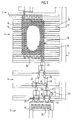
La figure 1 représente unevueen plan du circuit de propagation de domaines dans une première forme de réalisation 1 du registre mémoire de l'invention. Le registre 1 comporte quatre zones successives, à savoir une zone 2 d'écriture des domaines classique, une zone 3 de propagation des domaines, une zone 4 d'élargissement des domaines et une zone 5 de lecture des domaines.FIG. 1 represents a plan view of the domain propagation circuit in a first embodiment 1 of the memory register of the invention. The register 1 comprises four successive zones, namely a
On a représenté, sur la figure 2, une vue en coupe de la zone de propagation 3. Le registre comporte dans cette zone, et de façon connue, un substrat monocristallin 6, ou un autre matériau à surface spéculaire, une couche magnétique douce 7 à anisotropie uniaxiale, une couche magnétique dure 8, déposée en contact intime sur la couche douce 7, sauf le long d'un circuit 11, pour définir dans la couche douce le circuit de propagation 12 des domaines, une couche isolante 9 et une couche conductrice 10, pour le décalage des domaines dans leur circuit de propagation 12. Le conducteur de décalage 10 est disposé en forme de grecque, et comporte ainsi des paires de segments parallèles 13 et 13', destinés à être parcourus en sens inverses par un courant alternatif pulsé de décalage et disposés les uns à côté des autres selon un pas déterminé, sensiblement égal, en l'espèce, à la largeur de ces segments. Le circuit de propagation 12 comporte des segments parallèles à l'axe d'anisotropie uniaxiale de la couche magnétique douce 7, perpendiculaires aux segments du conducteur de décalage, et réunis entre eux deux par des cases ou coudes de repliement 14. Chaque segment du circuit de propagation 12, entre ses deux coudes de repliement d'extrémité, comporte des zones rétrécies 15 de stockage des domaines et des cases élargies 16 de croissance des domaines entre une case de stockage amont et une case de stockage aval, les cases élargies étant disposées alternativement sous les segments 13 et 13' du conducteur de décalage.There is shown in Figure 2, a sectional view of the
Dans la zone 4 d'élargissement des domaines, le registre possède, de façon générale, une structure similaire à celle de la zone de propagation 3 avec, toutefois, les caractéristiques de l'invention suivantes.In the area 4 of enlargement of the domains, the register generally has a structure similar to that of the
Le conducteur de décalage ne comporte plus que quelques paires de segments parallèles 13, 13' espacées entre elles d'un nombre donné de pas des segments conducteurs de la zone de propagation 3. Dans la forme de la réalisation de la figure 1, la zone 4 ne comporte que trois paires de segments conducteurs 13, 13', espacées entre elles deux à deux d'une distance égale à quatre fois le pas des segments de la zone de propagation. Le circuit de propagation des domaines, dans cette zone4, est agencé pour provoquer l'éclatement des domaines en un nombre déterminé de domaines, dans le but d'obtenir un niveau de lecture qui soit maximal. Dans l'exemple représenté, on obtient, à partir d'un domaine, et au bout de six temps d'horloge, quatre domaines qui vont remplir la case de lecture.The offset conductor now only has a few pairs of
Le circuit de propagation de la zone 4 part d'une case rétrécie de stockage des domaines 20 et aboutit à un nombre n donné, en l'espèce 4, de cases de stockage 21, disposées juste en amont de la zone de lecture 5. Entre la case 20 et ces cases 21, le canal de propagation comporte des cases intermédiaires d'élargissement des domaines. Le canal se divise en deux, une première fois, à la sortie de la case de stockage 20, chacun des deux segments du canal issus de cette case 20, se divisant également en deux, à la sortie de cases de stockage 22 situées sous la deuxième paire de segments conducteurs de cette zone 4. Sous chaque paire de segments conducteurs se trouvent, dans le sens de propagation, une première case de stockage, sous le premier segment conducteur, une case de croissance, semblable à celles de la zone de la propagation 3, et une deuxième case de stockage, sous le deuxième segment conducteur. Dans l'exemple représenté, les cases de stockage 22 et 21 sont des dites deuxièmes cases de stockage disposées respectivement sous le deuxième segment conducteur des deuxième et troisième paires de segments conducteurs.The propagation circuit of area 4 starts from a narrowed
Les cases d'élargissement intermédiaires de cette zone 4, de forme générale rectangulaire, présentent trois particularités. En premier lieu, elles sont disposées entre une deuxième case de stockage sous une paire de segments conducteurs et une première case de stockage sous la paire de segments conducteurs suivante, c'est-à-dire qu'elles ne sont pas recouvertes par le conducteur de décalage.The intermediate enlargement boxes of this zone 4, of generally rectangular shape, have three particularities. First, they are arranged between a second storage box under a pair of conductive segments and a first storage box under the next pair of conductive segments, that is to say that they are not covered by the conductor. offset.
En second lieu, elles comportent au moins un décrochement latéral, dans la direction perpendiculaire au sens de propagation. On a ainsi prévu des cases d'élargissement intermédiaires sim- pies 23, entre la première et la deuxième paire de segments conducteurs, comportant un seul décrochement latéral 24 et, par conséquent, une seule sortie sur une seule première case de stockage rétrécie 25, et des cases d'élargissement intermédiaires doubles 26, une juste en amont de la première paire de segments conducteurs, et deux entre les deuxième et troisième paires de segments conducteurs, comportant chacune deux décrochements latéraux 27, 28 en sens opposés, et par conséquent deux sorties sur deux premières cases de stockage rétrécies 29, 30.Secondly, they comprise at least one lateral offset, in the direction perpendicular to the direction of propagation. Simple
Dans la forme de réalisation de la figure 1, les décrochements 24, 27, 28 sont tels que les cases d'élargissement possèdent des petits côtés, perpendiculaires à l'axe aisé de la couche magnétique douce, sur lesquels s'accumulent des charges magnétostatiques négatives, sur les côtés amont, et des charges magnétostatiques positives, sur les côtés aval. Ces charges créent dans les cases 23 et 26 un champ statique démagnétisant.In the embodiment of FIG. 1, the
Enfin, les cases d'élargissement intermédiaires ont une surface importante, comparativement à celle des cases de croissance, de cette zone et de la zone de propagation 3.Finally, the intermediate enlargement boxes have a large surface area, compared to that of the growth boxes, this zone and the
En aval de la zone d'élargissement 4 précédemment décrite, se situe la zone de lecture 5, comportant une très grande case de lecture 31, raccordée aux quatre sorties 21 de la zone 4 par quatre cases de croissance 32, et une magnétorésistance de lecture 33, disposée directement sur la case 31, au même niveau que le conducteur de décalage 10, celui-ci ne passant pas sur la case de lecture.Downstream of the enlargement zone 4 described above, there is the
Le conducteur de décalage étant, de façon connue en soi, parcouru par des impulsions de courant pour créer un champ magnétique « interne », il est prévu, conformément à l'invention, de superposer à ce champ interne un champ magnétique externe pulsé, parallèle à la direction de propagation des domaines.The offset conductor being, in a manner known per se, traversed by current pulses to create an “internal” magnetic field, it is planned, according to the invention, to superimpose on this internal field a pulsed, parallel external magnetic field to the direction of domain propagation.
Ainsi, on a prévu dans la forme de réalisation de la figure 3, de créer ce champ auxiliaire en envoyant un courant pulsé, de même signe, dans une bobine plate 40, située en dessous du substrat mémoire 6. La bobine 40 est constituée d'un conducteur déposé sur un substrat de céramique 41, sur lequel on a également déposé les plots de reprise de contact 42 (non représentés sur la figure 1) du conducteur 10 qui est déposé sur le substrat mémoire 6. La réalisation de la bobine 40 est économique, car elle ne requiert ni assemblage, ni étape de fabrication supplémentaire. Le substrat 41 de la bobine est disposé dans une embase de boîtier 43.Thus, in the embodiment of FIG. 3, provision has been made to create this auxiliary field by sending a pulsed current, of the same sign, into a
Dans la forme de réalisation de la figure 4, le champ magnétique auxiliaire externe est créé par un petit solénoïde aplati 50 entourant le substrat mémoire 6. La fabrication de ce solénoïde est également économique et on peut facilement et directement faire passer les connexions des plots du substrat mémoire à travers les deux ouvertures du solénoïde.In the embodiment of FIG. 4, the external auxiliary magnetic field is created by a small flattened
On a vu plus haut que le champ auxiliaire externe était parallèle à la direction de propagation des domaines. Bien qu'il ne s'agisse pas d'une condition impérative, il est toutefois préférable de la respecter pour éviter les nucléations parasites.We saw above that the external auxiliary field was parallel to the direction of propagation of the domains. Although it is not an imperative condition, it is however preferable to respect it to avoid parasitic nucleations.
Le registre de l'invention ayant maintenant été décrit, on peut aborder les aspects essentiels de son fonctionnement.The register of the invention having now been described, one can approach the essential aspects of its operation.
Comme on l'a vu plus haut, les décrochements 24, 27 et 28 créent dans les cases intermédiaires d'élargissement des domaines 23 et 26 un champ statique démagnétisant. Dans les intervalles de temps où le champ externe pulsé, créé par la bobine 40, ou le solénoïde 50, disparaît, les domaines magnétiques y sont effacés. Lorsque ce champ magnétique externe n'est pas nul, c'est lui qui assure, dans la zone 4 d'éclatement des domaines, la propagation et l'élargissement des domaines magnétiques, les cases d'élargissement 23 et 26 n'étant pas recouvertes par le conducteur de décalage 10, et n'étant pas, de ce fait, soumises au champ magnétique créé par ce conducteur.As we saw above, the
La présente invention permet donc de séparer, dans la zone d'éclatement des domaines, les fonctions propagation-élargissement, d'une part, et effacement, d'autre part. Il faut noter que, grâce à l'étendue des cases intermédiaires 23 et 26, les champs statiques démagnétisants qui y règnent, tout en étant suffisants pour effacer les domaines, sont toutefois insuffisants pour s'opposer à la croissance des domaines sous l'action du champ auxiliaire.The present invention therefore makes it possible to separate, in the burst zone of the domains, the propagation-enlargement functions, on the one hand, and erasure, on the other hand. It should be noted that, thanks to the extent of the
Grâce au champ magnétique externe créé par la bobine40, ou le so!énoïde50. sur tout le registre 1, les domaines s'étendent jusqu'à l'extrémité aval des cases de stockage 15. Et lorsque le courant dans le conducteur de décalage 10 s'annule, le champ auxiliaire externe reste insuffisant pour faire entrer les domaines dans les cases de croissance 16. Ce n'est qu'à l'alternance suivante du courant dans le conducteur 10 que les domaines croissent dans les cases 16. En conséquence, ces domaines transitoires sont très longs, ce qui permet d'obtenir une densité de stockage de l'information très importante.Thanks to the external magnetic field created by the
A titre d'exemple, on peut réaliser la bobine 40, ou le solénoïde 50, avec des conducteurs disposés selon un pas de 50 à 100 µm. Avec une amplitude de courant de 100 mA, on crée un champ auxiliaire externe de 12 Oersted. Pour une couche magnétique douce 7 de 1 500 Â d'épaisseur en alliage amorphe de Nl50CO40P10, déposée chimiquement sans courant en voie humide, avec une densité d'énergie de parois de 1,7 erg/cm2, on réalise un registre 1 selon l'invention possédant une densité de 130 000 bits/cm2. A partir d'un alliage sensiblement différent et une épaisseur plus faible, la densité peut être supérieure à 250000 bits/cm2. La magnétorésistance 33 est constituée par un conducteur également en forme de grecque, an alliage de Nias" Fel4, de 2 000 Â d'épaisseur. La lecture de la case 31 est effectuée en 0,5 µs. Pendant un temps d'horloge de 1 lis, on effectue une écriture dans la zone du registre 1, une lecture dans la zone 5, et toute l'information contenue dans le registre 1 se décale d'un pas.For example, one can make the
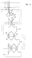
La structure du registre 1, telle qu'elle est décrite ci-dessus, est particulièrement adaptée pour l'intégration complète d'une mémoire, avec ses circuits d'accès (générateur de courant d'écriture, générateur ou interrupteur de courant de décalage, amplificateur de lecture, logique de contrôle), sur une pastille monolithique de circuit intégré classique. Cette intégration peut être effectuée sur tranche de silicium, corindon, etc., en déposant d'abord les circuits d'accès sur cette tranche de semi-conducteur, en les protégeant ensuite, par exemple par une couche de verre, puis en déposant la structure magnétique sur la même tranche, de la manière décrite ci-dessus. La forme de réalisation de la figure 5 de la zone d'éclatement des domaines diffère de celle de la figure 1. Elle permet d'éviter un risque et présente un avantage supplémentaire.The structure of register 1, as described above, is particularly suitable for the complete integration of a memory, with its access circuits (write current generator, generator or shift current switch , reading amplifier, control logic), on a monolithic pad of a conventional integrated circuit. This integration can be carried out on a silicon wafer, corundum, etc., by first depositing the access circuits on this semiconductor wafer, then protecting them, for example with a layer of glass, then depositing the magnetic structure on the same wafer, as described above. The embodiment of FIG. 5 of the bursting area of the domains differs from that of FIG. 1. It makes it possible to avoid a risk and has an additional advantage.
Tout d'abord, les petits côtés décrochés des cases d'élargissement 23 et 26 de la première forme de réalisation décrite, sur lesquels s'accumulent les charges magnétostatiques, sont relativement longs par rapport aux côtés correspondants des autres cases de croissance du registre. Il en résulte un risque de nucléation des domaines, que la forme de réalisation de la figure 5 élimine. En effet, les décrochements latéraux de cette forme-ci, au lieu d'être perpendiculaires sur toute leur longueur à l'axe aisé de la couche magnétique douce, comme ceux de la figure 1, ont une forme générale courbe et se raccordent progressivement à une case élargie classique, en amont ou en aval de celle-ci suivant le décrochement considéré, en faisant un angle relativement faible avec la direction d'anisotropie de la couche douce. L'angle optimal de raccordement est voisin de 30°. Toutefois, pour qu'un champ démagnétisant soit créé dans ces cases d'élargissement, pour l'effacement des domaines, il est nécessaire de former localement de petits décrochements véritablement perpendiculaires à la direction d'anisotropie, pour que des charges magnétostatiques s'y accumulent.First, the short sides of the
Ainsi, la zone d'éclatement des domaines de la figure 5 part d'une case élargie classique 60 et aboutit à quatre cases élargies classiques 61. Entre ces cases, le canal de propagation se divise une première fois en deux, à la sortie de la première grande case d'élargissement 62, pour aboutir à deux cases élargies classiques 63. En aval des cases 63, le canal de propagation se divise une seconde fois en trois, à la sortie de la deuxième grande case d'élargissement 64, pour aboutir à trois cases élargies classiques 65. Enfin, entre les cases 65 et 61, le canal de propagation comporte une troisième grande case d'élargissement 66, à quatre sorties, qui vont remplir la case de lecture 67.Thus, the bursting area of the domains of FIG. 5 starts from a conventional
L'une des particularités de cette zone d'éclatement, comme on l'a vu plus haut, réside dans le fait que chaque décrochement latéral, par exemple le décrochement 68 de la case 62, est en réalité constitué par une série de petits décrochements 69 perpendiculaires à la direction d'anisotropie et décalés dans le sens de propagation des domaines, pour former une ligne courbe progressive 70 faisant un angle a assez faible avec la direction d'anisotropie 71. A chaque case élargie classique sont raccordés deux décrochements progressifs amont et deux décrochements progressifs aval.One of the peculiarities of this bursting zone, as we saw above, resides in the fact that each lateral step, for example the
La seconde particularité de la zone d'éclatement de la figure 5 réside dans le fait que chaque case élargie classique 60, 63, 65 et 61 est associée, en amont, à une case rétrécie de stockage normale 80 et, en aval, à une case rétrécie 81 trop courte pour conserver les domaines, contrairement aux cases rétrécies aval de la figure 1. Il en résulte l'avantage, outre l'élimination de tout danger de nucléation de domaines, que les domaines ne sont plus bloqués à l'entrée des grandes cases d'élargissement des domaines, c'est-à-dire en aval des cases élargies classiques, et qu'on élimine ainsi un passage de conducteur de décalage, en l'espèce celui qui, dans la forme de réalisation de la figure 1, passait au-dessus des cases rétrécies de stockage situées en aval des cases élargies classiques.The second peculiarity of the bursting area of FIG. 5 lies in the fact that each conventional
Grâce à la forme de réalisation de la zone d'éclatement de la figure 5, il est tout à fait possible, selon le schéma de la figure 6, d'intégrer plusieurs registres 90, 91, 92, par exemple, sur un même substrat, en imbriquant leurs zones d'éclatement les unes dans les autres, et en ne formant qu'une seule zone de lecture, avec une seule case de lecture 93, et par conséquent une seule magnétorésistance de lecture. Cette intégration procure un gain de place important. On peut aussi fabriquer une mémoire de 64 k, avec 16 registres de 4 k, ou de 256 k, avec 32 registres de 8 k.Thanks to the embodiment of the burst zone of FIG. 5, it is quite possible, according to the diagram of FIG. 6, to integrate
Claims (12)
Applications Claiming Priority (2)
| Application Number | Priority Date | Filing Date | Title |
|---|---|---|---|
| FR7927447 | 1979-11-07 | ||
| FR7927447A FR2469776A1 (en) | 1979-11-07 | 1979-11-07 | SHIFT REGISTER FOR MAGNETIC DOMAIN PROPAGATION MEMORY |
Publications (2)
| Publication Number | Publication Date |
|---|---|
| EP0029378A1 EP0029378A1 (en) | 1981-05-27 |
| EP0029378B1 true EP0029378B1 (en) | 1982-12-15 |
Family
ID=9231387
Family Applications (1)
| Application Number | Title | Priority Date | Filing Date |
|---|---|---|---|
| EP80401566A Expired EP0029378B1 (en) | 1979-11-07 | 1980-11-03 | Magnetic domain propagation shift register and memory constituted by these registers |
Country Status (5)
| Country | Link |
|---|---|
| US (1) | US4419742A (en) |
| EP (1) | EP0029378B1 (en) |
| JP (1) | JPS5927035B2 (en) |
| DE (1) | DE3061365D1 (en) |
| FR (1) | FR2469776A1 (en) |
Families Citing this family (1)
| Publication number | Priority date | Publication date | Assignee | Title |
|---|---|---|---|---|
| DE19637356C1 (en) * | 1996-09-13 | 1998-01-22 | Payen Goetze Gmbh | Laminated flat metal gasket for cylinder-head of internal combustion engine |
Family Cites Families (4)
| Publication number | Priority date | Publication date | Assignee | Title |
|---|---|---|---|---|
| FR2206558B2 (en) * | 1972-11-16 | 1977-08-05 | Tecsi | |
| FR2263579B2 (en) * | 1974-03-08 | 1976-12-10 | Tecsi Tech Systemes Inf | |
| FR2346807A1 (en) * | 1976-04-01 | 1977-10-28 | Crouzet Sa | MEMORY FOR PROPAGATION OF SINGLE-LAYER DOMAINS OF CONDUCTORS |
| FR2406284A1 (en) * | 1977-10-12 | 1979-05-11 | Crouzet Sa | REGISTER FOR DOMAIN PROPAGATION MEMORIES |
-
1979
- 1979-11-07 FR FR7927447A patent/FR2469776A1/en active Granted
-
1980
- 1980-10-29 US US06/201,738 patent/US4419742A/en not_active Expired - Lifetime
- 1980-11-03 DE DE8080401566T patent/DE3061365D1/en not_active Expired
- 1980-11-03 EP EP80401566A patent/EP0029378B1/en not_active Expired
- 1980-11-07 JP JP55156040A patent/JPS5927035B2/en not_active Expired
Also Published As
| Publication number | Publication date |
|---|---|
| JPS5927035B2 (en) | 1984-07-03 |
| JPS5674887A (en) | 1981-06-20 |
| FR2469776A1 (en) | 1981-05-22 |
| FR2469776B1 (en) | 1984-03-09 |
| EP0029378A1 (en) | 1981-05-27 |
| US4419742A (en) | 1983-12-06 |
| DE3061365D1 (en) | 1983-01-20 |
Similar Documents
| Publication | Publication Date | Title |
|---|---|---|
| EP0677838B1 (en) | Magnetic head matrix device, especially made of thin layers | |
| EP2599138B1 (en) | Writeable magnetic element | |
| EP2633525B1 (en) | Writable magnetic element | |
| EP2047489B1 (en) | Thin-layered magnetic device with high spin polarization perpendicular to the plane of the layers, and magnetic tunnel junction and spin valve using such a device | |
| CA2553577A1 (en) | Magnetic memory with a magnetic tunnel junction written in a thermally assisted manner, and method for writing the same | |
| FR3077917A1 (en) | MAGNETIC STACK, JUNCTION TUNNEL, MEMORY POINT AND SENSOR COMPRISING SUCH A STACK | |
| FR2892231A1 (en) | MAGNETIC DEVICE WITH MAGNETORESISTIVE TUNNEL JUNCTION AND MAGNETIC MEMORY WITH RANDOM ACCESS | |
| EP0436424B1 (en) | Magnetooptical read head | |
| WO2006064022A1 (en) | Spin-electronics device | |
| EP2255362A1 (en) | Magnetic member with thermally assisted writing | |
| FR2549630A1 (en) | OPTICO-MAGNETIC RECORDING MEDIUM | |
| EP0029378B1 (en) | Magnetic domain propagation shift register and memory constituted by these registers | |
| EP0433174B1 (en) | Integrated circuit with complete protection against ultraviolet rays | |
| EP0497069B1 (en) | Magnetoresistive sensor fabrication method and magnetic device produced according to such a method | |
| EP0434547B1 (en) | Multitrack magnetic read head | |
| FR2944910A1 (en) | VORTEX MAGNETIC MEMORIZATION DEVICE | |
| FR2468183A1 (en) | INTEGRATED MAGNETIC TRANSDUCER | |
| EP0409673B1 (en) | Integrated magnetic recording head | |
| EP0132186A1 (en) | Highly integrated magnetic transducer for writing information on a magnetic carrier | |
| WO2000059051A1 (en) | Microelectronic device with tunnel junctions, memory network sensor comprising such devices | |
| FR2604283A1 (en) | Ferroelectric polymeric memory | |
| EP4369884A1 (en) | Three-dimensional structure of nor-type memories | |
| EP0203849B1 (en) | Magnetic bubble generator for a hybrid-technology bubble memory | |
| EP1271547A1 (en) | Semiconductor device and DRAM | |
| EP0394082A1 (en) | Sensing device for magnetic bubble memory |
Legal Events
| Date | Code | Title | Description |
|---|---|---|---|
| PUAI | Public reference made under article 153(3) epc to a published international application that has entered the european phase |
Free format text: ORIGINAL CODE: 0009012 |
|
| AK | Designated contracting states |
Designated state(s): DE GB IT NL |
|
| 17P | Request for examination filed |
Effective date: 19810727 |
|
| ITF | It: translation for a ep patent filed |
Owner name: CALVANI SALVI E VERONELLI S.R.L. |
|
| GRAA | (expected) grant |
Free format text: ORIGINAL CODE: 0009210 |
|
| AK | Designated contracting states |
Designated state(s): DE GB IT NL |
|
| REF | Corresponds to: |
Ref document number: 3061365 Country of ref document: DE Date of ref document: 19830120 |
|
| PGFP | Annual fee paid to national office [announced via postgrant information from national office to epo] |
Ref country code: DE Payment date: 19850131 Year of fee payment: 5 |
|
| PGFP | Annual fee paid to national office [announced via postgrant information from national office to epo] |
Ref country code: NL Payment date: 19861130 Year of fee payment: 7 |
|
| PG25 | Lapsed in a contracting state [announced via postgrant information from national office to epo] |
Ref country code: NL Effective date: 19880601 |
|
| NLV4 | Nl: lapsed or anulled due to non-payment of the annual fee | ||
| GBPC | Gb: european patent ceased through non-payment of renewal fee | ||
| PG25 | Lapsed in a contracting state [announced via postgrant information from national office to epo] |
Ref country code: DE Effective date: 19880802 |
|
| PG25 | Lapsed in a contracting state [announced via postgrant information from national office to epo] |
Ref country code: GB Effective date: 19881118 |
|
| PLBE | No opposition filed within time limit |
Free format text: ORIGINAL CODE: 0009261 |
|
| STAA | Information on the status of an ep patent application or granted ep patent |
Free format text: STATUS: NO OPPOSITION FILED WITHIN TIME LIMIT |