EP0028743B1 - Circuit for generating a sine wave from a triangular wave - Google Patents
Circuit for generating a sine wave from a triangular wave Download PDFInfo
- Publication number
- EP0028743B1 EP0028743B1 EP80106510A EP80106510A EP0028743B1 EP 0028743 B1 EP0028743 B1 EP 0028743B1 EP 80106510 A EP80106510 A EP 80106510A EP 80106510 A EP80106510 A EP 80106510A EP 0028743 B1 EP0028743 B1 EP 0028743B1
- Authority
- EP
- European Patent Office
- Prior art keywords
- differential amplifiers
- differential
- differential amplifier
- signal
- circuit
- Prior art date
- Legal status (The legal status is an assumption and is not a legal conclusion. Google has not performed a legal analysis and makes no representation as to the accuracy of the status listed.)
- Expired
Links
Images


Classifications
-
- H—ELECTRICITY
- H03—ELECTRONIC CIRCUITRY
- H03B—GENERATION OF OSCILLATIONS, DIRECTLY OR BY FREQUENCY-CHANGING, BY CIRCUITS EMPLOYING ACTIVE ELEMENTS WHICH OPERATE IN A NON-SWITCHING MANNER; GENERATION OF NOISE BY SUCH CIRCUITS
- H03B28/00—Generation of oscillations by methods not covered by groups H03B5/00 - H03B27/00, including modification of the waveform to produce sinusoidal oscillations
Definitions
- the present invention relates to a circuit for generating a sinusoidal signal from a linearly rising or falling signal using the non-linear characteristic of a first transistor differential amplifier, to which two additional differential amplifiers are connected in parallel on the output side, the characteristic slope of which is opposite to that of the first differential amplifier.
- a circuit for generating a sine curve from an input signal corresponding to the phase angle is known from " Electronics Letters", August 18, 1977, Vol. 13, No. 17, pp. 506 to 508.
- Differential amplifiers connected in parallel are also used.
- the characteristic curves of these differential amplifiers are alternately positive and negative and offset by corresponding bias voltages on a transistor base of each differential amplifier in such a way that the resulting characteristic curve approximates a sine curve with several periods.
- the more differential amplifiers used the weaker the kinks in the amplitude maxima and minima. A sufficient flattening of these kinks requires a relatively large number of differential amplifiers.
- the invention has for its object to provide a circuit of the type mentioned, with the use of only three differential amplifiers from a triangular wave a sine wave without kinks, with low distortion and high accuracy can be generated.
- the linearly increasing or decreasing signal is a triangular signal, in that the two transistor bases of the first differential amplifier are connected to a transistor base of each additional differential amplifier, and the other transistor bases of each additional differential amplifier are connected to one another and are connected to a common current source and that the bases of all transistors of the differential amplifiers are connected via ground resistors with ground potential and the emitters of all these transistors are connected via emitter resistors to the current sources assigned to the differential amplifiers, the values of the base and emitter resistors and of the current sources being chosen in this way that the resulting characteristic of the circuit has the slope zero at the maximum amplitude of the triangular signal.
- the circuit according to the invention delivers a sine wave of very good quality with relatively little circuit complexity. It can also be implemented with very fast switching elements and, if required, as an integrated circuit and is therefore also suitable for generating sine waves at very high frequencies.
- the circuit shown in Fig. 1 is divided into three main parts, namely a sine shaper 1, an input multiplier 2 and an output multiplier 3.
- the sine shaper 1 in turn has three differential amplifiers 11, 12 and 13, the operation of which is explained below.
- the input multiplier 2 has two npn transistors T, and T z , the emitters of which are connected to a common current source I T.
- the bases of the transistors T 1 and T z are connected to ground on the one hand via diodes D 1 and D z and on the other hand to input terminals 15 and 17, respectively the.
- Input currents I E ⁇ X and I E ⁇ (1-X) are fed to input terminals 15 and 17.
- II E is constant, X is the variation of the input current, so in the present case it has a triangular shape.
- the input multiplier 2 serves to convert the temperature-independent input current into a temperature-dependent one.
- the current source I T is therefore constructed in such a way that it emits a current which is proportional to the absolute temperature.
- the output currents of the input multiplier 2 are now I T ⁇ (1-X) and I T ⁇ X and are therefore also proportional to the absolute temperature.
- the collectors of the transistors T 1 and T 2 carrying these currents are connected to circuit points A and B, which are connected to ground via resistors R o and between which a voltage drop proportional to the absolute temperature arises.
- the node A is also connected to the base of an npn transistor T 3 of the differential amplifier 11 and to the base of an npn transistor T 6 , which belongs to the differential amplifier 12.
- the circuit point B is connected to the base of the other npn transistor T 4 of the differential amplifier 11 and to the base of an npn transistor T, which belongs to the differential amplifier 13.
- K B is an empirically determined constant (see below).
- the differential amplifier 11 is the main former, while the differential amplifiers 12 and 13 serve to correct its characteristic curve in such a way that the oscillation obtained has no discontinuities in its slope.
- the differential amplifier 11 also has two diodes D 3 and D 4 , via which the emitters of the two transistors T 3 and T 4 are connected to a common current source I T K. Path, line and discrete emitter resistances of the individual differential amplifiers 11, 12 and 13 are represented schematically by resistors R.
- the emitters of the transistors T 5 and T 6 as well as T 7 and T a are each connected to a current source I T K 2 .
- K 1 and K 2 are constants to be determined empirically (see below).
- U T is the so-called temperature voltage, which is proportional to the absolute temperature (in the present example, all transistors are of the same type.
- Z 1 , Z 2 and Z 3 are variable coefficients similar to X at the input of the sine shaper 1.
- the collectors of the transistors T 3 , T 6 and T 7 on the one hand and of the transistors T 4 , T 6 and T 8 on the other hand are connected to one another and emit the total currents I s and I s .
- the currents I s and I s are already sinusoidal, but are still temperature-dependent. This temperature dependency is eliminated by means of the output multiplier 3.
- the bases of the transistors T 9 and T 1 are connected to ground on the one hand via diodes D 5 and D 6 and on the other hand to the outputs of the sinusoidal shaper 1 carrying the currents I s and Is.
- the output currents of the output multiplier 3 at terminals 19 and 21 are I A ⁇ Y and I A ⁇ (1-Y). Y is the sinusoidally variable coefficient.
- X is between 0.25 and 0.75 and I T is 10 mA at 25 ° C.
- I T is 10 mA at 25 ° C.
- the output signals at terminals 19 and 21 of the circuit according to FIG. 1 are independent of temperature.
- equations 1 through 3 the left sides and on the right sides both the logarithmic term and the linear term are proportional to the absolute temperature. This also applies to the currents I s and I s , as already mentioned above. The temperature independence is then compensated in the output multiplier 3.
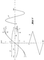
- FIG. 2 shows how the resulting characteristic curve of the sine shaper 1 according to FIG. 1 is composed.
- 31 designates the triangular oscillation which forms the input signal U AB of the sine shaper 1.
- the characteristic curve of the differential amplifier 11 is designated by 33. It can be seen that the characteristic curve 33 approaches a horizontal asymptote for large positive and negative voltages U AB , but that its slope does not become zero. However, the latter can be achieved by linearly superimposing the characteristic curves 35 and 37 of the differential amplifiers 12 and 13 (FIG. 1), as can be seen from the diagram according to FIG. 2.
- the resulting characteristic curve is designated 39.
- Curve 41 is the output sine wave of the differential current I s -I s as a function of phase angle.
- 1 1 , I 2 and 1 3 mean the differential currents of the individual differential amplifiers 11, 12 and 13, respectively
- FIG. 3 shows the deviation of the sine curve 41 (FIG. 2) from the ideal sine shape in the present exemplary embodiment.
- 43 is the error curve. It can be seen that the error is a maximum of ⁇ 2.2 ⁇ .
- the degree of distortion is 60 dB.
- the circuit described above is suitable for frequencies up to 100 MHz (transit frequency 1 GHz).
Landscapes
- Engineering & Computer Science (AREA)
- Power Engineering (AREA)
- Theoretical Computer Science (AREA)
- Amplifiers (AREA)
Description
Die vorliegende Erfindung betrifft eine Schaltung zur Erzeugung eines Sinussignals aus einem linear ansteigenden bzw. abfallenden Signal unter Ausnutzung der nichtlinearen Kennlinie eines ersten Transistordifferenzverstärkers, zu welchem zwei zusätzliche Differenzverstärker ausgangsseitig parallelgeschaltet sind, deren Kennliniensteigungen der des ersten Differenzverstärkers entgegengesetzt sind.The present invention relates to a circuit for generating a sinusoidal signal from a linearly rising or falling signal using the non-linear characteristic of a first transistor differential amplifier, to which two additional differential amplifiers are connected in parallel on the output side, the characteristic slope of which is opposite to that of the first differential amplifier.
Es ist bekannt, eine Sinusschwingung aus einer Dreiecksschwingung unter Verwendung eines Diodennetzwerks zu erzeugen. Ein solches Diodennetzwerk wandelt die ansteigende und die abfallende Rampe der Dreiecksschwingung derart in Geradenabschnitte um, dass eine Sinuskurve angenähert wird. Es ist offensichtlich, dass für eine möglichst genaue Annäherung der Sinuskurve sehr viele Geradenabschnitte benötigt werden, was wiederum zu einem erheblichen Schaltungsaufwand führt.It is known to generate a sine wave from a triangular wave using a diode network. Such a diode network converts the rising and falling ramp of the triangular wave into straight sections in such a way that a sine curve is approximated. It is obvious that a very large number of straight line sections are required for the most accurate approximation of the sine curve, which in turn leads to a considerable amount of circuitry.
Es ist auch bekannt ("IEEE Journal of Solid-State Circuits", Juni 1976, S. 418 ff.), die nichtlineare Kennlinie eines Transistordifferenzverstärkers zur Umwandlung einer Dreieckskurve in eine Sinuskurve zu benutzen. Obwohl sich hierdurch eine Sinusschwingung mit relativ geringem Klirrfaktor erzeugen lässt, haftet ihr doch der Nachteil an, dass sie im Amplitudenmaximum bzw. -minimum einen Knick aufweist. Dies rührt daher, dass die nichtlineare Kennlinie des Differenzverstärkers selbst nicht in die Steigung Null ausläuft, sondern sich ihr nur asymptotisch nähert.It is also known ( " IEEE Journal of Solid-State Circuits", June 1976, p. 418 ff.) To use the nonlinear characteristic of a transistor differential amplifier for converting a triangular curve into a sine curve. Although this enables a sine wave with a relatively low distortion factor to be generated, it suffers from the disadvantage that it has a kink in the amplitude maximum or minimum. This is due to the fact that the non-linear characteristic of the differential amplifier itself does not end in the slope zero, but only approaches it asymptotically.
Bei einer anderen bekannten Schaltung (DE-OS Nr. 2613338) wird das Dreieckssignal parallel auf zwei Differenzverstärker gegeben, von denen einer eine nichtlineare und der andere eine lineare Kennlinie aufweist. Die Ausgangssignale dieser beiden Differenzverstärker werden voneinander subtrahiert. Die Gesamtschaltung hat dadurch eine Kennlinie, deren Steigung den Wert Null durchläuft und dann negativ wird. Wird sie genau bis zu den Punkten ausgesteuert, wo die Steigung Null ist, so entsteht eine Sinuskurve, deren Steigung keine Unstetigkeiten aufweist. Nachteilig bei dieser Schaltung ist jedoch die Differenzbildung, die nach den bekannten Regeln der Fehlerrechnung zu relativ grossen Fehlern im Ausgangssignal führen kann.In another known circuit (DE-OS No. 2613338), the triangular signal is applied in parallel to two differential amplifiers, one of which has a nonlinear characteristic and the other a linear characteristic. The output signals of these two differential amplifiers are subtracted from each other. The overall circuit thus has a characteristic curve whose slope passes through the value zero and then becomes negative. If it is driven exactly to the points where the slope is zero, a sine curve is created, the slope of which has no discontinuities. A disadvantage of this circuit, however, is the difference formation, which, according to the known rules of error calculation, can lead to relatively large errors in the output signal.
Aus "Electronics Letters", 18. August 1977, Bd. 13, Nr. 17, S. 506 bis 508, ist eine Schaltung zur Erzeugung einer Sinuskurve aus einem dem Phasenwinkel entsprechenden Eingangssignal bekannt. Dabei werden ebenfalls parallelgeschaltete Differenzverstärker benutzt. Die Kennlinien dieser Differenzverstärker sind abwechselnd positiv und negativ und durch entsprechende Vorspannungen an jeweils einer Transistorbasis jedes Differenzverstärkers so versetzt, dass die resultierende Kennlinie eine Sinuskurve mit mehreren Perioden approximiert. Je mehr Differenzverstärker dabei verwendet werden, desto schwächer werden auch die Knicke in den Amplitudenmaxima bzw. -minima. Eine hinreichende Abflachung dieser Knicke erfordert aber relativ viele Differenzverstärker.A circuit for generating a sine curve from an input signal corresponding to the phase angle is known from " Electronics Letters", August 18, 1977, Vol. 13, No. 17, pp. 506 to 508. Differential amplifiers connected in parallel are also used. The characteristic curves of these differential amplifiers are alternately positive and negative and offset by corresponding bias voltages on a transistor base of each differential amplifier in such a way that the resulting characteristic curve approximates a sine curve with several periods. The more differential amplifiers used, the weaker the kinks in the amplitude maxima and minima. A sufficient flattening of these kinks requires a relatively large number of differential amplifiers.
Der Erfindung liegt die Aufgabe zugrunde, eine Schaltung der eingangs genannten Art zu schaffen, mit der bei Verwendung von lediglich drei Differenzverstärkern aus einer Dreiecksschwingung eine Sinusschwingung ohne Knicke, mit geringem Klirrfaktor und hoher Genauigkeit erzeugbar ist. Diese Aufgabe wird erfindungsgemäss unter der Voraussetzung, dass das linear ansteigende bzw. abfallende Signal ein Dreieckssignal ist, dadurch gelöst, dass die beiden Transistorbasen des ersten Differenzverstärkers mit je einer Transistorbasis jedes zusätzlichen Differenzverstärkers verbunden sind, dass die jeweils anderen Transistorbasen jedes zusätzlichen Differenzverstärkers miteinander verbunden und an eine gemeinsame Stromquelle angeschlossen sind und dass die Basen aller Transistoren der Differenzverstärker über Basiswiderstände mit Massepotential und die Emitter aller dieser Transistoren über Emitterwiderstände mit den den Differenzverstärkern zugeordneten Stromquellen verbunden sind, wobei die Werte der Basis- und Emitterwiderstände und der Stromquellen so gewählt sind, dass die resultierende Kennlinie der Schaltung beim Amplitudenmaximum des Dreieckssignals die Steigung Null hat.The invention has for its object to provide a circuit of the type mentioned, with the use of only three differential amplifiers from a triangular wave a sine wave without kinks, with low distortion and high accuracy can be generated. This object is achieved according to the invention, provided that the linearly increasing or decreasing signal is a triangular signal, in that the two transistor bases of the first differential amplifier are connected to a transistor base of each additional differential amplifier, and the other transistor bases of each additional differential amplifier are connected to one another and are connected to a common current source and that the bases of all transistors of the differential amplifiers are connected via ground resistors with ground potential and the emitters of all these transistors are connected via emitter resistors to the current sources assigned to the differential amplifiers, the values of the base and emitter resistors and of the current sources being chosen in this way that the resulting characteristic of the circuit has the slope zero at the maximum amplitude of the triangular signal.
Die erfindungsgemässe Schaltung liefert bei relativ geringem Schaltungsaufwand eine Sinusschwingung von sehr guter Qualität. Sie lässt sich auch mit sehr schnellen Schaltelementen, nach Bedarf auch als integrierte Schaltung ausführen und eignet sich daher auch zur Erzeugung von Sinusschwingungen sehr hoher Frequenzen.The circuit according to the invention delivers a sine wave of very good quality with relatively little circuit complexity. It can also be implemented with very fast switching elements and, if required, as an integrated circuit and is therefore also suitable for generating sine waves at very high frequencies.
Aus dem Unteranspruch 2 ergibt sich eine zweckmässige Temperaturkompensation.An expedient temperature compensation results from
Die Erfindung wird im folgenden anhand eines Ausführungsbeispiels in Verbindung mit der zugehörigen Zeichnung erläutert. In n der Zeichnung zeigen:
- Fig. 1 ein Schaltbild einer Schaltung zur Erzeugung einer Sinusschwingung aus einer Dreiecksschwingung;
- Fig. 2 die Zusammensetzung der resultierenden Kennlinie der Schaltung gemäss Fig. 1; und
- Fig. 3 eine von der Schaltung gemäss Fig. 1 erzeugte Sinusschwingung zusammen mit einer Fehlerkurve, die deren Abweichung von der idealen Sinusform angibt.
- Figure 1 is a circuit diagram of a circuit for generating a sine wave from a triangular wave.
- FIG. 2 shows the composition of the resulting characteristic curve of the circuit according to FIG. 1; and
- 3 shows a sine wave generated by the circuit according to FIG. 1 together with an error curve which indicates its deviation from the ideal sinus shape.
Die in Fig. 1 dargestellte Schaltung gliedert sich in drei Hauptteile, nämlich einen Sinusformer 1, einen Eingangsmultiplizierer 2 und einen Ausgangsmultiplizierer 3. Der Sinusformer 1 weist seinerseits drei Differenzverstärker 11,12 und 13 auf, deren Arbeitsweise weiter unten erläutert wird.The circuit shown in Fig. 1 is divided into three main parts, namely a
Der Eingangsmultiplizierer 2 weist zwei npn-Transistoren T, und Tz auf, deren Emitter mit einer gemeinsamen Stomquelle IT verbunden sind. Die Basen der Transistoren T1 und Tz sind einerseits über Dioden D1 und Dz mit Masse und andererseits mit Eingangsklemmen 15 bzw. 17 verbunden. Den Eingangsklemmen 15 und 17 werden Eingangsströme IE·X und IE·(1-X) zugeführt. Nimmt man I IE als konstant an, so ist X die Variation des Eingangsstroms, hat also im vorliegenden Fall einen dreiecksförmigen Verlauf.The
Der Eingangsmultiplizierer 2 dient dazu, den temperaturunabhängigen Eingangsstrom in einen temperaturabhängigen zu verwandeln. Die Stromquelle IT ist daher so aufgebaut, dass sie einen Strom abgibt, der proportional zur absoluten Temperatur ist. Die Ausgangsströme des Eingangsmultiplizierers 2 betragen nun IT·(1-X) und IT·X und sind somit ebenfalls der absoluten Temperatur proportional. Die diese Ströme führenden Kollektoren der Transistoren T1 und T2 sind mit Schaltungspunkten A und B verbunden, welche über Widerstände Ro mit Masse verbunden sind und zwischen denen ein der absoluten Temperatur proportionaler Spannungsabfall entsteht.The
Der Schaltungspunkt A ist ausserdem mit der Basis des einen npn-Transistors T3 des Differenzverstärkers 11 sowie mit der Basis eines npn-Transistors T6 verbunden, der zum Differenzverstärker 12 gehört. Der Schaltungspunkt B ist mit der Basis des anderen npn-Transistors T4 des Differenzverstärkers 11 sowie mit der Basis eines npn-Transistors T, verbunden, der zum Differenzverstärker 13 gehört. Die jeweils anderen npn-Transistoren T5 bzw. Ta der Differenzverstärker 12 bzw. 13 liegen mit ihren Basen an einem Schaltungspunkt C, der einerseits über einen Widerstand R0 mit Masse und andererseits mit einer Stromquelle IB=IT (%+ Kµ) verbunden ist. KB ist eine empirisch zu ermittelnde Konstante (s.u.).The node A is also connected to the base of an npn transistor T 3 of the
Der Differenzverstärker 11 ist der Hauptformer, während die Differenzverstärker 12 und 13 der Korrektur seiner Kennlinie dienen, derart, dass die erhaltene Schwingung keine Unstetigkeiten in ihrer Steigung aufweist. Der Differenzverstärker 11 weist ausser den Transistoren T3 und T4 noch zwei Dioden D3 und D4 auf, über die die Emitter der beiden Transistoren T3 und T4 an eine gemeinsame Stromquelle ITK, angeschlossen sind. Bahn-, Leitungs- und diskrete Emitterwiderstände der einzelnen Differenzverstärker 11, 12 und 13 sind schematisch durch Widerstände R dargestellt. Die Emitter der Transistoren T5 und T6 sowie T7 und Ta sind jeweils mit einer Stromquelle ITK2 verbunden. K1 und K2 sind empirisch zu ermittelnde Konstanten (s.u.).The
Zwischen den Spannungen zwischen den Punkten A und B, A und C und B und C einerseits und den Ausgangsströmen der Differenzverstärker 11, 12 und 13 andererseits besteht folgender Zusammenhang:![]()
![]()
![]()
![]()
![]()
![]()
Dabei ist UT die sogenannte Temperaturspannung, die proportional zur absoluten Temperatur ist (im vorliegenden Beispiel sind alle Transistoren typengleich. Z1, Z2 und Z3 sind veränderliche Koeffizienten ähnlich wie X am Eingang des Sinusformers 1.U T is the so-called temperature voltage, which is proportional to the absolute temperature (in the present example, all transistors are of the same type. Z 1 , Z 2 and Z 3 are variable coefficients similar to X at the input of the
Die Kollektoren der Transistoren T3, T6 und T7 einerseits und der Transistoren T4, T6 und T8 andererseits sind miteinander verbunden und geben die Gesamtströme Is bzw. Is ab. Die Ströme Is und Is haben bereits sinusförmigen Verlauf, sind aber noch temperaturabhängig. Mittels des Ausgangsmultiplizierers 3 wird diese Temperaturabhängigkeit beseitigt. Der Ausgangsmultiplizierer 3 besteht aus zwei npn-Transistoren T9 und T10, deren Emitter an eine gemeinsame Stromquelle IA = KONST. angeschlossen sind. Die Basen der Transistoren T9 und T1 sind einerseits über Dioden D5 und D6 mit Masse und andererseits mit den die Ströme Is und Is führenden Ausgängen des Sinusformers 1 verbunden. Die Ausgangsströme des Ausgangsmultiplizierers 3 an Klemmen 19 und 21 betragen IA·Y bzw. IA·(1-Y). Dabei ist Y der sinusförmig veränderliche Koeffizient.The collectors of the transistors T 3 , T 6 and T 7 on the one hand and of the transistors T 4 , T 6 and T 8 on the other hand are connected to one another and emit the total currents I s and I s . The currents I s and I s are already sinusoidal, but are still temperature-dependent. This temperature dependency is eliminated by means of the
Im vorbeschriebenen Ausführungsbeispiel liegt X zwischen 0,25 und 0,75 und IT beträgt 10 mA bei 25° C. Folgende zweckmässige Werte wurden empirisch ermittelt:![]()
![]()
![]()
![]()
![]()
![]()
![]()
![]()
![]()
![]()
Die Ausgangssignale an den Klemmen 19 und 21 der Schaltung gemäss Fig. 1 sind temperaturunabhängig. In den Gleichungen 1 bis 3 sind die linken Seiten und auf den rechten Seiten sowohl der logarithmische Term als auch der lineare Term proportional zur absoluten Temperatur. Dies gilt auch für die Ströme Is und Is, wie oben bereits erwähnt wurde. Im Ausgangsmultiplizierer 3 wird dann die Temperaturunabhängigkeit kompensiert.The output signals at
In Fig. 2 ist dargestellt, wie sich die resultierende Kennlinie des Sinusformers 1 gemäss Fig. 1 zusammensetzt. Mit 31 ist die Dreiecksschwingung bezeichnet, die das Eingangssignal UAB des Sinusformers 1 bildet. Mit 33 ist die Kennlinie des Differenzverstärkers 11 bezeichnet. Es ist ersichtlich, dass die Kennlinie 33 sich für grosse positive und negative Spannungen UAB jeweils einer waagerechten Asymptote nähert, dass ihre Steigung jedoch nicht Null wird. Letzteres lässt sich jedoch durch lineare Überlagerung der Kennlinien 35 und 37 der Differenzverstärker 12 und 13 (Fig.1) erreichen, wie aus dem Diagramm gemäss Fig. 2 hervorgeht. Die daraus resultierende Kennlinie ist mit 39 bezeichnet. Die Kurve 41 ist die Ausgangssinusschwingung des Differenzstroms Is-Is in Abhängigkeit von Phasenwinkel.FIG. 2 shows how the resulting characteristic curve of the
In Fig. 2 bedeuten 11, I2 und 13 die Differenzströme der einzelnen Differenzverstärker 11, 12 bzw. 13. Dabei gilt![]()
![]()
![]()
![]()
![]()
![]()
![]()
![]()
Fig. 3 zeigt die Abweichung der Sinuskurve 41 (Fig. 2) von der idealen Sinusform beim vorliegenden Ausführungsbeispiel. Mit 43 ist dabei die Fehlerkurve bezeichnet. Es ist ersichtlich, dass der Fehler maximal ±2,2‰ beträgt. Der Klirrgrad liegt bei 60 dB.FIG. 3 shows the deviation of the sine curve 41 (FIG. 2) from the ideal sine shape in the present exemplary embodiment. 43 is the error curve. It can be seen that the error is a maximum of ± 2.2 ‰. The degree of distortion is 60 dB.
Die vorbeschriebene Schaltung eignet sich für Frequenzen bis 100 MHz (Transitfrequenz 1 GHz).The circuit described above is suitable for frequencies up to 100 MHz (
Claims (2)
Applications Claiming Priority (2)
| Application Number | Priority Date | Filing Date | Title |
|---|---|---|---|
| DE2945093 | 1979-11-08 | ||
| DE2945093 | 1979-11-08 |
Publications (2)
| Publication Number | Publication Date |
|---|---|
| EP0028743A1 EP0028743A1 (en) | 1981-05-20 |
| EP0028743B1 true EP0028743B1 (en) | 1983-06-08 |
Family
ID=6085464
Family Applications (1)
| Application Number | Title | Priority Date | Filing Date |
|---|---|---|---|
| EP80106510A Expired EP0028743B1 (en) | 1979-11-08 | 1980-10-24 | Circuit for generating a sine wave from a triangular wave |
Country Status (4)
| Country | Link |
|---|---|
| US (1) | US4395642A (en) |
| EP (1) | EP0028743B1 (en) |
| JP (1) | JPS5673905A (en) |
| DE (1) | DE3063697D1 (en) |
Families Citing this family (6)
| Publication number | Priority date | Publication date | Assignee | Title |
|---|---|---|---|---|
| US4904921A (en) * | 1987-11-13 | 1990-02-27 | Analog Devices, Inc. | Monolithic interface circuit for linear variable differential transformers |
| US5327030A (en) * | 1987-11-13 | 1994-07-05 | Analog Devices, Inc. | Decoder and monolithic integrated circuit incorporating same |
| US5087894A (en) * | 1987-11-13 | 1992-02-11 | Analog Devices, Inc. | Monolithic interface circuit for linear variable differential transformers |
| FI87030C (en) * | 1989-03-29 | 1992-11-10 | Nokia Mobira Oy | Analog pulse former |
| US5864585A (en) | 1996-10-07 | 1999-01-26 | Erisman; David | Cosine segment communications system |
| WO2004082130A1 (en) * | 2003-03-14 | 2004-09-23 | Koninklijke Philips Electronics N.V. | Sine wave shaper with very low total harmonic distortion |
Family Cites Families (7)
| Publication number | Priority date | Publication date | Assignee | Title |
|---|---|---|---|---|
| BE674337A (en) * | 1965-01-21 | 1966-04-15 | ||
| US3697778A (en) * | 1971-03-17 | 1972-10-10 | Tektronix Inc | Integrating circuit |
| JPS5158853A (en) * | 1974-11-19 | 1976-05-22 | Sharp Kk | |
| DE2613338A1 (en) * | 1975-04-07 | 1977-04-21 | Viktor Dipl Ing Schiffer | Function generator converting polar into rectangular coordinates - starts from triangular voltage of same period and constant amplitude |
| DE2558554A1 (en) * | 1975-12-24 | 1977-06-30 | Philips Patentverwaltung | CIRCUIT ARRANGEMENT FOR GENERATING A PARABEL-SHAPED SIGNAL FROM A SAW-TOOTH-SHAPED CONTROL SIZE |
| CA1104661A (en) * | 1977-11-02 | 1981-07-07 | Bryce D. Davis | Square wave/sine wave conversion |
| DE2800441C3 (en) * | 1978-01-05 | 1980-07-31 | Moog Gmbh, 7030 Boeblingen | Electrical control device for generating a control signal for the movement of the mandrel of an extruder |
-
1980
- 1980-10-24 EP EP80106510A patent/EP0028743B1/en not_active Expired
- 1980-10-24 DE DE8080106510T patent/DE3063697D1/en not_active Expired
- 1980-11-05 JP JP15558680A patent/JPS5673905A/en active Granted
- 1980-12-11 US US06/215,296 patent/US4395642A/en not_active Expired - Lifetime
Also Published As
| Publication number | Publication date |
|---|---|
| JPS5673905A (en) | 1981-06-19 |
| EP0028743A1 (en) | 1981-05-20 |
| US4395642A (en) | 1983-07-26 |
| JPH025323B2 (en) | 1990-02-01 |
| DE3063697D1 (en) | 1983-07-14 |
Similar Documents
| Publication | Publication Date | Title |
|---|---|---|
| DE3029316C2 (en) | Transistor amplifier | |
| DE2219122B2 (en) | Field effect transistor stage as mixer or amplifier with improved intermodulation suppression | |
| DE2921018A1 (en) | POWER AMPLIFIER | |
| DE2139560A1 (en) | Solid state amplifier | |
| EP0028743B1 (en) | Circuit for generating a sine wave from a triangular wave | |
| DE2433080C2 (en) | Circuit arrangement for converting a bridge detuning into a frequency change | |
| DE2305291A1 (en) | SIGNAL CONTROL CIRCUIT | |
| DE3138751A1 (en) | FULL WAY RECTIFIER CIRCUIT AND A LEVEL METER USING THIS | |
| DE2852567C2 (en) | An amplifier having a first and a second amplifier element | |
| DE3238254C2 (en) | ||
| DE2412031C3 (en) | Push-pull amplifier | |
| DE2620282A1 (en) | NON-LINEAR DC VOLTAGE AMPLIFIER FOR MEASURING PURPOSES | |
| EP0744828A2 (en) | Transimpedance amplifier circuit | |
| DE2837728C2 (en) | ||
| DE2650777A1 (en) | BROADBAND OSCILLATOR WITH ELECTRIC FREQUENCY CONTROL | |
| DE3622615C1 (en) | Voltage controlled amplifier for earth symmetrical electrical signals | |
| DE2060192C3 (en) | Circuit arrangement for instantaneous gain control | |
| DE2545535C3 (en) | Circuit for generating a DC output voltage corresponding to the logarithm of an AC input voltage | |
| DE3034939C2 (en) | ||
| DE2929918A1 (en) | MIXING LEVEL WITH A CONNECTED OSCILLATOR LEVEL | |
| DE3525066C1 (en) | Amplifier with controllable amplification | |
| DE2727212B2 (en) | Signal strength meter driver circuit in a receiver | |
| EP0778681A2 (en) | Linearisation circuit device | |
| DE2364187C3 (en) | Controlled oscillator | |
| DE1078612B (en) | Circuit arrangement for the amplitude correction of a signal |
Legal Events
| Date | Code | Title | Description |
|---|---|---|---|
| PUAI | Public reference made under article 153(3) epc to a published international application that has entered the european phase |
Free format text: ORIGINAL CODE: 0009012 |
|
| AK | Designated contracting states |
Designated state(s): DE FR GB |
|
| 17P | Request for examination filed |
Effective date: 19810403 |
|
| GRAA | (expected) grant |
Free format text: ORIGINAL CODE: 0009210 |
|
| AK | Designated contracting states |
Designated state(s): DE FR GB |
|
| REF | Corresponds to: |
Ref document number: 3063697 Country of ref document: DE Date of ref document: 19830714 |
|
| ET | Fr: translation filed | ||
| PLBE | No opposition filed within time limit |
Free format text: ORIGINAL CODE: 0009261 |
|
| STAA | Information on the status of an ep patent application or granted ep patent |
Free format text: STATUS: NO OPPOSITION FILED WITHIN TIME LIMIT |
|
| 26N | No opposition filed | ||
| PGFP | Annual fee paid to national office [announced via postgrant information from national office to epo] |
Ref country code: FR Payment date: 19970918 Year of fee payment: 18 |
|
| PGFP | Annual fee paid to national office [announced via postgrant information from national office to epo] |
Ref country code: DE Payment date: 19970925 Year of fee payment: 18 |
|
| PGFP | Annual fee paid to national office [announced via postgrant information from national office to epo] |
Ref country code: GB Payment date: 19970926 Year of fee payment: 18 |
|
| PG25 | Lapsed in a contracting state [announced via postgrant information from national office to epo] |
Ref country code: GB Free format text: LAPSE BECAUSE OF NON-PAYMENT OF DUE FEES Effective date: 19981024 |
|
| GBPC | Gb: european patent ceased through non-payment of renewal fee |
Effective date: 19981024 |
|
| PG25 | Lapsed in a contracting state [announced via postgrant information from national office to epo] |
Ref country code: FR Free format text: LAPSE BECAUSE OF NON-PAYMENT OF DUE FEES Effective date: 19990630 |
|
| REG | Reference to a national code |
Ref country code: FR Ref legal event code: ST |
|
| PG25 | Lapsed in a contracting state [announced via postgrant information from national office to epo] |
Ref country code: DE Free format text: LAPSE BECAUSE OF NON-PAYMENT OF DUE FEES Effective date: 19990803 |