EP0028472B1 - Digital computer having programmable structure - Google Patents
Digital computer having programmable structure Download PDFInfo
- Publication number
- EP0028472B1 EP0028472B1 EP80303651A EP80303651A EP0028472B1 EP 0028472 B1 EP0028472 B1 EP 0028472B1 EP 80303651 A EP80303651 A EP 80303651A EP 80303651 A EP80303651 A EP 80303651A EP 0028472 B1 EP0028472 B1 EP 0028472B1
- Authority
- EP
- European Patent Office
- Prior art keywords
- memories
- address inputs
- outputs
- address
- control
- Prior art date
- Legal status (The legal status is an assumption and is not a legal conclusion. Google has not performed a legal analysis and makes no representation as to the accuracy of the status listed.)
- Expired
Links
Images

Classifications
-
- G—PHYSICS
- G06—COMPUTING; CALCULATING OR COUNTING
- G06F—ELECTRIC DIGITAL DATA PROCESSING
- G06F15/00—Digital computers in general; Data processing equipment in general
- G06F15/76—Architectures of general purpose stored program computers
- G06F15/78—Architectures of general purpose stored program computers comprising a single central processing unit
- G06F15/7896—Modular architectures, e.g. assembled from a number of identical packages
-
- G—PHYSICS
- G06—COMPUTING; CALCULATING OR COUNTING
- G06F—ELECTRIC DIGITAL DATA PROCESSING
- G06F9/00—Arrangements for program control, e.g. control units
- G06F9/06—Arrangements for program control, e.g. control units using stored programs, i.e. using an internal store of processing equipment to receive or retain programs
- G06F9/22—Microcontrol or microprogram arrangements
- G06F9/26—Address formation of the next micro-instruction ; Microprogram storage or retrieval arrangements
- G06F9/261—Microinstruction address formation
Definitions
- This invention relates to digital computers; and more particularly to the computer's overall architecture.
- computer architectures existed. However, they all basically fall into the two broad categories of being either a microprogrammed or a non-microprogrammed machine.
- a non-microprogrammed computer can be characterized as one which interprets and executes user level instructions directly with a plurality of hardwired logic gates.
- a microprogrammed computer interprets and executes each user level instruction by executing a series of microcommands. These microcommands in turn are interpreted and executed by the hardwired logic gates.
- microprogrammed computer regularity and simplicity in architecture. This is due to the fact that the microcommands, which the hardwired logic interprets and executes, generally are much simpler than the corresponding user level commands. Thus, a microprogrammed computer having one particular user level command set generally will contain substantially fewer hardware logic gates than a non-microprogrammed computer with the same user level command set.
- microprogrammed computer Those logic gates which are eliminated in the microprogrammed computer however, are replaced with a set of microcommands in the control memory.
- the total hardware in a microprogrammed computer, including the control memory is generally about the same as that in a corresponding non-microprogrammed computer.
- another feature of a microprogrammed computer, and perhaps its most important feature is its flexibility and the ease with which modifications can be incorporated.
- German Offenlegungsschrift 2418941 discloses a memory organisation of 3 ROMs, each handling a 2-bit slice addressed by operands and op-codes. At each addressable memory location there is stored a signal which represents a transformation of the operand portion of the address of that location, which transformation is specified by the op-code portion of said address.
- the object of this invention is to provide a more flexible architecture for a digital computer.
- the second address inputs of the N memories are coupled to a control memory to receive a portion of the presently active memory control word therefrom.
- Each of the N memories is responsive to the control word portion on its second address inputs to generate signals on its pair of outputs, representing programmable arithmetic transformations of the bits on its first address inputs.
- the signals on the pairs of outputs of all the N memories are combined and fed to the control memory to address a successive control word.
- the N memories are programmable. This allows the types of branches which are taken to be readily modified. It is to be understood that the exact type of transformation which occurs in response to any particular control word portion is programmable.
- a similar programmable structure can be employed in the data section of the computer.
- This programmable structure includes a set of N memories where each of the N memories has first address inputs, two pairs of outputs, and second address inputs which are coupled to the control section to receive a portion of a presently active control word.
- Each memory of the set is responsive to the control word portion on its second address inputs to provide transformations of the information bits on their first address inputs.
- the respective pairs of outputs for each of the N-memories are provided as inputs to a pair of adders, the outputs of which being coupled as inputs to a programmable multiplexer.
- the multiplexer shifts the output of the adder by a programmable number of bit positions in response to another portion of the active control word.
- control and data section are integrated and share a single memory organization.
- control words are generated during spaced apart time intervals, while operands are transformed in response to those control words between the spaced apart time interval.
- This programmable structure also includes a set of N memories arranged in a bit-sliced fashion, each of the N memories have first address inputs, second address inputs, and two pairs of outputs.
- first and second adder means respectively, coupled to the output pairs of the N memories.
- a control memory has address signals coupled to receive an address from one of the plurality of registers, and has outputs for forming the control words thereon.
- a plurality of 2xl switches couple one portion of the control words to the second address inputs of all of the N memories during the spaced apart time intervals, and couple another portion of the control words thereto between the spaced time intervals.
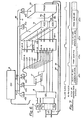
- this embodiment is comprised of a control section, which is illustrated in the top portion of Figure 1; and a data section, which is illustrated in the bottom portion of that figure.
- the function of the control section is to sequentially generate control words, while the function of the data section is to simultaneously transform operands in response to those control words.
- control section includes a set of N memories 10-1, 10-2, ... 10-N arranged in a bit-sliced fashion.
- Each of these N memories have first address inputs Al-A3, second address inputs A4-A6, and a pair of outputs Ql-Q2.
- signals on the outputs Q1 and Q2 from all of those N memories are summed by an adder 11, and the result is held in a register 12.
- the least significant bit position of register 12 is fed back to one of the three first address inputs, namely, A3 of memory 10-1; the next bit position in order of significance of register 12 is fed back to the first address input A3 of memory 10-2, and so on.
- Register 12 has as many bit positions as there are memories in the set of N memories. As will be seen, the function of register 12 is to store the address of the current control word.
- All of the bits of register 12 also couple via bus 13 to a link register 14.
- Bus 13 is a N-bit bus and register 14 is at least N-bits wide.
- the least significant bit position of the link register 14 connects to another one of the three first address inputs, namely, A2 of memory 10-1, while the next bit position of link register 14 in order of significance connects to the first address input A2 of memory 10-2, and so on.
- control memory 15 Associated with the N memory set 10 is a control memory 15. Address information for the control memory 15 is obtained from register 12, which has its outputs connected to the address inputs of control memory 15. This control memory 15 contains a plurality of control words which are read onto a bus 16. One portion 16a of the bus 16 is fed back to the second address inputs A4-A6 of all of the N memories, 10-1 through 10-N; while another portion 16b of the bus 16 is connected to the address inputs B1-B4 of a memory 17. Address inputs B5-B12 of that memory are selectively coupled to the output of one of a plurality of registers R1, R2, ... RN through a selector 19. The outputs 18 of the memory 17 is coupled respectively to one of the three first address inputs, namely, A1 of each of the N memories 10-1 through 10-N.
- All of the above components 10 through 19 of the control section operate to sequentially generate control words with a minimum of hardwired logic.
- register 12 is reset to some predetermined address, such as all 0's.
- the control word stored in the control memory 15 at that address is then read out onto bus 16.
- memory 17 is designed to provide on its outputs 18, a transformation of the bits on its inputs B5-B 12, which bits are obtained from the information stored in the plurality of register R1-RN.
- each of the N memories 10-1 through 10-N is designed to provide on their respective outputs, Q1 and Q2, a transformation of the information bits on their three first address inputs, A1-A3.
- Adder 11 in turn sums the signals on outputs Q1 and Q2 from all of the N memories, and the result constitutes the address of the next control word to be obtained from control memory 15.
- the function of the set of N-memories 10 and the memory 17 is essentially to perform a transformation of the information utilized to address these memories. This function is achieved by employing a novel structure and technique requiring a minimum of logic. To illustrate the versatility and flexibility which can be achieved, reference is made to Figure 2 and the following discussion.
- control section In the example of row 1 of Figure 2, the control section generates the next address for the control memory 15 such that it equals the present address PA in the register 12 plus either a number N1 or N2 depending upon whether or not bit 1 of the appropriate register R1 through RN selected by selector 19 equals a 1.
- the memory 17 is made responsive to a predetermined code (such as 0) on its address inputs B1-B4 to provide at its output 18 the constant N or N2, depending upon whether or not bit 1 of the signals on its address inputs B5-B 12 is a 1.
- signals for B1-B4 are provided by the output of control memory 15, while B5-B12 are provided by the output of the selector 19.
- the N-memories 10-1 through 10-N are made responsive to a predetermined code (such as 0) on their second address inputs A4-A6 to provide signals on their outputs Q1 and Q2, respectively, indicating the sum and carry that is produced by adding the bits on their first address inputs from register 12 and memory 17.
- memories 10-1 through 10-N appear to act both as a selector and an adder of the bits on their A1 and A3 inputs. Each memory has two outputs in order that sum and carry signals can be simultaneously produced. Adder 11 then completes the arithmetic process by enabling the carries to propagate from bit to bit.
- memory 17 is made responsive to a predetermined code on its address inputs B1-B4 (such as a code of 1) to provide the constant N on its outputs 18 when bit 2 of the selected register applied to the address inputs B5- ⁇ 12 of memory 17 equals 1, and to provide the constant N2 when that bit equals 0.
- a code of 1 is then achieved by applying a code of 1 to the address inputs B1-84 of memory 17 and simultaneously applying the previously described code of 0 to the address inputs A4-A6 of memories 10-1 through 10-N.
- next address is made equal to the present address plus either constants N1, N2, N3, or N4 depending upon whether bits 1 and 2 of the selected register equal 00, 01, 10, or 11, respectively.
- memory 17 is made responsive to another code on its address inputs B1-B4 (such as a code of 2) to provide on its outputs 18, the constants N 1, N2, N3, or N4 depending upon the state of bits 1 and 2 applied to its address inputs B5-B12.
- the desired function is then achieved by applying a code of 2 to the address inputs B1-B4 of the memory 17 and simultaneously applying the previously described code of 0 to the address inputs A4-A6 of the memories 10-1 through 10-N.
- memories 10-1 through 10-N are made responsive to a new predetermined code on their address inputs A4-A6 (such as a code of 1) to provide signals on their outputs indicating the sum and carry that is obtained by adding the bits on their address input A1 and A3 to the constant C.
- the memories 10-1 through 10-N appear to simultaneously perform the functions of selecting bits on their address inputs A1 and A3, obtaining the constant C, and adding the selected bits to that constant.
- the control word address is formed by adding a predetermined constant to the contents of the link register 14.
- This is achieved by making memories 10-1 through 10-N responsive to another code on their address inputs A4-A6 (such as a code of 2), which is portion 16a of a control word from control memory 15, to provide on their respective outputs Q1 and Q2 the sum and carry that are obtained by adding the corresponding bits of the contents of the link register 14 to the constant.
- the memories 10-1 through 10-N appears to perform the function of selecting the contents of the link register 14, obtaining the constant C, and adding the corresponding bits of those two entities.
- control section operates to modify the contents of the link register 14 by an amount of either N1 or N2 depending upon whether bit 2 of the selector register R1-RN is equal to 1 or 0. This is accomplished by applying the previously described code of 1 to the address inputs B1-B4 of memory 17; and by simultaneously making the memories 10-1 through 10-N responsive to a new code on their address inputs A4-A6 (such as a code of 3) to provide on their outputs, signals representing the sum and carry of the bits on their respective A1 and A2 address inputs.
- the control word address is formed by combining some of the bits of register 12 with other bits from the output of memory 17.
- the particular example illustrated combines bits 7-N of the contents of register 12 with bits 1-6 from the output of memory 17. This is achieved by making memories 10-1 through 10-6 responsive to a predetermined code (such as 4) on their address inputs A4-A6 to provide signals on their respective outputs equal to the signals on their A1 address inputs; and by making memories 10-7 through 10-N responsive to that same code to provide signals on their outputs equal to the signals on their A3 to address inputs.
- a predetermined code such as 4
- memories 10-1 through 10-N are to respond by providing signals representing the sum and carry that is obtained by adding corresponding bits of the present address and the output of memory 17.
- the present address of regiser 12 is received on address inputs A3, and the output of memory 17 is received on address inputs A1.
- the Q1 output column indicates the sum of address inputs A1 and A3; and the Q2 output column indicates the corresponding carry.
- memories 10-1 through 10-N respond by providing output signals representing the sum and carry that is obtained by adding corresponding bits of the present address, the output from memory 17, and a predetermined constant C. Any particular bit of that constant could be a "1" " or a "0".
- outputs Q1 and Q2 of the right most column respectively indicate the sum and carry that are obtained by adding a "1” to the bits on address inputs A1 and A3.
- outputs Q1 and Q2 of the adjacent column respectively indicate the sum and carry that are obtained by adding a "0" to those same address bits.
- memories of 10-1 through 10-N provide signals indicating the sum and carry obtained by adding a constant C to the contents of the link register 14. Those memories where the bit of constant C equals 1 have outputs Q1 and Q2 as illustrated in the right most column; and the remaining memories have outputs as illustrated in the adjacent column.
- one portion of the memories 10-1 through 10-N must respond by passing the signals from the output of register 12, while the remaining memories are to pass signals from bus 18.
- the remaining memories 10-7 through 10-N are arranged to provide a 01 as output signals indicating the state of the bits on their A3 address inputs, as is illustrated in the next adjacent column.
- each of the memories 30-1 through 30-N have first address inputs C1-C4, second address inputs C5-C8, and two pairs of outputs D1-D2 and D3-D4.
- the function of the memories 30-1 through 30-N is to respond to various codes on their second address inputs C5-C8 by providing signals on their outputs representing selectable transformations of the signals on their first address inputs Cl-C4.
- Outputs D1 and D2 of all of the memories are coupled to a first adder 31, and outputs D3-D4 of all of the memories are coupled to another adder 32. These adders in turn have their respective outputs 31A and 32A coupled to a programmable multiplexer 33.
- the multiplexer 33 operates to select and shift the signals from the adders 31 and 32 onto a pair of output buses 34 and 35, which in turn feed back to registers R1-RN.
- All of these components of the data section operate to transform operands in response to the control words as follows. Initially, various portions of the control word from the control memory 15 are placed into a plurality of registers 36A, 36B, 36C, and 36D. The selector 19 then responds to the portion of the control word in register 36A by passing the contents of four of the registers R 1-RN to the first address inputs C1-C4 of memories 30-1 through 30-N. Memory 30-1 receives the least significant bits on its C1-C4 inputs; memory 30-2 receives the next bit in order of significance on its C1-C4 inputs; etc.
- that portion of the control word which is in register 36B is bused in parallel to the second address inputs C5-C8 of all of the memories 30-1 through 30-N.
- the memories are responsive to that portion of the control word to select various bits on their first address inputs C1-C4, to internally obtain constants, and to provide signals on their outputs representing transformations of those selected inputs and constants.
- Row 1 contains a mathematical expression which indicates that, in general, outputs Dl-D2 represent one selectable transformation T1 of an arbitrary number N1 and the bits on the address inputs C1-C4; and outputs D3-D4 represent another totally independent transformation T2. Specific examples of this general case are expressed in rows 2 and 3.
- the signals appearing at the outputs D1 and D2, respectively, represent the sum and carry of the bits on address inputs C1 and C2 to the memories; and the signals appearing at the outputs D3 and D4, respectively, represent the sum and carry of the bits on address inputs C3 and C4 to the memories.
- This transformation is useful in performing double word arithmetic.
- the signals at outputs D1 and D2 represent the result of logically ANDing bits on address input C1 and C2, ORing the result with the bit on address C3, ORing that result with the inverse of the bits on address input C4, and ANDing that result with an arbitrary mask M.
- T1 and T2 illustrates the generality of the transformation T1 and T2.
- the signals appearing at outputs D3 and D4 could independently represent signals indicating the sum and carry obtained by adding or subtracting bits on any of the address inputs C1-C4 to the memories and an arbitrary constant N3.
- FIG. 5 there is shown a timing diagram that illustrates the manner in which the above described control and data sections interact.
- the control section uses the address in register 12 to fetch a control word (CW#1) from control memory 15.
- the control section forms the address of the next control word by the transformation action of memories 10-1 through 10-N and memory 17. This fetching of CW#1 and address formation is complete at the end of time interval ⁇ t1.
- control word CW#1 is implemented and directs the operation of the data section. This includes directing the transformation which memories 30-1 through 30-N to perform, directing the selecting and shifting which the programmable multiplexer 33 performs, etc. Also during time interval At2, the control section simultaneously forms the address of the next control word (CW#3). These simultaneous operations of transforming operands in the data section and calculating subsequent addresses in the control section is repeated during each of the time intervals At3, At4 ... which follow.
- FIG. 6 illustrates another embodiment of the invention.
- the data section and control section are combined into one composite or integrated unit.
- This integrated unit includes some of the components as previously described in the control and data sections of Figure 1.
- Also included in this second embodiment is a plurality of 2x 1 multiplexers 40A-40E. These multiplexers operate to pass one portion of the presently active control word retrieved from control memory 15 during spaced apart time intervals, and pass the remaining portion of the retrieved control words during the period between those spaced apart time intervals. This enables the integrated control-data section to alternately operate on data and form the address for the next control word. This sequential operation is illustrated in the timing diagram of Figure 7.
- various operands in registers R1 ... Rn are selectively transformed during the spaced apart time intervals ⁇ t11, ⁇ t13, etc.; and the address of the next control word is formed during time intervals ⁇ t12, ⁇ t14, etc. Transformation of the data is accomplished in response to that portion of the control word on a bus 41. Similarly, formation of the address of the next control word is accomplished in response to that portion of the present control word on bus 42. This portion is passed through the 2x 1 multiplexers 40A--40E during time intervals ⁇ t12, ⁇ t14, ... etc.
- Figure 6 embodiment requires a minimal amount of memory for its physical implementation. This is due to the fact that the memories 30-1 through 30-N of Figure 1 are time shared to alternately transform data in registers R1-RN and form addresses for the control words stored in the control memory 15. In comparison, an advantage of the Figure 1 embodiment is that it performs the address transformations and the data transformations simultaneously. This simultaneity, however, is achieved at the expense of incorporating additional hardware-i.e., memories 10-1 through 10-N and the adder 11. Thus, the two embodiments offer a trade off between performance and space.
- bit 1 the least significant bit (bit 1) of all of the registers R1-RN and the corresponding portion of the selector 19 are indicated by reference numeral 50-1.
- reference numerals 50-2, ... 50-N-1, 50-N respectively indicate bit 2, bit N-1, and bit N of all of the registers and their corresponding selector portion.
- a plurality of leads 51 run between those registers as illustrated. One lead is provided for each register; and a signal is applied to the lead to select the corresponding register. Bit 1 of the selected register is gated onto leads 52-1; bit N of the selected register is gated onto leads 52-N; etc.
- Memory 30-1 lies alongside of registers 50-1; and its Cl-C4 address inputs are respectively coupled to the leads 52-1.
- memory 30-N lies alongside of registers 50-N; and its C1-C4 address inputs are respectively coupled to leads 52-N.
- a bus 53 of leads runs alongside of memories 30-1 through 30-N. This bus couples in parallel the address inputs C5-C8 of all of the memories; and it carries decode signals of the presently active control word for these memories.
- Adder 31 runs alongside of bus 53 as illustrated. It receives the D1 and D2 output signals from all of the memories 30-1 through 30-N. Similarly, adder 32 runs alongside of adder 31; and it receives the D3 and D4 output signals from all of the memories.
- Multiplexer 33 lies between the adders 31 and 32; and it receives control signals from the control word on leads 54. Outputs from the multiplexer are coupled back to registers 50-1 through 50-N by leads 55-1 through 55-N, respectively.
- multiplexer 33 includes two sets of N metal lines 60-1 through 60-2N. Half of them (lines 60-1 through 60-N) carry output signals from adder 31; whereas the other half carry output signals from adder 32.
- Lying between lines 60-N and 60-N+1 is another set of metal lines 54. They carry control signals which are decodes of that portion of the control word that is sent to the multiplexer. One line is provided for each function that the multiplexer performs.
- Each of the metal lines 54 connect via respective polysilicon leads 61 to transistor 62 and 63 as illustrated.
- the source of the transistors 62 are all connected to one of the multiplexer's output lines 55-1; and the source of the transistors 63 are connected to one of the output lines 55-N.
- each of the transistors 62 and 63 have a drain which is respectively connected to the diffusions 64 and 65. These diffusions run beneath and perpendicular to all of the metal lines 60-1 through 60-2N.
- each of the diffusions 64 are selectively connected to one of the overlying metal lines during the fabrication process. Reference numerals 66 and 67 illustrate examples of where these contacts could be made.
- each of the diffusions 65 is selectively connected to one of the metal lines 60-1 through 60-2N. Examples of these connections are indicated by reference numerals 68 and 69.
- FIG. 9b there is illustrated a portion of one of the memories 30-1 through 30-N. It includes a plurality of spaced apart metal lines 80-1, 80-2, ... as illustrated. One metal line is provided for each possible code on the memories second address inputs C5-C8. These metal lines are coupled through respective transistors 81-1,--$1-2, ... to one of the memories outputs, such as output D1. Transistors 81-1, 81-2, ... are selectively enabled by a decode of the second address inputs C5-C8.
- a plurality of polysilicon lines 82-1, 82-2,... lie under and run perpendicular to the metal lines. Signals SS1, SS2, ... are selectively generated on one of the polysilicon lines 82-1, 81-2, ... by a decoder of the C1-C4 address inputs.
- Polysilicon line 82-1 forms the gate of a plurality of transistors T1, T2, ... Ti whose sources and drains are formed by a diffusion 83-1.
- polysilicon line 82-2 forms the gates of a plurality of transistors T1, T2, ... Ti whose sources and drains are formed by a diffusion 83-2.
- Reference numerals 84 indicate one exemplary set of contacts between the diffusions 83 and the metal lines 80. The absence of a contact is indicated by reference numerals 85.
- the D1 output signals may be made either a logical 0 or a logical 1 in accordance with the previously described Figure 3 by including or excluding the appropriate contact 84.
- All of the optional contacts in the Figure 9b memories are made in the same manner as the optional contacts in the Figure 9a programmable multiplexer. That is, the optional contacts in both of those components are made between a metal line and a diffusion. Thus, the entire operation of the disclosed embodiments can be changed completely simply by reworking the mask that defines the location of the holes for those contacts.
- the optional connections in the Figure 9a programmable multiplexer, and the optional contacts in the Figure 9b memory may be made at the diffusion level. That is in Figure 9a, the metal to diffusion connections in holes 66, 67, 68, and 69 would always be made; and in Figure 9b, the metal to diffusion connections in holes 84 and 85 would also always be made. Then a small (e.g. 3-4 micros) patch would optionally be provided in the diffusions near the above connections.
- memories 10-1 through 10-N could be read/write or PROM type memories.
- memories 30-1 through 30-N of either the Figure 1 or Figure 6 embodiment could be similarly modified.
- any of the registers R1-RN, Link, and PA may be content addressable, or part of a stack. Therefore, since many such modifications are possible, it is to be understood that the invention is not limited to said details but as defined by the appended claims.
Description
- This invention relates to digital computers; and more particularly to the computer's overall architecture. In the prior art, a wide variety of computer architectures existed. However, they all basically fall into the two broad categories of being either a microprogrammed or a non-microprogrammed machine.
- A non-microprogrammed computer can be characterized as one which interprets and executes user level instructions directly with a plurality of hardwired logic gates. In comparison, a microprogrammed computer interprets and executes each user level instruction by executing a series of microcommands. These microcommands in turn are interpreted and executed by the hardwired logic gates.
- One attractive feature of the microprogrammed computer is its regularity and simplicity in architecture. This is due to the fact that the microcommands, which the hardwired logic interprets and executes, generally are much simpler than the corresponding user level commands. Thus, a microprogrammed computer having one particular user level command set generally will contain substantially fewer hardware logic gates than a non-microprogrammed computer with the same user level command set.
- Those logic gates which are eliminated in the microprogrammed computer however, are replaced with a set of microcommands in the control memory. Thus, the total hardware in a microprogrammed computer, including the control memory, is generally about the same as that in a corresponding non-microprogrammed computer. However, it is much easier to modify microcommands in a control memory than it is to add and delete hardwired logic gates and their interconnections. This is a most important requirement in computers whose user level language is subject to change, and in computers, which emulate several user level languages. Thus, another feature of a microprogrammed computer, and perhaps its most important feature is its flexibility and the ease with which modifications can be incorporated.
- But in the prior art, the extent to which even a microprogrammed computer could be modified was constrained because the logic which implemented the microcommands was hardwired. Thus, the set of microcommands that a programmer could use was fixed; and only their order in the control memory was programmable. Accordingly, new types of microcommands could be added only at the expense of modifying various hardwired logic gates and their interconnections. And this made the personality of the machine too rigid.
- However, in an article by D. Wyland, published in
Electronics Volume 51, No. 10, a memory organisation is described, including a control memory for storing control words, addressed by outputs from a PROM, itself addressed partly by op-codes from the micro instruction register and partly by operands from instruction registers. - Further, German Offenlegungsschrift 2418941 discloses a memory organisation of 3 ROMs, each handling a 2-bit slice addressed by operands and op-codes. At each addressable memory location there is stored a signal which represents a transformation of the operand portion of the address of that location, which transformation is specified by the op-code portion of said address.
- The object of this invention is to provide a more flexible architecture for a digital computer.
- In accordance with the present invention, the control section of a digital computer includes a plurality of registers, each having its ith bit coupled to a first address input on the ith one of N memories, where i=1, ...N. The second address inputs of the N memories are coupled to a control memory to receive a portion of the presently active memory control word therefrom. Each of the N memories is responsive to the control word portion on its second address inputs to generate signals on its pair of outputs, representing programmable arithmetic transformations of the bits on its first address inputs. The signals on the pairs of outputs of all the N memories are combined and fed to the control memory to address a successive control word. Preferably the N memories are programmable. This allows the types of branches which are taken to be readily modified. It is to be understood that the exact type of transformation which occurs in response to any particular control word portion is programmable.
- A similar programmable structure can be employed in the data section of the computer. This programmable structure includes a set of N memories where each of the N memories has first address inputs, two pairs of outputs, and second address inputs which are coupled to the control section to receive a portion of a presently active control word. Each memory of the set is responsive to the control word portion on its second address inputs to provide transformations of the information bits on their first address inputs. These information bits are provided by a plurality of N-bit wide registers which have their ith bit coupled to a first address input on the ith one of the N memories, where i=1, ...N. The respective pairs of outputs for each of the N-memories are provided as inputs to a pair of adders, the outputs of which being coupled as inputs to a programmable multiplexer. The multiplexer shifts the output of the adder by a programmable number of bit positions in response to another portion of the active control word.
- In another embodiment of the invention, the control and data section are integrated and share a single memory organization. In this embodiment, control words are generated during spaced apart time intervals, while operands are transformed in response to those control words between the spaced apart time interval. This programmable structure also includes a set of N memories arranged in a bit-sliced fashion, each of the N memories have first address inputs, second address inputs, and two pairs of outputs. Associated with the memory organization is a plurality of N-bit wide registers, which have their ith bit coupled to a first address input of the ith one of the N memories, where i=1, ...N. In addition, there are first and second adder means, respectively, coupled to the output pairs of the N memories. A control memory has address signals coupled to receive an address from one of the plurality of registers, and has outputs for forming the control words thereon. A plurality of 2xl switches couple one portion of the control words to the second address inputs of all of the N memories during the spaced apart time intervals, and couple another portion of the control words thereto between the spaced time intervals.
- Various features and advantages of the inventions will best be understood by reference to the following detailed description and accompanying drawings wherein:
- Figure 1 is a schematic block diagram of a digital computer constructed according to the invention.
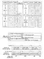
- Figure 2 illustrates various transformations that are performed by the set of N memories in the control section of the Figure 1 embodiment.
- Figure 3 illustrates one suitable code for the set of N memories which achieves the transformations of Figure 2.
- Figure 4 illustrates representative examples of the transformations that are performed by the set of N memories in the data section of the Figure 1 embodiment.
- Figure 5 is a timing diagram illustrating the sequence by which the data section and control section of the Figure 1 embodiment interact.
- Figure 6 is a schematic block diagram illustrating another embodiment of the invention.
- Figure 7 is a timing diagram illustrating the sequential operation of the Figure 6 embodiment.
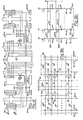
- Figure 8 is a greatly enlarged plan view of a physical layout on a semiconductor chip for a portion of the Figure 1 and Figure 6 embodiments.
- Figure 9a is a detailed circuit diagram and physical layout for the programmable multiplexer of Figure 8.
- Figure 9b is a detailed circuit diagram and physical layout for one memory of the set in the physical layout of Figure 8.
- Referring now to Figure 1, a preferred embodiment of the invention will be described. Basically, this embodiment is comprised of a control section, which is illustrated in the top portion of Figure 1; and a data section, which is illustrated in the bottom portion of that figure. The function of the control section is to sequentially generate control words, while the function of the data section is to simultaneously transform operands in response to those control words.
- Included in the control section is a set of N memories 10-1, 10-2, ... 10-N arranged in a bit-sliced fashion. Each of these N memories have first address inputs Al-A3, second address inputs A4-A6, and a pair of outputs Ql-Q2. In operation, signals on the outputs Q1 and Q2 from all of those N memories are summed by an
adder 11, and the result is held in aregister 12. Then, the least significant bit position ofregister 12 is fed back to one of the three first address inputs, namely, A3 of memory 10-1; the next bit position in order of significance ofregister 12 is fed back to the first address input A3 of memory 10-2, and so on. Register 12 has as many bit positions as there are memories in the set of N memories. As will be seen, the function ofregister 12 is to store the address of the current control word. - All of the bits of
register 12 also couple via bus 13 to alink register 14. Bus 13 is a N-bit bus andregister 14 is at least N-bits wide. The least significant bit position of thelink register 14 connects to another one of the three first address inputs, namely, A2 of memory 10-1, while the next bit position oflink register 14 in order of significance connects to the first address input A2 of memory 10-2, and so on. - Associated with the N memory set 10 is a
control memory 15. Address information for thecontrol memory 15 is obtained fromregister 12, which has its outputs connected to the address inputs ofcontrol memory 15. Thiscontrol memory 15 contains a plurality of control words which are read onto abus 16. One portion 16a of thebus 16 is fed back to the second address inputs A4-A6 of all of the N memories, 10-1 through 10-N; while anotherportion 16b of thebus 16 is connected to the address inputs B1-B4 of amemory 17. Address inputs B5-B12 of that memory are selectively coupled to the output of one of a plurality of registers R1, R2, ... RN through aselector 19. Theoutputs 18 of thememory 17 is coupled respectively to one of the three first address inputs, namely, A1 of each of the N memories 10-1 through 10-N. - All of the
above components 10 through 19 of the control section operate to sequentially generate control words with a minimum of hardwired logic. Initially, register 12 is reset to some predetermined address, such as all 0's. The control word stored in thecontrol memory 15 at that address is then read out ontobus 16. In response to theportion 16b of the control word,memory 17 is designed to provide on itsoutputs 18, a transformation of the bits on its inputs B5-B 12, which bits are obtained from the information stored in the plurality of register R1-RN. In response to the presence of portion 16a of a retrieved control word, each of the N memories 10-1 through 10-N is designed to provide on their respective outputs, Q1 and Q2, a transformation of the information bits on their three first address inputs, A1-A3.Adder 11 in turn sums the signals on outputs Q1 and Q2 from all of the N memories, and the result constitutes the address of the next control word to be obtained fromcontrol memory 15. - The function of the set of N-
memories 10 and thememory 17 is essentially to perform a transformation of the information utilized to address these memories. This function is achieved by employing a novel structure and technique requiring a minimum of logic. To illustrate the versatility and flexibility which can be achieved, reference is made to Figure 2 and the following discussion. - In the example of
row 1 of Figure 2, the control section generates the next address for thecontrol memory 15 such that it equals the present address PA in theregister 12 plus either a number N1 or N2 depending upon whether or notbit 1 of the appropriate register R1 through RN selected byselector 19 equals a 1. - To accomplish this, the
memory 17 is made responsive to a predetermined code (such as 0) on its address inputs B1-B4 to provide at itsoutput 18 the constant N or N2, depending upon whether or notbit 1 of the signals on its address inputs B5-B 12 is a 1. Remember that signals for B1-B4 are provided by the output ofcontrol memory 15, while B5-B12 are provided by the output of theselector 19. At the same time, the N-memories 10-1 through 10-N are made responsive to a predetermined code (such as 0) on their second address inputs A4-A6 to provide signals on their outputs Q1 and Q2, respectively, indicating the sum and carry that is produced by adding the bits on their first address inputs fromregister 12 andmemory 17. - In performing this transformation, memories 10-1 through 10-N appear to act both as a selector and an adder of the bits on their A1 and A3 inputs. Each memory has two outputs in order that sum and carry signals can be simultaneously produced.
Adder 11 then completes the arithmetic process by enabling the carries to propagate from bit to bit. - Consider next the address transformation indicated in
row 2 of Figure 2. That transformation is similar to the transformation described forrow 1, with the only exception being thatbit 2 rather thanbit 1 of the selected register R1-RN is tested. To accomplish this function,memory 17 is made responsive to a predetermined code on its address inputs B1-B4 (such as a code of 1) to provide the constant N on itsoutputs 18 whenbit 2 of the selected register applied to the address inputs B5-θ12 ofmemory 17 equals 1, and to provide the constant N2 when that bit equals 0. The desired address transformation is then achieved by applying a code of 1 to the address inputs B1-84 ofmemory 17 and simultaneously applying the previously described code of 0 to the address inputs A4-A6 of memories 10-1 through 10-N. - Next, in
row 3 of Figure 2, an example of a four-way branch is illustrated. There, the next address is made equal to the present address plus either constants N1, N2, N3, or N4 depending upon whetherbits memory 17 is made responsive to another code on its address inputs B1-B4 (such as a code of 2) to provide on itsoutputs 18, theconstants N 1, N2, N3, or N4 depending upon the state ofbits memory 17 and simultaneously applying the previously described code of 0 to the address inputs A4-A6 of the memories 10-1 through 10-N. - A modification of this four-way branch is illustrated in
row 4 of Figure 2. There, the tests which are performed on the selected register remain the same, but the increment by which the present address is modified changes by a constant C. To accomplish this function, memories 10-1 through 10-N are made responsive to a new predetermined code on their address inputs A4-A6 (such as a code of 1) to provide signals on their outputs indicating the sum and carry that is obtained by adding the bits on their address input A1 and A3 to the constant C. In this case, the memories 10-1 through 10-N appear to simultaneously perform the functions of selecting bits on their address inputs A1 and A3, obtaining the constant C, and adding the selected bits to that constant. - Next, in the example of
row 5, the control word address is formed by adding a predetermined constant to the contents of thelink register 14. This is achieved by making memories 10-1 through 10-N responsive to another code on their address inputs A4-A6 (such as a code of 2), which is portion 16a of a control word fromcontrol memory 15, to provide on their respective outputs Q1 and Q2 the sum and carry that are obtained by adding the corresponding bits of the contents of thelink register 14 to the constant. In this case, the memories 10-1 through 10-N appears to perform the function of selecting the contents of thelink register 14, obtaining the constant C, and adding the corresponding bits of those two entities. - In
row 6 of Figure 2, the control section operates to modify the contents of thelink register 14 by an amount of either N1 or N2 depending upon whetherbit 2 of the selector register R1-RN is equal to 1 or 0. This is accomplished by applying the previously described code of 1 to the address inputs B1-B4 ofmemory 17; and by simultaneously making the memories 10-1 through 10-N responsive to a new code on their address inputs A4-A6 (such as a code of 3) to provide on their outputs, signals representing the sum and carry of the bits on their respective A1 and A2 address inputs. - Next, in the example of
row 7 of Figure 2, the control word address is formed by combining some of the bits ofregister 12 with other bits from the output ofmemory 17. The particular example illustrated combines bits 7-N of the contents ofregister 12 with bits 1-6 from the output ofmemory 17. This is achieved by making memories 10-1 through 10-6 responsive to a predetermined code (such as 4) on their address inputs A4-A6 to provide signals on their respective outputs equal to the signals on their A1 address inputs; and by making memories 10-7 through 10-N responsive to that same code to provide signals on their outputs equal to the signals on their A3 to address inputs. - Referring now to Figure 3, the coding for memories 10-1 through 10-N which achieves the above functions will be described. In that figure, the symbols A1 through A6 correspond to address inputs Al-A6 on any of the memories 10-1 through 10-N.
- When the A6-A4 address inputs receive a control word of 000, memories 10-1 through 10-N are to respond by providing signals representing the sum and carry that is obtained by adding corresponding bits of the present address and the output of
memory 17. The present address ofregiser 12 is received on address inputs A3, and the output ofmemory 17 is received on address inputs A1. Thus, where A6-A4 equals 000 as shown in Figure 3, the Q1 output column indicates the sum of address inputs A1 and A3; and the Q2 output column indicates the corresponding carry. - Similarly, when address inputs A6-A4 receive a control word of 001, memories 10-1 through 10-N respond by providing output signals representing the sum and carry that is obtained by adding corresponding bits of the present address, the output from
memory 17, and a predetermined constant C. Any particular bit of that constant could be a "1" " or a "0". In Figure 3, outputs Q1 and Q2 of the right most column respectively indicate the sum and carry that are obtained by adding a "1" to the bits on address inputs A1 and A3. And outputs Q1 and Q2 of the adjacent column respectively indicate the sum and carry that are obtained by adding a "0" to those same address bits. - Next, in response to a code of 010 on address inputs A6-A4, memories of 10-1 through 10-N provide signals indicating the sum and carry obtained by adding a constant C to the contents of the
link register 14. Those memories where the bit of constant C equals 1 have outputs Q1 and Q2 as illustrated in the right most column; and the remaining memories have outputs as illustrated in the adjacent column. - Finally, in response to a code of 100, one portion of the memories 10-1 through 10-N must respond by passing the signals from the output of
register 12, while the remaining memories are to pass signals frombus 18. To achieve this, the first six memories 10-1 through 10-6 are arranged to provide a 01 as output signals indicating the state of their A1 address input. This is indicated in the right most column where any word addressed with A1=1 has a "1" as its content, and any word addressed with A1=0 has a "0" as its contents. The remaining memories 10-7 through 10-N are arranged to provide a 01 as output signals indicating the state of the bits on their A3 address inputs, as is illustrated in the next adjacent column. - Referring now back to Figure 1, the structure and operation of that computer's data section will be described. It includes a set of N memories 30-1, 30-2, ... 30-N, which is quite similar to the control section. Each of the memories 30-1 through 30-N have first address inputs C1-C4, second address inputs C5-C8, and two pairs of outputs D1-D2 and D3-D4. Basically, the function of the memories 30-1 through 30-N is to respond to various codes on their second address inputs C5-C8 by providing signals on their outputs representing selectable transformations of the signals on their first address inputs Cl-C4.
- Outputs D1 and D2 of all of the memories are coupled to a
first adder 31, and outputs D3-D4 of all of the memories are coupled to anotheradder 32. These adders in turn have their respective outputs 31A and 32A coupled to aprogrammable multiplexer 33. Themultiplexer 33 operates to select and shift the signals from theadders output buses - All of these components of the data section, operate to transform operands in response to the control words as follows. Initially, various portions of the control word from the
control memory 15 are placed into a plurality of registers 36A, 36B, 36C, and 36D. Theselector 19 then responds to the portion of the control word in register 36A by passing the contents of four of the registers R 1-RN to the first address inputs C1-C4 of memories 30-1 through 30-N. Memory 30-1 receives the least significant bits on its C1-C4 inputs; memory 30-2 receives the next bit in order of significance on its C1-C4 inputs; etc. - At the same time, that portion of the control word which is in register 36B is bused in parallel to the second address inputs C5-C8 of all of the memories 30-1 through 30-N. In turn, the memories are responsive to that portion of the control word to select various bits on their first address inputs C1-C4, to internally obtain constants, and to provide signals on their outputs representing transformations of those selected inputs and constants.
- Some representative transformations which memories 30-1 through 30-N perform are illustrated in Figure 4.
Row 1 contains a mathematical expression which indicates that, in general, outputs Dl-D2 represent one selectable transformation T1 of an arbitrary number N1 and the bits on the address inputs C1-C4; and outputs D3-D4 represent another totally independent transformation T2. Specific examples of this general case are expressed inrows - In
row 2, the signals appearing at the outputs D1 and D2, respectively, represent the sum and carry of the bits on address inputs C1 and C2 to the memories; and the signals appearing at the outputs D3 and D4, respectively, represent the sum and carry of the bits on address inputs C3 and C4 to the memories. This transformation is useful in performing double word arithmetic. Next, in the example ofrow 3, the signals at outputs D1 and D2 represent the result of logically ANDing bits on address input C1 and C2, ORing the result with the bit on address C3, ORing that result with the inverse of the bits on address input C4, and ANDing that result with an arbitrary mask M. This illustrates the generality of the transformation T1 and T2. At the same time, the signals appearing at outputs D3 and D4 could independently represent signals indicating the sum and carry obtained by adding or subtracting bits on any of the address inputs C1-C4 to the memories and an arbitrary constant N3. - Next, referring to Figure 5, there is shown a timing diagram that illustrates the manner in which the above described control and data sections interact. During a time interval Δt1, the control section uses the address in
register 12 to fetch a control word (CW#1) fromcontrol memory 15. At the same time, the control section forms the address of the next control word by the transformation action of memories 10-1 through 10-N andmemory 17. This fetching ofCW# 1 and address formation is complete at the end of time interval Δt1. - Subsequently, during time interval At2, control
word CW# 1 is implemented and directs the operation of the data section. This includes directing the transformation which memories 30-1 through 30-N to perform, directing the selecting and shifting which theprogrammable multiplexer 33 performs, etc. Also during time interval At2, the control section simultaneously forms the address of the next control word (CW#3). These simultaneous operations of transforming operands in the data section and calculating subsequent addresses in the control section is repeated during each of the time intervals At3, At4 ... which follow. - Reference now is made to Figure 6, which illustrates another embodiment of the invention. In this embodiment, the data section and control section are combined into one composite or integrated unit. This integrated unit includes some of the components as previously described in the control and data sections of Figure 1.
- In particular, it includes the
present address register 12,link register 14,control memory 15, andmemory 17 of the Figure 1 control section. And it includes memories 30-1 through 30-N,adders programmable multiplexer 33, and registers R1-RN of the Figure 1 data section. These components are interconnected as illustrated in Figure 6. - Also included in this second embodiment is a plurality of
2x 1 multiplexers 40A-40E. These multiplexers operate to pass one portion of the presently active control word retrieved fromcontrol memory 15 during spaced apart time intervals, and pass the remaining portion of the retrieved control words during the period between those spaced apart time intervals. This enables the integrated control-data section to alternately operate on data and form the address for the next control word. This sequential operation is illustrated in the timing diagram of Figure 7. - In that figure, various operands in registers R1 ... Rn are selectively transformed during the spaced apart time intervals Δt11, Δt13, etc.; and the address of the next control word is formed during time intervals Δt12, Δt14, etc. Transformation of the data is accomplished in response to that portion of the control word on a
bus 41. Similarly, formation of the address of the next control word is accomplished in response to that portion of the present control word onbus 42. This portion is passed through the2x 1 multiplexers 40A--40E during time intervals Δt12, Δt14, ... etc. - One attractive feature of the Figure 6 embodiment is that it requires a minimal amount of memory for its physical implementation. This is due to the fact that the memories 30-1 through 30-N of Figure 1 are time shared to alternately transform data in registers R1-RN and form addresses for the control words stored in the
control memory 15. In comparison, an advantage of the Figure 1 embodiment is that it performs the address transformations and the data transformations simultaneously. This simultaneity, however, is achieved at the expense of incorporating additional hardware-i.e., memories 10-1 through 10-N and theadder 11. Thus, the two embodiments offer a trade off between performance and space. - Next, referring to Figure 8, one physical layout for the invention on a semiconductor chip will be described. In this layout the least significant bit (bit 1) of all of the registers R1-RN and the corresponding portion of the
selector 19 are indicated by reference numeral 50-1. Similarly, reference numerals 50-2, ... 50-N-1, 50-N respectively indicatebit 2, bit N-1, and bit N of all of the registers and their corresponding selector portion. - A plurality of
leads 51 run between those registers as illustrated. One lead is provided for each register; and a signal is applied to the lead to select the corresponding register.Bit 1 of the selected register is gated onto leads 52-1; bit N of the selected register is gated onto leads 52-N; etc. - Memory 30-1 lies alongside of registers 50-1; and its Cl-C4 address inputs are respectively coupled to the leads 52-1. Similarly, memory 30-N lies alongside of registers 50-N; and its C1-C4 address inputs are respectively coupled to leads 52-N. Also, a
bus 53 of leads runs alongside of memories 30-1 through 30-N. This bus couples in parallel the address inputs C5-C8 of all of the memories; and it carries decode signals of the presently active control word for these memories. -
Adder 31 runs alongside ofbus 53 as illustrated. It receives the D1 and D2 output signals from all of the memories 30-1 through 30-N. Similarly, adder 32 runs alongside ofadder 31; and it receives the D3 and D4 output signals from all of the memories.Multiplexer 33 lies between theadders - Additional details of the above physical layout are illustrated in Figures 9a and 9b. These details point out the ease with which inventions' functional operation may be completely changed. Consider first the structure of
multiplexer 33 as illustrated in Figure 9a. It includes two sets of N metal lines 60-1 through 60-2N. Half of them (lines 60-1 through 60-N) carry output signals fromadder 31; whereas the other half carry output signals fromadder 32. - Lying between lines 60-N and 60-
N+ 1 is another set ofmetal lines 54. They carry control signals which are decodes of that portion of the control word that is sent to the multiplexer. One line is provided for each function that the multiplexer performs. - Each of the
metal lines 54 connect via respective polysilicon leads 61 totransistor transistors 62 are all connected to one of the multiplexer's output lines 55-1; and the source of thetransistors 63 are connected to one of the output lines 55-N. - Also, each of the
transistors diffusions diffusions 64 are selectively connected to one of the overlying metal lines during the fabrication process.Reference numerals 66 and 67 illustrate examples of where these contacts could be made. Similarly, to program output 55-N, each of thediffusions 65 is selectively connected to one of the metal lines 60-1 through 60-2N. Examples of these connections are indicated byreference numerals - Next, referring to Figure 9b, there is illustrated a portion of one of the memories 30-1 through 30-N. It includes a plurality of spaced apart metal lines 80-1, 80-2, ... as illustrated. One metal line is provided for each possible code on the memories second address inputs C5-C8. These metal lines are coupled through respective transistors 81-1,--$1-2, ... to one of the memories outputs, such as output D1. Transistors 81-1, 81-2, ... are selectively enabled by a decode of the second address inputs C5-C8.
- A plurality of polysilicon lines 82-1, 82-2,... lie under and run perpendicular to the metal lines. Signals SS1, SS2, ... are selectively generated on one of the polysilicon lines 82-1, 81-2, ... by a decoder of the C1-C4 address inputs. Polysilicon line 82-1 forms the gate of a plurality of transistors T1, T2, ... Ti whose sources and drains are formed by a diffusion 83-1. Similarly, polysilicon line 82-2 forms the gates of a plurality of transistors T1, T2, ... Ti whose sources and drains are formed by a diffusion 83-2.
- All of the sources of those transistors are connected to 0 volts. However, the drains of those transistors are selectively connected during the fabrication process to one of the metal lines 80. Reference numerals 84 indicate one exemplary set of contacts between the diffusions 83 and the metal lines 80. The absence of a contact is indicated by
reference numerals 85. - In this example, when signals S1 and SS1 are simultaneously generated by the address inputs Cl-C8, 0 volts is coupled from diffusion 83-1 through a contact 84 to metal line 80-1. This forces output signal D1 to approximately 0 volts. In comparison, the D1 output signal is approximately 5 volts when the contact 84 is eliminated. Thus, the D1 output signals may be made either a logical 0 or a logical 1 in accordance with the previously described Figure 3 by including or excluding the appropriate contact 84.
- All of the optional contacts in the Figure 9b memories are made in the same manner as the optional contacts in the Figure 9a programmable multiplexer. That is, the optional contacts in both of those components are made between a metal line and a diffusion. Thus, the entire operation of the disclosed embodiments can be changed completely simply by reworking the mask that defines the location of the holes for those contacts.
- Various preferred embodiments of the invention have now been described in detail. In addition, many changes and modifications can be made to these details without departing from the nature and spirit of the invention. For example, the optional connections in the Figure 9a programmable multiplexer, and the optional contacts in the Figure 9b memory may be made at the diffusion level. That is in Figure 9a, the metal to diffusion connections in
holes holes 84 and 85 would also always be made. Then a small (e.g. 3-4 micros) patch would optionally be provided in the diffusions near the above connections. - As another modification, the memories 10-1 through 10-N could be read/write or PROM type memories. Also, memories 30-1 through 30-N of either the Figure 1 or Figure 6 embodiment could be similarly modified. Further, any of the registers R1-RN, Link, and PA may be content addressable, or part of a stack. Therefore, since many such modifications are possible, it is to be understood that the invention is not limited to said details but as defined by the appended claims.
Claims (17)
Applications Claiming Priority (2)
| Application Number | Priority Date | Filing Date | Title |
|---|---|---|---|
| US06/087,666 US4346438A (en) | 1979-10-24 | 1979-10-24 | Digital computer having programmable structure |
| US87666 | 1998-05-29 |
Publications (2)
| Publication Number | Publication Date |
|---|---|
| EP0028472A1 EP0028472A1 (en) | 1981-05-13 |
| EP0028472B1 true EP0028472B1 (en) | 1984-04-18 |
Family
ID=22206529
Family Applications (1)
| Application Number | Title | Priority Date | Filing Date |
|---|---|---|---|
| EP80303651A Expired EP0028472B1 (en) | 1979-10-24 | 1980-10-16 | Digital computer having programmable structure |
Country Status (8)
| Country | Link |
|---|---|
| US (1) | US4346438A (en) |
| EP (1) | EP0028472B1 (en) |
| DE (1) | DE3067561D1 (en) |
| IE (1) | IE50274B1 (en) |
| IL (1) | IL61295A (en) |
| IN (1) | IN152507B (en) |
| WO (1) | WO1981001207A1 (en) |
| YU (1) | YU267080A (en) |
Families Citing this family (18)
| Publication number | Priority date | Publication date | Assignee | Title |
|---|---|---|---|---|
| US4467409A (en) * | 1980-08-05 | 1984-08-21 | Burroughs Corporation | Flexible computer architecture using arrays of standardized microprocessors customized for pipeline and parallel operations |
| JPS5757345A (en) * | 1980-09-24 | 1982-04-06 | Toshiba Corp | Data controller |
| WO1983001324A1 (en) * | 1981-09-29 | 1983-04-14 | Burroughs Corp | Flexible architecture for digital computers |
| EP0075624B1 (en) * | 1981-09-29 | 1987-03-11 | BURROUGHS CORPORATION (a Delaware corporation) | Method of manufacturing digital computers and digital computer manufactured thereby |
| US4507730A (en) * | 1981-10-01 | 1985-03-26 | Honeywell Information Systems Inc. | Memory system with automatic memory configuration |
| DE3214068A1 (en) * | 1982-04-16 | 1983-10-20 | VMEI Lenin, Sofia | Multi-processor calculating machine |
| US4484272A (en) * | 1982-07-14 | 1984-11-20 | Burroughs Corporation | Digital computer for executing multiple instruction sets in a simultaneous-interleaved fashion |
| US4727510A (en) * | 1985-05-24 | 1988-02-23 | Unisys Corporation | System for addressing a multibank memory system |
| KR870009295A (en) * | 1986-03-28 | 1987-10-24 | 엔. 라이스 머레트 | ALU for Bit Slice Processors with Multiplexed Bypass Paths |
| JP3340343B2 (en) * | 1997-03-13 | 2002-11-05 | 株式会社東芝 | Processor and information processing device |
| US6081888A (en) * | 1997-08-21 | 2000-06-27 | Advanced Micro Devices Inc. | Adaptive microprocessor with dynamically reconfigurable microcode responsive to external signals to initiate microcode reloading |
| US6128724A (en) * | 1997-12-11 | 2000-10-03 | Leland Stanford Junior University | Computation using codes for controlling configurable computational circuit |
| EP1346280A1 (en) * | 2000-12-20 | 2003-09-24 | Koninklijke Philips Electronics N.V. | Data processing device with a configurable functional unit |
| AU2003209887A1 (en) * | 2003-03-13 | 2004-09-30 | 777388 Ontario Limited | Auto-addressing mechanism for a networked system |
| US8342524B2 (en) | 2003-08-27 | 2013-01-01 | Winsor Corporation | Virtual game |
| US8074985B2 (en) * | 2003-08-27 | 2011-12-13 | Winsor Concepts | Virtual game |
| US20090249047A1 (en) * | 2008-03-31 | 2009-10-01 | International Business Machines Corporation | Method and system for relative multiple-target branch instruction execution in a processor |
| WO2012044911A1 (en) | 2010-09-30 | 2012-04-05 | Guyer Reynolds W | Entertainment apparatus and method |
Citations (1)
| Publication number | Priority date | Publication date | Assignee | Title |
|---|---|---|---|---|
| US4159589A (en) * | 1977-11-29 | 1979-07-03 | Pendegraft Alfred E | Automatic hook setter |
Family Cites Families (15)
| Publication number | Priority date | Publication date | Assignee | Title |
|---|---|---|---|---|
| US3983539A (en) * | 1969-05-19 | 1976-09-28 | Burroughs Corporation | Polymorphic programmable units employing plural levels of sub-instruction sets |
| CH515557A (en) * | 1969-06-21 | 1971-11-15 | Olivetti & Co Spa | Electronic calculator |
| US3631405A (en) * | 1969-11-12 | 1971-12-28 | Honeywell Inc | Sharing of microprograms between processors |
| US3760369A (en) * | 1972-06-02 | 1973-09-18 | Ibm | Distributed microprogram control in an information handling system |
| FR2208551A5 (en) * | 1972-11-27 | 1974-06-21 | Inst Francais Du Petrole | |
| SE7405168L (en) * | 1973-04-19 | 1974-10-21 | ||
| DE2364408C3 (en) * | 1973-12-22 | 1979-06-07 | Olympia Werke Ag, 2940 Wilhelmshaven | Circuit arrangement for addressing the memory locations of a memory consisting of several chips |
| US3953833A (en) * | 1974-08-21 | 1976-04-27 | Technology Marketing Incorporated | Microprogrammable computer having a dual function secondary storage element |
| US4042972A (en) * | 1974-09-25 | 1977-08-16 | Data General Corporation | Microprogram data processing technique and apparatus |
| US4084235A (en) * | 1975-04-14 | 1978-04-11 | Honeywell Information Systems Inc. | Emulation apparatus |
| US4168523A (en) * | 1975-11-07 | 1979-09-18 | Ncr Corporation | Data processor utilizing a two level microaddressing controller |
| US4079452A (en) * | 1976-06-15 | 1978-03-14 | Bunker Ramo Corporation | Programmable controller with modular firmware for communication control |
| US4159520A (en) * | 1977-01-03 | 1979-06-26 | Motorola, Inc. | Memory address control device with extender bus |
| US4157589A (en) * | 1977-09-09 | 1979-06-05 | Gte Laboratories Incorporated | Arithmetic logic apparatus |
| US4160290A (en) * | 1978-04-10 | 1979-07-03 | Ncr Corporation | One-bit multifunction arithmetic and logic circuit |
-
1979
- 1979-10-24 US US06/087,666 patent/US4346438A/en not_active Expired - Lifetime
-
1980
- 1980-10-14 IN IN1164/CAL/80A patent/IN152507B/en unknown
- 1980-10-16 DE DE8080303651T patent/DE3067561D1/en not_active Expired
- 1980-10-16 EP EP80303651A patent/EP0028472B1/en not_active Expired
- 1980-10-17 YU YU02670/80A patent/YU267080A/en unknown
- 1980-10-17 IE IE2164/80A patent/IE50274B1/en unknown
- 1980-10-17 IL IL61295A patent/IL61295A/en unknown
- 1980-10-20 WO PCT/US1980/001400 patent/WO1981001207A1/en unknown
Patent Citations (1)
| Publication number | Priority date | Publication date | Assignee | Title |
|---|---|---|---|---|
| US4159589A (en) * | 1977-11-29 | 1979-07-03 | Pendegraft Alfred E | Automatic hook setter |
Also Published As
| Publication number | Publication date |
|---|---|
| EP0028472A1 (en) | 1981-05-13 |
| US4346438A (en) | 1982-08-24 |
| DE3067561D1 (en) | 1984-05-24 |
| WO1981001207A1 (en) | 1981-04-30 |
| IL61295A (en) | 1983-09-30 |
| YU267080A (en) | 1983-04-30 |
| IE802164L (en) | 1981-04-24 |
| IE50274B1 (en) | 1986-03-19 |
| IL61295A0 (en) | 1980-12-31 |
| IN152507B (en) | 1984-01-28 |
Similar Documents
| Publication | Publication Date | Title |
|---|---|---|
| EP0028472B1 (en) | Digital computer having programmable structure | |
| US3962685A (en) | Data processing system having pyramidal hierarchy control flow | |
| CA1045247A (en) | Multi-microprocessor unit on a single semiconductor chip | |
| US3646522A (en) | General purpose optimized microprogrammed miniprocessor | |
| US4079455A (en) | Microprocessor architecture | |
| US4654781A (en) | Byte addressable memory for variable length instructions and data | |
| US4075687A (en) | Microprogram controlled digital computer | |
| US3325788A (en) | Extrinsically variable microprogram controls | |
| US3585605A (en) | Associative memory data processor | |
| EP0034180B1 (en) | Special address generation arrangement | |
| US4037094A (en) | Multi-functional arithmetic and logical unit | |
| JPS6114535B2 (en) | ||
| US4388682A (en) | Microprogrammable instruction translator | |
| US4346437A (en) | Microcomputer using a double opcode instruction | |
| US3996566A (en) | Shift and rotate circuit for a data processor | |
| EP0377976B1 (en) | Microcode control apparatus utilizing programmable logic array circuits | |
| US5410658A (en) | Microprocessor for carrying out a plurality of different microprograms at the same time and method for controlling the microprocessor | |
| EP0035334B1 (en) | Data processing system with two level microprogramming | |
| US4090237A (en) | Processor circuit | |
| JPH0117178B2 (en) | ||
| US4472772A (en) | High speed microinstruction execution apparatus | |
| US4525776A (en) | Arithmetic logic unit arranged for manipulating bits | |
| US4128872A (en) | High speed data shifter array | |
| US4327355A (en) | Digital device with interconnect matrix | |
| GB1445714A (en) | Array processors |
Legal Events
| Date | Code | Title | Description |
|---|---|---|---|
| PUAI | Public reference made under article 153(3) epc to a published international application that has entered the european phase |
Free format text: ORIGINAL CODE: 0009012 |
|
| AK | Designated contracting states |
Designated state(s): BE DE FR GB IT LU NL SE |
|
| 17P | Request for examination filed |
Effective date: 19811008 |
|
| ITF | It: translation for a ep patent filed |
Owner name: MODIANO & ASSOCIATI S.R.L. |
|
| GRAA | (expected) grant |
Free format text: ORIGINAL CODE: 0009210 |
|
| AK | Designated contracting states |
Designated state(s): BE DE FR GB IT LU NL SE |
|
| REF | Corresponds to: |
Ref document number: 3067561 Country of ref document: DE Date of ref document: 19840524 |
|
| ET | Fr: translation filed | ||
| PGFP | Annual fee paid to national office [announced via postgrant information from national office to epo] |
Ref country code: BE Payment date: 19840930 Year of fee payment: 5 |
|
| PLBE | No opposition filed within time limit |
Free format text: ORIGINAL CODE: 0009261 |
|
| STAA | Information on the status of an ep patent application or granted ep patent |
Free format text: STATUS: NO OPPOSITION FILED WITHIN TIME LIMIT |
|
| 26N | No opposition filed | ||
| ITPR | It: changes in ownership of a european patent |
Owner name: FUSIONI;BURROUGHS DELAWARE INCORPORATED ( DETROIT |
|
| REG | Reference to a national code |
Ref country code: GB Ref legal event code: 732 |
|
| NLS | Nl: assignments of ep-patents |
Owner name: BURROUGHS CORPORATION TE DETROIT, MICHIGAN, VER. S |
|
| PG25 | Lapsed in a contracting state [announced via postgrant information from national office to epo] |
Ref country code: BE Effective date: 19881031 |
|
| BERE | Be: lapsed |
Owner name: BURROUGHS CORP. Effective date: 19881031 |
|
| PG25 | Lapsed in a contracting state [announced via postgrant information from national office to epo] |
Ref country code: LU Free format text: LAPSE BECAUSE OF NON-PAYMENT OF DUE FEES Effective date: 19921016 |
|
| ITTA | It: last paid annual fee | ||
| PGFP | Annual fee paid to national office [announced via postgrant information from national office to epo] |
Ref country code: LU Payment date: 19921231 Year of fee payment: 12 |
|
| EPTA | Lu: last paid annual fee | ||
| PGFP | Annual fee paid to national office [announced via postgrant information from national office to epo] |
Ref country code: SE Payment date: 19930920 Year of fee payment: 14 |
|
| PGFP | Annual fee paid to national office [announced via postgrant information from national office to epo] |
Ref country code: FR Payment date: 19931013 Year of fee payment: 14 |
|
| PGFP | Annual fee paid to national office [announced via postgrant information from national office to epo] |
Ref country code: NL Payment date: 19931031 Year of fee payment: 14 |
|
| PG25 | Lapsed in a contracting state [announced via postgrant information from national office to epo] |
Ref country code: SE Effective date: 19941017 |
|
| PGFP | Annual fee paid to national office [announced via postgrant information from national office to epo] |
Ref country code: DE Payment date: 19941027 Year of fee payment: 15 |
|
| EAL | Se: european patent in force in sweden |
Ref document number: 80303651.6 |
|
| PG25 | Lapsed in a contracting state [announced via postgrant information from national office to epo] |
Ref country code: NL Effective date: 19950501 |
|
| NLV4 | Nl: lapsed or anulled due to non-payment of the annual fee | ||
| PG25 | Lapsed in a contracting state [announced via postgrant information from national office to epo] |
Ref country code: FR Effective date: 19950630 |
|
| EUG | Se: european patent has lapsed |
Ref document number: 80303651.6 |
|
| REG | Reference to a national code |
Ref country code: FR Ref legal event code: ST |
|
| PG25 | Lapsed in a contracting state [announced via postgrant information from national office to epo] |
Ref country code: DE Effective date: 19960801 |
|
| PGFP | Annual fee paid to national office [announced via postgrant information from national office to epo] |
Ref country code: GB Payment date: 19990913 Year of fee payment: 20 |
|
| PG25 | Lapsed in a contracting state [announced via postgrant information from national office to epo] |
Ref country code: GB Free format text: LAPSE BECAUSE OF EXPIRATION OF PROTECTION Effective date: 20001015 |
|
| REG | Reference to a national code |
Ref country code: GB Ref legal event code: PE20 Effective date: 20001015 |
|
| PG25 | Lapsed in a contracting state [announced via postgrant information from national office to epo] |
Ref country code: LU Free format text: LAPSE BECAUSE OF NON-PAYMENT OF DUE FEES Effective date: 19911031 |