EP0024057B1 - Single step formation of pn junction in silicon cell and coating thereon - Google Patents
Single step formation of pn junction in silicon cell and coating thereon Download PDFInfo
- Publication number
- EP0024057B1 EP0024057B1 EP80104848A EP80104848A EP0024057B1 EP 0024057 B1 EP0024057 B1 EP 0024057B1 EP 80104848 A EP80104848 A EP 80104848A EP 80104848 A EP80104848 A EP 80104848A EP 0024057 B1 EP0024057 B1 EP 0024057B1
- Authority
- EP
- European Patent Office
- Prior art keywords
- dopant
- coating
- solution
- alkoxide
- silicon
- Prior art date
- Legal status (The legal status is an assumption and is not a legal conclusion. Google has not performed a legal analysis and makes no representation as to the accuracy of the status listed.)
- Expired
Links
- 229910052710 silicon Inorganic materials 0.000 title claims description 51
- 239000010703 silicon Substances 0.000 title claims description 51
- XUIMIQQOPSSXEZ-UHFFFAOYSA-N Silicon Chemical compound [Si] XUIMIQQOPSSXEZ-UHFFFAOYSA-N 0.000 title claims description 50
- 238000000576 coating method Methods 0.000 title claims description 49
- 239000011248 coating agent Substances 0.000 title claims description 39
- 230000015572 biosynthetic process Effects 0.000 title description 6
- 239000002019 doping agent Substances 0.000 claims description 50
- 150000004703 alkoxides Chemical class 0.000 claims description 47
- GWEVSGVZZGPLCZ-UHFFFAOYSA-N Titan oxide Chemical compound O=[Ti]=O GWEVSGVZZGPLCZ-UHFFFAOYSA-N 0.000 claims description 38
- LFQSCWFLJHTTHZ-UHFFFAOYSA-N Ethanol Chemical compound CCO LFQSCWFLJHTTHZ-UHFFFAOYSA-N 0.000 claims description 31
- 238000000034 method Methods 0.000 claims description 30
- 229910052796 boron Inorganic materials 0.000 claims description 25
- XLYOFNOQVPJJNP-UHFFFAOYSA-N water Substances O XLYOFNOQVPJJNP-UHFFFAOYSA-N 0.000 claims description 24
- 229910001868 water Inorganic materials 0.000 claims description 24
- ZOXJGFHDIHLPTG-UHFFFAOYSA-N Boron Chemical group [B] ZOXJGFHDIHLPTG-UHFFFAOYSA-N 0.000 claims description 22
- VYPSYNLAJGMNEJ-UHFFFAOYSA-N silicon dioxide Inorganic materials O=[Si]=O VYPSYNLAJGMNEJ-UHFFFAOYSA-N 0.000 claims description 15
- 239000002253 acid Substances 0.000 claims description 14
- 238000009792 diffusion process Methods 0.000 claims description 14
- 239000006117 anti-reflective coating Substances 0.000 claims description 12
- 239000010936 titanium Substances 0.000 claims description 12
- 238000010438 heat treatment Methods 0.000 claims description 11
- 229910052698 phosphorus Inorganic materials 0.000 claims description 11
- 229910011255 B2O3 Inorganic materials 0.000 claims description 9
- 229910052681 coesite Inorganic materials 0.000 claims description 9
- 229910052906 cristobalite Inorganic materials 0.000 claims description 9
- 229910052682 stishovite Inorganic materials 0.000 claims description 9
- 229910052905 tridymite Inorganic materials 0.000 claims description 9
- -1 boron alkoxides Chemical class 0.000 claims description 7
- 239000000203 mixture Substances 0.000 claims description 7
- 229910052757 nitrogen Inorganic materials 0.000 claims description 7
- NBIIXXVUZAFLBC-UHFFFAOYSA-N Phosphoric acid Chemical compound OP(O)(O)=O NBIIXXVUZAFLBC-UHFFFAOYSA-N 0.000 claims description 6
- 238000002156 mixing Methods 0.000 claims description 6
- 239000007787 solid Substances 0.000 claims description 6
- 125000000217 alkyl group Chemical group 0.000 claims description 5
- JKWMSGQKBLHBQQ-UHFFFAOYSA-N diboron trioxide Chemical compound O=BOB=O JKWMSGQKBLHBQQ-UHFFFAOYSA-N 0.000 claims description 5
- 239000000377 silicon dioxide Substances 0.000 claims description 5
- 229910052719 titanium Inorganic materials 0.000 claims description 5
- 229910000147 aluminium phosphate Inorganic materials 0.000 claims description 3
- KGBXLFKZBHKPEV-UHFFFAOYSA-N boric acid Chemical compound OB(O)O KGBXLFKZBHKPEV-UHFFFAOYSA-N 0.000 claims description 2
- 239000004327 boric acid Substances 0.000 claims description 2
- 239000004615 ingredient Substances 0.000 claims description 2
- 239000000243 solution Substances 0.000 description 63
- 235000019441 ethanol Nutrition 0.000 description 24
- 230000003667 anti-reflective effect Effects 0.000 description 15
- 150000001875 compounds Chemical class 0.000 description 13
- 235000012431 wafers Nutrition 0.000 description 12
- 230000003287 optical effect Effects 0.000 description 10
- 239000002244 precipitate Substances 0.000 description 10
- 239000000758 substrate Substances 0.000 description 10
- OAICVXFJPJFONN-UHFFFAOYSA-N Phosphorus Chemical compound [P] OAICVXFJPJFONN-UHFFFAOYSA-N 0.000 description 8
- 230000007062 hydrolysis Effects 0.000 description 8
- 238000006460 hydrolysis reaction Methods 0.000 description 8
- 239000011574 phosphorus Substances 0.000 description 7
- IJGRMHOSHXDMSA-UHFFFAOYSA-N Atomic nitrogen Chemical compound N#N IJGRMHOSHXDMSA-UHFFFAOYSA-N 0.000 description 6
- 239000010410 layer Substances 0.000 description 6
- 239000010408 film Substances 0.000 description 5
- 229910052751 metal Inorganic materials 0.000 description 5
- 239000002184 metal Substances 0.000 description 5
- 239000002243 precursor Substances 0.000 description 5
- XKRFYHLGVUSROY-UHFFFAOYSA-N Argon Chemical compound [Ar] XKRFYHLGVUSROY-UHFFFAOYSA-N 0.000 description 4
- 238000006243 chemical reaction Methods 0.000 description 4
- 230000000694 effects Effects 0.000 description 4
- WRECIMRULFAWHA-UHFFFAOYSA-N trimethyl borate Chemical compound COB(OC)OC WRECIMRULFAWHA-UHFFFAOYSA-N 0.000 description 4
- RTAQQCXQSZGOHL-UHFFFAOYSA-N Titanium Chemical compound [Ti] RTAQQCXQSZGOHL-UHFFFAOYSA-N 0.000 description 3
- 150000007513 acids Chemical class 0.000 description 3
- 150000001298 alcohols Chemical class 0.000 description 3
- 230000008901 benefit Effects 0.000 description 3
- 125000002887 hydroxy group Chemical group [H]O* 0.000 description 3
- 239000007788 liquid Substances 0.000 description 3
- 239000000463 material Substances 0.000 description 3
- 238000005259 measurement Methods 0.000 description 3
- 229920000642 polymer Polymers 0.000 description 3
- 238000009987 spinning Methods 0.000 description 3
- 238000003892 spreading Methods 0.000 description 3
- 229910015446 B(OCH3)3 Inorganic materials 0.000 description 2
- LYCAIKOWRPUZTN-UHFFFAOYSA-N Ethylene glycol Chemical compound OCCO LYCAIKOWRPUZTN-UHFFFAOYSA-N 0.000 description 2
- VEXZGXHMUGYJMC-UHFFFAOYSA-N Hydrochloric acid Chemical compound Cl VEXZGXHMUGYJMC-UHFFFAOYSA-N 0.000 description 2
- GRYLNZFGIOXLOG-UHFFFAOYSA-N Nitric acid Chemical compound O[N+]([O-])=O GRYLNZFGIOXLOG-UHFFFAOYSA-N 0.000 description 2
- BOTDANWDWHJENH-UHFFFAOYSA-N Tetraethyl orthosilicate Chemical compound CCO[Si](OCC)(OCC)OCC BOTDANWDWHJENH-UHFFFAOYSA-N 0.000 description 2
- ITVZQOHDSSDZKU-UHFFFAOYSA-N [B+3].[O-]C.[O-]C.[O-]C Chemical compound [B+3].[O-]C.[O-]C.[O-]C ITVZQOHDSSDZKU-UHFFFAOYSA-N 0.000 description 2
- 229910052786 argon Inorganic materials 0.000 description 2
- 238000009833 condensation Methods 0.000 description 2
- 238000007865 diluting Methods 0.000 description 2
- 238000007598 dipping method Methods 0.000 description 2
- 150000002500 ions Chemical class 0.000 description 2
- 229910044991 metal oxide Inorganic materials 0.000 description 2
- 150000004706 metal oxides Chemical class 0.000 description 2
- 229910017604 nitric acid Inorganic materials 0.000 description 2
- 230000001590 oxidative effect Effects 0.000 description 2
- 238000006116 polymerization reaction Methods 0.000 description 2
- 238000002360 preparation method Methods 0.000 description 2
- 238000005215 recombination Methods 0.000 description 2
- 230000006798 recombination Effects 0.000 description 2
- 238000002310 reflectometry Methods 0.000 description 2
- 230000003595 spectral effect Effects 0.000 description 2
- 229910052715 tantalum Inorganic materials 0.000 description 2
- GUVRBAGPIYLISA-UHFFFAOYSA-N tantalum atom Chemical compound [Ta] GUVRBAGPIYLISA-UHFFFAOYSA-N 0.000 description 2
- VXUYXOFXAQZZMF-UHFFFAOYSA-N titanium(IV) isopropoxide Chemical compound CC(C)O[Ti](OC(C)C)(OC(C)C)OC(C)C VXUYXOFXAQZZMF-UHFFFAOYSA-N 0.000 description 2
- GFBKXQRTSLJDRP-UHFFFAOYSA-N CCCCO.CCCCO.CCCCO.CCCCO.CCCCO.P Chemical compound CCCCO.CCCCO.CCCCO.CCCCO.CCCCO.P GFBKXQRTSLJDRP-UHFFFAOYSA-N 0.000 description 1
- ZAOOCPMTGYQQFT-UHFFFAOYSA-N CCO.CCO.CCO.CCO.CCO.P Chemical compound CCO.CCO.CCO.CCO.CCO.P ZAOOCPMTGYQQFT-UHFFFAOYSA-N 0.000 description 1
- ZIOFZBOXKFOJRV-UHFFFAOYSA-N CO.CO.CO.CO.CO.P Chemical compound CO.CO.CO.CO.CO.P ZIOFZBOXKFOJRV-UHFFFAOYSA-N 0.000 description 1
- 229910052782 aluminium Inorganic materials 0.000 description 1
- XAGFODPZIPBFFR-UHFFFAOYSA-N aluminium Chemical compound [Al] XAGFODPZIPBFFR-UHFFFAOYSA-N 0.000 description 1
- PNEYBMLMFCGWSK-UHFFFAOYSA-N aluminium oxide Inorganic materials [O-2].[O-2].[O-2].[Al+3].[Al+3] PNEYBMLMFCGWSK-UHFFFAOYSA-N 0.000 description 1
- 229910052785 arsenic Inorganic materials 0.000 description 1
- RQNWIZPPADIBDY-UHFFFAOYSA-N arsenic atom Chemical compound [As] RQNWIZPPADIBDY-UHFFFAOYSA-N 0.000 description 1
- 125000004429 atom Chemical group 0.000 description 1
- YHWCPXVTRSHPNY-UHFFFAOYSA-N butan-1-olate;titanium(4+) Chemical compound [Ti+4].CCCC[O-].CCCC[O-].CCCC[O-].CCCC[O-] YHWCPXVTRSHPNY-UHFFFAOYSA-N 0.000 description 1
- 125000000484 butyl group Chemical group [H]C([*])([H])C([H])([H])C([H])([H])C([H])([H])[H] 0.000 description 1
- 239000000969 carrier Substances 0.000 description 1
- 239000012159 carrier gas Substances 0.000 description 1
- 238000004140 cleaning Methods 0.000 description 1
- 230000005494 condensation Effects 0.000 description 1
- 239000000470 constituent Substances 0.000 description 1
- 238000010790 dilution Methods 0.000 description 1
- 239000012895 dilution Substances 0.000 description 1
- 238000004090 dissolution Methods 0.000 description 1
- 230000005611 electricity Effects 0.000 description 1
- 230000007613 environmental effect Effects 0.000 description 1
- 125000001495 ethyl group Chemical group [H]C([H])([H])C([H])([H])* 0.000 description 1
- 238000002474 experimental method Methods 0.000 description 1
- 238000010304 firing Methods 0.000 description 1
- 239000011521 glass Substances 0.000 description 1
- 230000003301 hydrolyzing effect Effects 0.000 description 1
- 150000004679 hydroxides Chemical class 0.000 description 1
- WGCNASOHLSPBMP-UHFFFAOYSA-N hydroxyacetaldehyde Natural products OCC=O WGCNASOHLSPBMP-UHFFFAOYSA-N 0.000 description 1
- 239000012535 impurity Substances 0.000 description 1
- 239000011261 inert gas Substances 0.000 description 1
- 229910052500 inorganic mineral Inorganic materials 0.000 description 1
- 230000010354 integration Effects 0.000 description 1
- 230000003993 interaction Effects 0.000 description 1
- 125000001449 isopropyl group Chemical group [H]C([H])([H])C([H])(*)C([H])([H])[H] 0.000 description 1
- 238000004519 manufacturing process Methods 0.000 description 1
- 230000000873 masking effect Effects 0.000 description 1
- 229910021645 metal ion Inorganic materials 0.000 description 1
- 125000000956 methoxy group Chemical group [H]C([H])([H])O* 0.000 description 1
- 230000004001 molecular interaction Effects 0.000 description 1
- 229910021421 monocrystalline silicon Inorganic materials 0.000 description 1
- 239000012788 optical film Substances 0.000 description 1
- 150000007524 organic acids Chemical class 0.000 description 1
- 235000005985 organic acids Nutrition 0.000 description 1
- 238000010422 painting Methods 0.000 description 1
- 239000002245 particle Substances 0.000 description 1
- 239000012071 phase Substances 0.000 description 1
- 230000000379 polymerizing effect Effects 0.000 description 1
- 238000007639 printing Methods 0.000 description 1
- 239000000047 product Substances 0.000 description 1
- 150000003376 silicon Chemical class 0.000 description 1
- 229910052814 silicon oxide Inorganic materials 0.000 description 1
- 239000002210 silicon-based material Substances 0.000 description 1
- 239000002356 single layer Substances 0.000 description 1
- 239000002002 slurry Substances 0.000 description 1
- 239000002904 solvent Substances 0.000 description 1
- 238000005507 spraying Methods 0.000 description 1
- 238000004544 sputter deposition Methods 0.000 description 1
- 230000006641 stabilisation Effects 0.000 description 1
- 238000011105 stabilization Methods 0.000 description 1
- 239000007858 starting material Substances 0.000 description 1
- 239000000126 substance Substances 0.000 description 1
- 239000000725 suspension Substances 0.000 description 1
- VCZQFJFZMMALHB-UHFFFAOYSA-N tetraethylsilane Chemical compound CC[Si](CC)(CC)CC VCZQFJFZMMALHB-UHFFFAOYSA-N 0.000 description 1
- 239000004408 titanium dioxide Substances 0.000 description 1
- OGIDPMRJRNCKJF-UHFFFAOYSA-N titanium oxide Inorganic materials [Ti]=O OGIDPMRJRNCKJF-UHFFFAOYSA-N 0.000 description 1
- AJSTXXYNEIHPMD-UHFFFAOYSA-N triethyl borate Chemical compound CCOB(OCC)OCC AJSTXXYNEIHPMD-UHFFFAOYSA-N 0.000 description 1
- DQWPFSLDHJDLRL-UHFFFAOYSA-N triethyl phosphate Chemical compound CCOP(=O)(OCC)OCC DQWPFSLDHJDLRL-UHFFFAOYSA-N 0.000 description 1
- NHDIQVFFNDKAQU-UHFFFAOYSA-N tripropan-2-yl borate Chemical compound CC(C)OB(OC(C)C)OC(C)C NHDIQVFFNDKAQU-UHFFFAOYSA-N 0.000 description 1
- 238000001771 vacuum deposition Methods 0.000 description 1
- 238000009489 vacuum treatment Methods 0.000 description 1
- 238000007740 vapor deposition Methods 0.000 description 1
- 239000012808 vapor phase Substances 0.000 description 1
- 238000009834 vaporization Methods 0.000 description 1
- 230000008016 vaporization Effects 0.000 description 1
Images


Classifications
-
- H—ELECTRICITY
- H01—ELECTRIC ELEMENTS
- H01L—SEMICONDUCTOR DEVICES NOT COVERED BY CLASS H10
- H01L31/00—Semiconductor devices sensitive to infrared radiation, light, electromagnetic radiation of shorter wavelength or corpuscular radiation and specially adapted either for the conversion of the energy of such radiation into electrical energy or for the control of electrical energy by such radiation; Processes or apparatus specially adapted for the manufacture or treatment thereof or of parts thereof; Details thereof
- H01L31/18—Processes or apparatus specially adapted for the manufacture or treatment of these devices or of parts thereof
-
- H—ELECTRICITY
- H01—ELECTRIC ELEMENTS
- H01L—SEMICONDUCTOR DEVICES NOT COVERED BY CLASS H10
- H01L31/00—Semiconductor devices sensitive to infrared radiation, light, electromagnetic radiation of shorter wavelength or corpuscular radiation and specially adapted either for the conversion of the energy of such radiation into electrical energy or for the control of electrical energy by such radiation; Processes or apparatus specially adapted for the manufacture or treatment thereof or of parts thereof; Details thereof
- H01L31/02—Details
- H01L31/0216—Coatings
- H01L31/02161—Coatings for devices characterised by at least one potential jump barrier or surface barrier
- H01L31/02167—Coatings for devices characterised by at least one potential jump barrier or surface barrier for solar cells
- H01L31/02168—Coatings for devices characterised by at least one potential jump barrier or surface barrier for solar cells the coatings being antireflective or having enhancing optical properties for the solar cells
-
- H—ELECTRICITY
- H01—ELECTRIC ELEMENTS
- H01L—SEMICONDUCTOR DEVICES NOT COVERED BY CLASS H10
- H01L21/00—Processes or apparatus adapted for the manufacture or treatment of semiconductor or solid state devices or of parts thereof
- H01L21/02—Manufacture or treatment of semiconductor devices or of parts thereof
- H01L21/04—Manufacture or treatment of semiconductor devices or of parts thereof the devices having at least one potential-jump barrier or surface barrier, e.g. PN junction, depletion layer or carrier concentration layer
- H01L21/18—Manufacture or treatment of semiconductor devices or of parts thereof the devices having at least one potential-jump barrier or surface barrier, e.g. PN junction, depletion layer or carrier concentration layer the devices having semiconductor bodies comprising elements of Group IV of the Periodic System or AIIIBV compounds with or without impurities, e.g. doping materials
- H01L21/22—Diffusion of impurity materials, e.g. doping materials, electrode materials, into or out of a semiconductor body, or between semiconductor regions; Interactions between two or more impurities; Redistribution of impurities
- H01L21/225—Diffusion of impurity materials, e.g. doping materials, electrode materials, into or out of a semiconductor body, or between semiconductor regions; Interactions between two or more impurities; Redistribution of impurities using diffusion into or out of a solid from or into a solid phase, e.g. a doped oxide layer
- H01L21/2251—Diffusion into or out of group IV semiconductors
- H01L21/2254—Diffusion into or out of group IV semiconductors from or through or into an applied layer, e.g. photoresist, nitrides
-
- Y—GENERAL TAGGING OF NEW TECHNOLOGICAL DEVELOPMENTS; GENERAL TAGGING OF CROSS-SECTIONAL TECHNOLOGIES SPANNING OVER SEVERAL SECTIONS OF THE IPC; TECHNICAL SUBJECTS COVERED BY FORMER USPC CROSS-REFERENCE ART COLLECTIONS [XRACs] AND DIGESTS
- Y02—TECHNOLOGIES OR APPLICATIONS FOR MITIGATION OR ADAPTATION AGAINST CLIMATE CHANGE
- Y02E—REDUCTION OF GREENHOUSE GAS [GHG] EMISSIONS, RELATED TO ENERGY GENERATION, TRANSMISSION OR DISTRIBUTION
- Y02E10/00—Energy generation through renewable energy sources
- Y02E10/50—Photovoltaic [PV] energy
-
- Y—GENERAL TAGGING OF NEW TECHNOLOGICAL DEVELOPMENTS; GENERAL TAGGING OF CROSS-SECTIONAL TECHNOLOGIES SPANNING OVER SEVERAL SECTIONS OF THE IPC; TECHNICAL SUBJECTS COVERED BY FORMER USPC CROSS-REFERENCE ART COLLECTIONS [XRACs] AND DIGESTS
- Y10—TECHNICAL SUBJECTS COVERED BY FORMER USPC
- Y10S—TECHNICAL SUBJECTS COVERED BY FORMER USPC CROSS-REFERENCE ART COLLECTIONS [XRACs] AND DIGESTS
- Y10S252/00—Compositions
- Y10S252/95—Doping agent source material
Definitions
- a PN junction is formed by diffusing either boron or phosphorus into a silicon base material.
- the silicon base material may be obtained pre-doped so that it is either P type or N type and the opposite type dopant is used in the junction formation process.
- These diffusions are generally made from a vapor phase in a vacuum or in a non-oxidizing atmosphere such as nitrogen or argon as a carrier gas at temperatures of 850°C to 1100°C.
- One aspect of the invention resides broadly in a method applying an antireflective coating on silicon comprising the steps of:
- Another aspect of the invention resides broadly in a silicon chip made according to the above method.
- an anti-reflective coating is doped with a dopant compound, e.g., boron
- the dopant atom will diffuse into the silicon forming a P/N junction during the baking of the antireflective coating.
- the anti-reflective coating and the P/N junction is simultaneously formed. This eliminates the expensive procedures of diffusing the dopant into the silicon, and numerous other steps related to masking, cleaning, etc. of the substrate, associated with the present methods of diffusion and junction formation.
- the concentration of the dopant in the silicon which is diffused from titania-based optical coating in our new prcedure, is in the magnitude of 10 19 carriers per cm 3 , which is considered to be the ideal concentration for the optimum results.
- Previous techniques had produced concentrations of about 10 2 ° or 10 22 ). At these higher concentrations the junction depth had to be limited to only .3 to .4 microns in order to avoid recombination of the charges before they crossed the juncture. Because the technique of this invention results in a lower concentration of dopant in the silicon, control of the junction depth is less critical and juncture depths of one micron or more can be tolerated.
- Another advantage of this process is that extremely uniform dopant diffusion and junction depth can be obtained on large devices, photovoltaic or otherwise. This is due to the fact that the diffusion of dopant occurs from an optical film which is homogeneous in composition at the molecular level and uniform in thickness below the wavelength of light. Still another advantage is that multidopant integration and diffusion on well defined areas of a substrate can be obtained in a single step without the need to mask the substrate; this is done by applying solutions only on those areas.
- a silicon wafer 1 is composed of a P layer 2, a P/N junction 3, and an N layer 4 from which electricity is drawn by grids 5 and 6 attached thereto respectively.
- the antireflective coating 7 On the surface of wafer 1 which is exposed to light is the antireflective coating 7 according to this invention, about 1/4 optical wavelength in thickness and having an index of refraction equal to the square-root of the index of refraction of the substrate.
- the coating reduces the reflection of light back to its source and thereby enhances the efficiency of the solar cell.
- the captured light causes electrons to move from the P layer to the N layer thereby generating an electric current.
- the silicon starting material used in this invention is commercially available in the form of strips, i.e. web silicon, about one-half to one inch in width, and in form of chips about 2 to about 10 centimeters in diameter, though silicon of any dimension can be used.
- the silicon is commonly about .125 to about .25 mm (5 to 10 mils) in thickness.
- If undoped silicon is used, it is necessary to diffuse a P layer into the silicon from one surface and an N layer from the opposite surface in order to form a P/N junction. It is preferable to use a silicon material which has been pre-doped with a P or an N dopant throughout because diffusion into this silicon with a dopant of the opposite type forms a P/N junction in one step.
- silicon which has been doped with phosphorus that is, an N type silicon, is used because it has been found that the method of this invention works best using boron, which is a P type dopant.
- the dopant is diffused into the silicon from a solution derived from metal alkoxides.
- the precursor solution is a clear titanium oxide based solution, which is derived from partial hydrolysis and polymerization of titanium alkoxides.
- the preparation of this solution has been presented in detail in European Patent Specification EP-A-821 5, herein incorporated by reference.
- Alkoxides useful in preparing the solutions have the general formula iv)(OR)n.
- M represents a metal ion. This ion is preferably titanium as it is commercially the most important but it can also be tantalum. In this invention at least 40% of the resulting coating should be titania.
- the remainder can be up to 25% Si0 2 , up to 15% of another metal oxide of a metal which forms an alkoxide, or mixtures thereof. These alkoxides can be included in titania to alter the index of refraction of the coating as will be apparent to those skilled in the art.
- the small "n” in the formula is the valence of the M ion and can vary from 3 to 5.
- the R group is alkyl from C 1 to C e . Each R group may be independently selected if desired though they are usually the same.
- the R group is preferably ethyl, isopropyl, or butyl because these alkoxides are commercially available and inexpensive.
- the alcohols which are formed from these alkyl groups mix with water in the range of the invention.
- the alcohol used in preparing the coating solution can be any liquid solvent or alcohol, so long as it is dry or its water content is low and well defined and it does not react with alkoxides. Higher alcohols produce thicker films.
- the alcohol need not be the same alcohol that is produced by the hydrolysis of the alkoxide, and in some instances it is desirable that they be different in order to obtain different viscosities.
- the amount of alcohol used should be sufficient to produce a solution having a solids content of 0.1 to 15% by weight based on equivalent oxide. A greater solids content for the same degree of hydrolysis will cause the solution to gel and a lesser solids content results in undesirably thin coatings.
- a preferred solids content is about 2 to about 8% by weight based on equivalent oxide. Stated another way, the preferred maximum is about 1 mole alkoxide per liter of final solution.
- Metal alkoxides in general, hydrolyze quite vigorously when brought into contact with water, forming oxides and hydroxides as represented by the reactions.
- EP-A-821 5 describes a method of preparing soluble intermediate species from these alkoxides which are capable of polymerizing into an continuous oxide network. Precipitate formation and self-condensation which would normally occur during the hydrolysis of these alkoxides are prevented from occurring by a careful control of molecular interaction during the hydrolysis where certain amounts of OR groups are left in the molecular structure. This is done by controlling, first, the amount of water and dilution of the system, and second, by the presence of a critical amount of certain acids.
- the partially hydrolyzed alkoxide molecules include Ti(OR) 2 (OH) 2 and Ti(OR)(OH) 3 and can then form a polymer with other alkoxide molecules: which can again react with other partially hydrolyzed titanium species. Because of the alkyl groups in the polymer it remains soluble in the alcohol. To keep the polymer soluble, it is necessary that not all the alkoxide bonds be hydrolyzed. Thus, the amount of water added is absolutely critical. If the amount is less than 1.7 moles of water per mole of alkoxide the coatings may be permanently cloudy and if more than 8 moles of water per mole of alkoxide is used, the solution will gel fairly quickly. Preferably the amount of water should be 1.8 to 2.2 moles per mole of alkoxide.
- the dopant compound may be added directly to the alkoxide solution but preferably a separate solution is prepared which contains the dopant compound.
- the dopant compound is a compound of a P or N type dopant.
- the commonest N and P dopants are phosphorus and boron and they are preferred as they are the most efficient, but it may be possible to use other dopants such as aluminum or arsenic. Boron is the most preferred dopant because it has been found to work the best.
- a solution is prepared of a compound of the dopant such as, for example, an alkoxide or an acid. Alkoxides from C, to C 4 are preferred.
- These compounds include boron trimethoxide, boron triethoxide, boron triisopropoxide, phosphorus penta butoxide, phosphorus pentaethoxide, phosphorus pentamethoxide, etc.
- the three compounds which are particularly preferred are boron trimethoxide, B(OCH 3 ) 3 , boric acid, and phosphoric acid.
- the dopant atoms, boron or phosphorus migrate into the silicon to form the P/N junction.
- the dopant may be partially hydrolyzed with 1.0 to 1.5 moles of water per mole of alkoxide to prevent its vaporization. However, this may not be necessary if the base solution contains enough hydroxyl groups.
- the remainder of the solution is made up of alcohol. The alcohol concentration in the total solution controls the thickness of the film but it is not especially critical in the dopant solution and the solution of the dopant compound may contain no alcohol or up to 99% alcohol as is desired.
- the solution of the dopant compound or the dopant compound itself is then mixed with the alkoxide solution.
- This final solution should contain about 10% to about 30% by weight of dopant compound based on the total weight of the metal alkoxide and the dopant. More than 30% may be used but there is no additional benefit to using more than 20% because it does not increase the concentration of the dopant in the silicon. However, more may be useful in altering the index of refraction of the coating. Less than 10% reduces the dopant concentration in the silicon but this may be desirable under some circumstances.
- the solution once prepared, should be aged for a few hours to permit the polymerization to proceed and stabilization of its viscosity.
- the solution should be clear at this stage. A clear solution indicates that a single continuous phase has been made rather than a particulate suspension or a precipitate.
- the solution is applied to a silicon substrate. Application may be by dipping, spraying, printing, painting, spinning, or other suitable liquid application method, but dipping and spinning are the preferred methods as they are most easily adapted to mass production.
- the substrate is silicon either in the form of wafers or as a continuous strip.
- the surface of silicon reflects 35-38% of solar energy; since the reflected portion is not available for the conversion process, the overall efficiency is thereby reduced unless an antireflective coating is applied.
- Antireflective (AR) coatings must be highly transparent and stable in the outdoor environment. The refractive index and thickness of the AR coating must meet optical conditions described by Fresnel's equation to be antireflective in the desired wavelength range. Minimum reflection from a silicon cell can be achieved by using an AR coating that is of quarter wavelength optical thickness, about 7500 nm (750 A), with an index of refraction of approximately 2.0.
- the coating must meet these optical requirements. Since the coating is affected by this heat-treatment, the initial composition and thickness must be tailored to give the index of refraction 2 and thickness about (750 A) (7500 nm) after the heat treatment. If a boron or phosphorus dopant is used a preferred temperature range is about 850°C to about 1 100°C because at less than 850°C there is very low diffusion of the boron into the silicon and at more than 1100°C the silicon begins to deteriorate. A temperature of 900°C seems to work the best. The firing should be done in a vacuum or under nitrogen or argon or another inert gas to prevent the silicon from oxidizing. The film resulting after the heat treatment is continuous, has a uniform thickness within several angstroms, and is tenaciously bounded onto the substrate.
- a suitable carrier concentration and junction depth is produced for photovottaic sofar application by using N-type silicon (10 to 20 ohms) and diffusing boron from the AR coating at 900°C in vacuum for about 45 minutes.
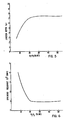
- Figure 2 shows the index of refraction of the coating at the end of this heat treatment as a function of boron concentration in the Ti0 2 based AR precursor solution.
- 8 2 O 3 must be used in the precursor solution.
- a suitable range of dopant concentration is from 1 to 50%.
- a preferred method of adjusting the index of the coating to 2 is to limit the boron addition to less than 30% and to lower the index by the addition of another constituent of low index such as SiO 2 .
- the SiO 2 component may also be added from alkoxides or partially hydrolyzed alkoxides similar to dopant introduction and is described in EP-A-821 5. (The data for Figures 2 to 7 was obtained using procedures described in Example 1. Measurements were done by spreading resistance).
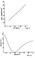
- Figure 7 which illustrates the data of the following table, shows the effect of bake time on the carrier concentration and the junction depth in N-type silicon (10 ohm resistance) for a 10% B 2 O 3 doped AR coating at 900°C in vacuum.
- junction depth can precisely be controlled by heat treatment time.
- a 3.5 weight percent equivalent TiO 2 containing solution was prepared as follows: 1.5 g H Z O, and 130 mg (4 drops) HNO 3 acid were added to 90 g of dry ethyl alcohol, C 2 H 5 OH. Then 10 g of Ti(OC 2 H 5 ) 4 was also added and mixed. A clear solution resulted.
- the indices of refraction of the optical coatings made in Example 1 at various amounts of boron dopings can be reduced to 2 to satisfy the Fresnel condition for antireflectivity on silicon.
- a 10% of silica-containing solution was prepared by hydrolyzing tetraethylsilicate, Si(OC 2 H 5 ) 4 . with 1.8 moles of water in ethanol. Using this solution and the boron and titania solutions described in Example 1 the following AR coating solution was prepared: 21 g, 10 wt. % eq B 2 0 3 containing solution and 10.4 g, 10% eq SiO 2 containing solutions were added to 150 g dry ethanol. 1.5 g H 2 O and 130 mg (4 drops) HN0 3 acid were also introduced. After mixing, 10 g of Ti(OC 2 H 5 ) 4 was added and mixed.
- This solution contained a total of 5 weight percent equivalent oxide which was made up by 70% Tio 2 , 20% B 2 0 3 and 10% SiO z .
- This solution was then spin-coated at 1000 rpm on 1-1/2 inches silicon wafers and heat treated at 900°C in vacuum for 45 minutes.
- Figure 8 shows the spectral reflectivity of the coating which indicates that an ideal single layer antireflective film on silicon has been produced that meets the index of refraction and thickness requirements.
- this sample had a carrier concentration of about 3x10 19 and a junction depth of about 0.5. Junction depth and carrier concentration was extremely uniform on the entire sample.
- Example 2 was repeated with using unhydrolyzed tetraethyl silicon which reacts with the hydroxyl groups of titania. The results were similar except the viscosity of the solution was different, It required an adjustment on the speed of application to obtain quarterwave optical thickness.
- Example 2 was repeated using unhydrolyzed B(OCH 3 ) 3 which again reacts with the hydroxyl groups of titania.
- the results were similar, except that due to the slightly different viscosity of the solution, the coating application rate needed to be different, e.g., 800 rpm.
- Example 2 was repeated using titanium butoxide, Ti(OC 4 H 9 ) 4 and titanium isopropoxide, Ti(OC 3 H 7 ) 4 . Also, various other alcohols were used. The results were similar.
- a 10% e.g. B 2 O 3 doped titania AR coating solution was prepared as described in Example 2. This solution was applied on N-type silicon wafers of .001 ohm per centimeter resistivity at 1000 rpm. The samples were baked at 900°C in vacuum for various lengths of time. The effect of time on carrier concentration, junction depth, and surface resistance for this composition and heat treatment is shown in Table A and Figure 7.
- Example 6 was repeated with 20% boron. The junction depth was found to be 0.50 after baking for 50 minutes and 0.75 after baking for 60 minutes.
- a 3.5 weight percent TiO 2 alkoxide precursor solution was prepared as in Example 1. Phosphoric acid was added to this solution to obtain 15 weight percent equivalent of P 2 0, based on Tio 2 concentration. The solution was applied to boron doped silicon wafers having .001 ohm per centimeter resistivity. The wafers were spun at 1000 rpm then heat treated at 1050°C in nitrogen for one hour. An excellent anti-reflective coating resulted. Tests on the product showed that a suitable phosphorus diffusion took place.
- Example 8 was repeated except 10% phosphorus was introduced from a triethyl phosphate solution. The junction was formed at 1000°C and an excellent antireflective coating with phosphor doping again resulted.
- a solution containing 5% total oxide which was in part made with 70% TiO 2 , 20% B 2 O 3 and 10% Si0 2 as described in Example 2 was prepared and spin coated on an N-type 10-12 ohm resistance silicon wafer 100 cm in diameter at 1000 rpm. The samples were baked at 900°C for 45 minutes and were divided 1 cm 2 photovoltaic cells. The results of these unoptimized cells are shown in the following table.
- sample number 4 was faulty in some respect. It is believed that still higher efficiencies which are listed in the next to the last column will be obtained under optimal conditions.
Description
- In the conventional preparation of a photovoltaic solar cell a PN junction is formed by diffusing either boron or phosphorus into a silicon base material. The silicon base material may be obtained pre-doped so that it is either P type or N type and the opposite type dopant is used in the junction formation process. These diffusions are generally made from a vapor phase in a vacuum or in a non-oxidizing atmosphere such as nitrogen or argon as a carrier gas at temperatures of 850°C to 1100°C.
- In making the solar cells a separate step is needed to apply a quarter-wave optical thickness anti- reflective film to the surface of the cell to make it more efficient. The antireflective coating increases the efficiency of the cell, for example, as much as 50 percent. Such optical coatings are applied by vacuum deposition, sputtering, or other techniques. Recently it was suggested that polymerized titanium dioxide solutions could be made which would deposit optical coatings of the desired thickness and index of refraction by liquid application methods. Examples of the prior art are Patent Abstract of Japan, Vol. 3, No. 106, 7th September 1979, Page 56E135 and JP-A-5 482 992 which describe a method of forming an antireflecting coating of Ti02 (Titania) on a single-crystal silicon wafer, a P-N junction being formed in the wafer by diffusion of dopant impurity from the coating during its formation and US-A-4 101 351 in which a doped 7102 antireflection coating on a silicon substrate is heated to form a diffused P/N junction.
- It is the principal object of the invention to provide an anti-reflective coating to silicon.
- One aspect of the invention resides broadly in a method applying an antireflective coating on silicon comprising the steps of:
- forming a coating of at least 40% titania having dopant properties on said silicon; and
- heating the coated silicon above the diffusion temperature of the dopant, wherein said coating is formed from a clear solution which results from mixing ingredients comprising:
- (A) alkoxide having the general formula M(OR)n where M is selected such that an oxide coating formed from this solution comprises 40 to 100% by weight Tio2, and 0 to 20% by weight Si02, wherein R is alkyl from C1 to C6, and n is the valence of M;
- (B) about 1,7 to about 8 moles of water per mole of alkoxide;
- (C) sufficient alcohol to give a solid content of 0,1 to 15% by weight of the solution;
- (D) a sufficient amount of a suitable acid to prevent cloudiness; and
- (E) 1% to 50% by weight of a P or N dopant, the percentages of the said oxides and the dopant edding up to 100%.
- Another aspect of the invention resides broadly in a silicon chip made according to the above method.
- If an anti-reflective coating is doped with a dopant compound, e.g., boron, the dopant atom will diffuse into the silicon forming a P/N junction during the baking of the antireflective coating. Thus, in a single step, the anti-reflective coating and the P/N junction is simultaneously formed. This eliminates the expensive procedures of diffusing the dopant into the silicon, and numerous other steps related to masking, cleaning, etc. of the substrate, associated with the present methods of diffusion and junction formation. Quite unexpectedly, we have found that the concentration of the dopant in the silicon, which is diffused from titania-based optical coating in our new prcedure, is in the magnitude of 1019 carriers per cm3, which is considered to be the ideal concentration for the optimum results. (Previous techniques had produced concentrations of about 102° or 1022). At these higher concentrations the junction depth had to be limited to only .3 to .4 microns in order to avoid recombination of the charges before they crossed the juncture. Because the technique of this invention results in a lower concentration of dopant in the silicon, control of the junction depth is less critical and juncture depths of one micron or more can be tolerated.
- Another advantage of this process is that extremely uniform dopant diffusion and junction depth can be obtained on large devices, photovoltaic or otherwise. This is due to the fact that the diffusion of dopant occurs from an optical film which is homogeneous in composition at the molecular level and uniform in thickness below the wavelength of light. Still another advantage is that multidopant integration and diffusion on well defined areas of a substrate can be obtained in a single step without the need to mask the substrate; this is done by applying solutions only on those areas.
- An exemplary embodiment of the invention is described infra.
- Figure 1 is a simplified isometric view in section of a certain presently preferred embodiment of a solar cell according to this invention.
- Figures 2 to 8 are graphs which illustrate the results of experiments.
- In Figure 1, a silicon wafer 1 is composed of a
P layer 2, a P/N junction 3, and an N layer 4 from which electricity is drawn bygrids 5 and 6 attached thereto respectively. On the surface of wafer 1 which is exposed to light is the antireflective coating 7 according to this invention, about 1/4 optical wavelength in thickness and having an index of refraction equal to the square-root of the index of refraction of the substrate. The coating reduces the reflection of light back to its source and thereby enhances the efficiency of the solar cell. The captured light causes electrons to move from the P layer to the N layer thereby generating an electric current. - The silicon starting material used in this invention is commercially available in the form of strips, i.e. web silicon, about one-half to one inch in width, and in form of chips about 2 to about 10 centimeters in diameter, though silicon of any dimension can be used. The silicon is commonly about .125 to about .25 mm (5 to 10 mils) in thickness. If undoped silicon is used, it is necessary to diffuse a P layer into the silicon from one surface and an N layer from the opposite surface in order to form a P/N junction. It is preferable to use a silicon material which has been pre-doped with a P or an N dopant throughout because diffusion into this silicon with a dopant of the opposite type forms a P/N junction in one step. Preferably, silicon which has been doped with phosphorus, that is, an N type silicon, is used because it has been found that the method of this invention works best using boron, which is a P type dopant.
- The dopant is diffused into the silicon from a solution derived from metal alkoxides. The precursor solution is a clear titanium oxide based solution, which is derived from partial hydrolysis and polymerization of titanium alkoxides. The preparation of this solution has been presented in detail in European Patent Specification EP-
A-821 5, herein incorporated by reference. Alkoxides useful in preparing the solutions have the general formula iv)(OR)n. In the formula "M" represents a metal ion. This ion is preferably titanium as it is commercially the most important but it can also be tantalum. In this invention at least 40% of the resulting coating should be titania. The remainder can be up to 25% Si02, up to 15% of another metal oxide of a metal which forms an alkoxide, or mixtures thereof. These alkoxides can be included in titania to alter the index of refraction of the coating as will be apparent to those skilled in the art. The small "n" in the formula is the valence of the M ion and can vary from 3 to 5. The R group is alkyl from C1 to Ce. Each R group may be independently selected if desired though they are usually the same. The R group is preferably ethyl, isopropyl, or butyl because these alkoxides are commercially available and inexpensive. Also, the alcohols which are formed from these alkyl groups mix with water in the range of the invention. - The alcohol used in preparing the coating solution can be any liquid solvent or alcohol, so long as it is dry or its water content is low and well defined and it does not react with alkoxides. Higher alcohols produce thicker films. The alcohol need not be the same alcohol that is produced by the hydrolysis of the alkoxide, and in some instances it is desirable that they be different in order to obtain different viscosities. The amount of alcohol used should be sufficient to produce a solution having a solids content of 0.1 to 15% by weight based on equivalent oxide. A greater solids content for the same degree of hydrolysis will cause the solution to gel and a lesser solids content results in undesirably thin coatings. A preferred solids content is about 2 to about 8% by weight based on equivalent oxide. Stated another way, the preferred maximum is about 1 mole alkoxide per liter of final solution.
- Metal alkoxides, in general, hydrolyze quite vigorously when brought into contact with water, forming oxides and hydroxides as represented by the reactions.


- Whether the oxide or the hydroxide forms during the hydrolysis depends on the nature of the alkoxide. In either case, however, the resultant material is particulate, precipitates out, and therefore is not useful for coating. The alkoxides of titanium and tantalum, particularly, form precipitates even under insufficient water hydrolysis, and the formation of precipitates cannot be prevented under normal conditions. However, EP-A-821 5 describes a method of preparing soluble intermediate species from these alkoxides which are capable of polymerizing into an continuous oxide network. Precipitate formation and self-condensation which would normally occur during the hydrolysis of these alkoxides are prevented from occurring by a careful control of molecular interaction during the hydrolysis where certain amounts of OR groups are left in the molecular structure. This is done by controlling, first, the amount of water and dilution of the system, and second, by the presence of a critical amount of certain acids.
- Because the water and/or alkoxide is diluted by the alcohol, the interaction of alkoxide and water molecules are reduced to a critical minimum where the complete hydrolysis of an alkoxide molecule cannot take place, occurrence of which would precipitate Ti02. The first reaction produces a partially hydrolyzed alkoxide which does not precipitate:

- The partially hydrolyzed alkoxide molecules include Ti(OR)2 (OH)2 and Ti(OR)(OH)3 and can then form a polymer with other alkoxide molecules:

- In preparing the solution it is important to avoid contacting alkoxide with water without diluting one or both of them with alcohol first for otherwise a precipitate will form at the point of contact. Although either or both the water and alkoxide can be diluted with alcohol first, it is preferable to dilute the water, then to mix the water-alcohol mixture with the alkoxide. There should be a minimum of 600 cc of alcohol used per mole of alkoxide; the preferable diluting range, however, is 2 to 8 liters of alcohol per mole of alkoxide.
- When water and the alkoxide are brought into contact in an alcohol diluted system, the system turns cloudy. This cloudiness, which indicates the condensation of separate particles, can be avoided by introducing at least 0.014 moles of either HN03 or HCI acids. If the introduction of acid is made into the water-alcohol solution before mixing with the aloxide no cloudiness ever occurs, and this is therefore the preferred method of introducing the acid. Acid can be added anytime after the mixing occurs and it will cause the cloudy slurry to turn into a clear solution. However, if more than 0.1 moles of acid are used per mole of alkoxide, the solubility of the solution is reduced and it will turn cloudy after several days. So far, no organic acids have been found which work, and the only inorganic mineral acids which have been found to work are hydrochloric acid and nitric acid, although not all acids have been tried. It was also found that in some systems, such as in glycol, this acid is not required.
- The dopant compound may be added directly to the alkoxide solution but preferably a separate solution is prepared which contains the dopant compound. The dopant compound is a compound of a P or N type dopant. The commonest N and P dopants are phosphorus and boron and they are preferred as they are the most efficient, but it may be possible to use other dopants such as aluminum or arsenic. Boron is the most preferred dopant because it has been found to work the best. A solution is prepared of a compound of the dopant such as, for example, an alkoxide or an acid. Alkoxides from C, to C4 are preferred. These compounds include boron trimethoxide, boron triethoxide, boron triisopropoxide, phosphorus penta butoxide, phosphorus pentaethoxide, phosphorus pentamethoxide, etc. The three compounds which are particularly preferred are boron trimethoxide, B(OCH3)3, boric acid, and phosphoric acid. Whatever dopant compound is used, it must be compatible with the alkoxide solution. That is, it must go into the precursor solution either by reaction with the metal alkoxide or by dissolution, but it must not form a precipitate. When the alkoxide solution is baked the dopant atoms, boron or phosphorus, migrate into the silicon to form the P/N junction. If the dopant is added from an alkoxide it may be partially hydrolyzed with 1.0 to 1.5 moles of water per mole of alkoxide to prevent its vaporization. However, this may not be necessary if the base solution contains enough hydroxyl groups. The remainder of the solution is made up of alcohol. The alcohol concentration in the total solution controls the thickness of the film but it is not especially critical in the dopant solution and the solution of the dopant compound may contain no alcohol or up to 99% alcohol as is desired. The solution of the dopant compound or the dopant compound itself is then mixed with the alkoxide solution. This final solution should contain about 10% to about 30% by weight of dopant compound based on the total weight of the metal alkoxide and the dopant. More than 30% may be used but there is no additional benefit to using more than 20% because it does not increase the concentration of the dopant in the silicon. However, more may be useful in altering the index of refraction of the coating. Less than 10% reduces the dopant concentration in the silicon but this may be desirable under some circumstances.
- The solution, once prepared, should be aged for a few hours to permit the polymerization to proceed and stabilization of its viscosity. The solution should be clear at this stage. A clear solution indicates that a single continuous phase has been made rather than a particulate suspension or a precipitate. To make a coating from the solution, the solution is applied to a silicon substrate. Application may be by dipping, spraying, printing, painting, spinning, or other suitable liquid application method, but dipping and spinning are the preferred methods as they are most easily adapted to mass production.
- Extremely uniform coatings on large areas, e.g., greater than 100 square centimeters, are readily obtainable, unlike the vapor deposition coating.
- For an anti-reflective coating on a solar cell, the substrate is silicon either in the form of wafers or as a continuous strip. The surface of silicon reflects 35-38% of solar energy; since the reflected portion is not available for the conversion process, the overall efficiency is thereby reduced unless an antireflective coating is applied. Antireflective (AR) coatings must be highly transparent and stable in the outdoor environment. The refractive index and thickness of the AR coating must meet optical conditions described by Fresnel's equation to be antireflective in the desired wavelength range. Minimum reflection from a silicon cell can be achieved by using an AR coating that is of quarter wavelength optical thickness, about 7500 nm (750 A), with an index of refraction of approximately 2.0. Therefore, at the end of the heat treatment, which provides proper boron diffusion and junction depth within the substrate, the coating must meet these optical requirements. Since the coating is affected by this heat-treatment, the initial composition and thickness must be tailored to give the index of
refraction 2 and thickness about (750 A) (7500 nm) after the heat treatment. If a boron or phosphorus dopant is used a preferred temperature range is about 850°C to about 1 100°C because at less than 850°C there is very low diffusion of the boron into the silicon and at more than 1100°C the silicon begins to deteriorate. A temperature of 900°C seems to work the best. The firing should be done in a vacuum or under nitrogen or argon or another inert gas to prevent the silicon from oxidizing. The film resulting after the heat treatment is continuous, has a uniform thickness within several angstroms, and is tenaciously bounded onto the substrate. - For example, a suitable carrier concentration and junction depth is produced for photovottaic sofar application by using N-type silicon (10 to 20 ohms) and diffusing boron from the AR coating at 900°C in vacuum for about 45 minutes. Figure 2 shows the index of refraction of the coating at the end of this heat treatment as a function of boron concentration in the Ti02 based AR precursor solution. As can be seen from Figure 2, for this heat treatment to produce an index close to 2 over 50% 82O3 must be used in the precursor solution. Even though this is acceptable it is noticed that at high B203 concentration, i.e., over 40%, the coating tends to become cloudy, and chemical and environmental resistance may drop. Thus, a suitable range of dopant concentration is from 1 to 50%. A preferred method of adjusting the index of the coating to 2 is to limit the boron addition to less than 30% and to lower the index by the addition of another constituent of low index such as SiO2. The SiO2 component may also be added from alkoxides or partially hydrolyzed alkoxides similar to dopant introduction and is described in EP-
A-821 5. (The data for Figures 2 to 7 was obtained using procedures described in Example 1. Measurements were done by spreading resistance). - The following table, graphically illustrated in Figure 3, shows the amount of equivalent Si02 required to lower the index of refraction to about 2 as a function of amount of B203 dopant present in a titania based AR coating subjected to 900°C vacuum treatment for 45 minutes.

- Additional information on controlling the index of refraction of the metal oxide coating can be found in EP-A-8 215.
- The amount of carrier concentration, spreading resistance, and the junction depth in an N-type silicon substrate (10 ohm resistance) with one hour heat treatment at 900°C in vacuum as a function of B103 concentration in the AR coating are shown in Figures 4, 5, and 6 which illustrate the following table.

- The significance of these figures are, first, that the boron concentration above 20% wt does not affect the carrier concentration nor the junction depth, unlike the boron diffusion done from conventional glass coatings. Secondly and more importantly, the carrier concentration was stabilized at a value in the 1019/cm3 range regardless of the boron present in the AR coating above 20 wt %. This is significant because this value represents the optimized balance between two conflicting factors-the undesirable recombination effect, and the desirable conductivity with increasing carrier concentration. Due to this property of the coatings of this invention, deeper junctions can be obtained with stable carrier concentrations in the method of this invention.
- The effect of time on the carrier concentration appears to be linear at 900°C. Figure 7, which illustrates the data of the following table, shows the effect of bake time on the carrier concentration and the junction depth in N-type silicon (10 ohm resistance) for a 10% B2O3 doped AR coating at 900°C in vacuum.

- This shows that the junction depth can precisely be controlled by heat treatment time.
- A 3.5 weight percent equivalent TiO2 containing solution was prepared as follows: 1.5 g HZO, and 130 mg (4 drops) HNO3 acid were added to 90 g of dry ethyl alcohol, C2H5OH. Then 10 g of Ti(OC2H5)4 was also added and mixed. A clear solution resulted.
- Another clear solution containing trimethyl borate in a partially hydrolyzed form, and containing 10 weight percent equivalent boric oxide, was prepared by adding: 2 g water to 23 g of dry ethyl alcohol. To this 10 g of trimethyl borate, B(OCH3)., was added and mixed. (When more than 1.5 moles of H20 is used per mole boron alkoxide a precipitate results).
- From these two titania and boron solutions, 10, 20, 30, 40, and 50 weight percent equivalent B.2O3 containing solutions were prepared by simply mixing them in proper proportions.
- These solutions were coated on 5 cm silicon wafers by spinning at 2000 rpm. These wafers were then heated at 900°C for 60 minutes in vacuum. The index of refraction of coatings, carrier concentrations, junction depth, and spreading resistance were then measured, which are shown in the following table.

- The indices of refraction of the optical coatings made in Example 1 at various amounts of boron dopings can be reduced to 2 to satisfy the Fresnel condition for antireflectivity on silicon.
- A 10% of silica-containing solution was prepared by hydrolyzing tetraethylsilicate, Si(OC2H5)4. with 1.8 moles of water in ethanol. Using this solution and the boron and titania solutions described in Example 1 the following AR coating solution was prepared: 21 g, 10 wt. % eq B203 containing solution and 10.4 g, 10% eq SiO2 containing solutions were added to 150 g dry ethanol. 1.5 g H2O and 130 mg (4 drops) HN03 acid were also introduced. After mixing, 10 g of Ti(OC2H5)4 was added and mixed.
- This solution contained a total of 5 weight percent equivalent oxide which was made up by 70% Tio2, 20
% B 203 and 10% SiOz. - This solution was then spin-coated at 1000 rpm on 1-1/2 inches silicon wafers and heat treated at 900°C in vacuum for 45 minutes.
- The spectral reflectivity curve measurements were done. Figure 8 shows the spectral reflectivity of the coating which indicates that an ideal single layer antireflective film on silicon has been produced that meets the index of refraction and thickness requirements.
- When the boron diffusion measurements were done, it was found that this sample had a carrier concentration of about 3x10¹⁹ and a junction depth of about 0.5. Junction depth and carrier concentration was extremely uniform on the entire sample.
- Example 2 was repeated with using unhydrolyzed tetraethyl silicon which reacts with the hydroxyl groups of titania. The results were similar except the viscosity of the solution was different, It required an adjustment on the speed of application to obtain quarterwave optical thickness.
- Example 2 was repeated using unhydrolyzed B(OCH3)3 which again reacts with the hydroxyl groups of titania. The results were similar, except that due to the slightly different viscosity of the solution, the coating application rate needed to be different, e.g., 800 rpm.
- Example 2 was repeated using titanium butoxide, Ti(OC4H9)4 and titanium isopropoxide, Ti(OC3H7)4. Also, various other alcohols were used. The results were similar.
- A 10% e.g. B2O3 doped titania AR coating solution was prepared as described in Example 2. This solution was applied on N-type silicon wafers of .001 ohm per centimeter resistivity at 1000 rpm. The samples were baked at 900°C in vacuum for various lengths of time. The effect of time on carrier concentration, junction depth, and surface resistance for this composition and heat treatment is shown in Table A and Figure 7.
- Example 6 was repeated with 20% boron. The junction depth was found to be 0.50 after baking for 50 minutes and 0.75 after baking for 60 minutes.
- A 3.5 weight percent TiO2 alkoxide precursor solution was prepared as in Example 1. Phosphoric acid was added to this solution to obtain 15 weight percent equivalent of P20, based on Tio2 concentration. The solution was applied to boron doped silicon wafers having .001 ohm per centimeter resistivity. The wafers were spun at 1000 rpm then heat treated at 1050°C in nitrogen for one hour. An excellent anti-reflective coating resulted. Tests on the product showed that a suitable phosphorus diffusion took place.
- Example 8 was repeated except 10% phosphorus was introduced from a triethyl phosphate solution. The junction was formed at 1000°C and an excellent antireflective coating with phosphor doping again resulted.
- A solution containing 5% total oxide which was in part made with 70% TiO2, 20% B2O3 and 10% Si02 as described in Example 2 was prepared and spin coated on an N-type 10-12 ohm resistance silicon wafer 100 cm in diameter at 1000 rpm. The samples were baked at 900°C for 45 minutes and were divided 1 cm2 photovoltaic cells. The results of these unoptimized cells are shown in the following table.
- In the following table, sample number 4 was faulty in some respect. It is believed that still higher efficiencies which are listed in the next to the last column will be obtained under optimal conditions.

Claims (12)
Applications Claiming Priority (2)
| Application Number | Priority Date | Filing Date | Title |
|---|---|---|---|
| US06/066,368 US4251285A (en) | 1979-08-14 | 1979-08-14 | Diffusion of dopant from optical coating and single step formation of PN junction in silicon solar cell and coating thereon |
| US66368 | 1987-06-25 |
Publications (2)
| Publication Number | Publication Date |
|---|---|
| EP0024057A1 EP0024057A1 (en) | 1981-02-18 |
| EP0024057B1 true EP0024057B1 (en) | 1984-03-21 |
Family
ID=22069056
Family Applications (1)
| Application Number | Title | Priority Date | Filing Date |
|---|---|---|---|
| EP80104848A Expired EP0024057B1 (en) | 1979-08-14 | 1980-08-14 | Single step formation of pn junction in silicon cell and coating thereon |
Country Status (14)
| Country | Link |
|---|---|
| US (1) | US4251285A (en) |
| EP (1) | EP0024057B1 (en) |
| JP (1) | JPS5660075A (en) |
| KR (1) | KR830002294B1 (en) |
| AU (1) | AU537352B2 (en) |
| BR (1) | BR8005034A (en) |
| DE (1) | DE3067142D1 (en) |
| ES (1) | ES8106817A1 (en) |
| HK (1) | HK29385A (en) |
| IL (1) | IL60807A (en) |
| IN (1) | IN152740B (en) |
| MX (1) | MX155893A (en) |
| MY (1) | MY8500900A (en) |
| ZA (1) | ZA804634B (en) |
Cited By (2)
| Publication number | Priority date | Publication date | Assignee | Title |
|---|---|---|---|---|
| US8507837B2 (en) | 2008-10-24 | 2013-08-13 | Suncore Photovoltaics, Inc. | Techniques for monitoring solar array performance and applications thereof |
| US8513514B2 (en) | 2008-10-24 | 2013-08-20 | Suncore Photovoltaics, Inc. | Solar tracking for terrestrial solar arrays with variable start and stop positions |
Families Citing this family (48)
| Publication number | Priority date | Publication date | Assignee | Title |
|---|---|---|---|---|
| US4619719A (en) * | 1982-01-28 | 1986-10-28 | Owens-Illinois, Inc. | Process for forming a doped oxide film and composite article |
| US4571366A (en) * | 1982-02-11 | 1986-02-18 | Owens-Illinois, Inc. | Process for forming a doped oxide film and doped semiconductor |
| US4605450A (en) * | 1982-02-11 | 1986-08-12 | Owens-Illinois, Inc. | Process for forming a doped oxide film and doped semiconductor |
| DE3340874A1 (en) * | 1983-11-11 | 1985-05-23 | Telefunken electronic GmbH, 7100 Heilbronn | METHOD FOR PRODUCING A SOLAR CELL |
| JPS60140880A (en) * | 1983-12-28 | 1985-07-25 | Hitachi Ltd | Manufacture of solar cell |
| US4744973A (en) * | 1985-11-29 | 1988-05-17 | Westinghouse Electric Corp. | Inorganic polymeric cationic ion exchange matrix |
| US4808464A (en) * | 1987-07-23 | 1989-02-28 | Westinghouse Electric Corp. | Insulating ferromagnetic amorphous metal strips |
| US4759949A (en) * | 1987-07-23 | 1988-07-26 | Westinghouse Electric Corp. | Method of insulating ferromagnetic amorphous metal continuous strip |
| JPH0690014A (en) * | 1992-07-22 | 1994-03-29 | Mitsubishi Electric Corp | Thin solar cell and its production, etching method and automatic etching device, and production of semiconductor device |
| US5270248A (en) * | 1992-08-07 | 1993-12-14 | Mobil Solar Energy Corporation | Method for forming diffusion junctions in solar cell substrates |
| US5478776A (en) * | 1993-12-27 | 1995-12-26 | At&T Corp. | Process for fabricating integrated circuit containing shallow junction using dopant source containing organic polymer or ammonium silicate |
| JP3032422B2 (en) * | 1994-04-28 | 2000-04-17 | シャープ株式会社 | Solar cell and method of manufacturing the same |
| US5792280A (en) * | 1994-05-09 | 1998-08-11 | Sandia Corporation | Method for fabricating silicon cells |
| AUPM996094A0 (en) * | 1994-12-08 | 1995-01-05 | Pacific Solar Pty Limited | Multilayer solar cells with bypass diode protection |
| US6278053B1 (en) * | 1997-03-25 | 2001-08-21 | Evergreen Solar, Inc. | Decals and methods for providing an antireflective coating and metallization on a solar cell |
| US7090890B1 (en) | 1998-04-13 | 2006-08-15 | The Trustees Of Princeton University | Modification of polymer optoelectronic properties after film formation by impurity addition or removal |
| KR20010042689A (en) * | 1998-04-13 | 2001-05-25 | 트러스티스 오브 프린스턴 유니버시티 | Modification of polymer optoelectronic properties after film formation impurity addition or removal |
| AUPP437598A0 (en) * | 1998-06-29 | 1998-07-23 | Unisearch Limited | A self aligning method for forming a selective emitter and metallization in a solar cell |
| JP4812147B2 (en) * | 1999-09-07 | 2011-11-09 | 株式会社日立製作所 | Manufacturing method of solar cell |
| US7402448B2 (en) * | 2003-01-31 | 2008-07-22 | Bp Corporation North America Inc. | Photovoltaic cell and production thereof |
| US20080057686A1 (en) * | 2006-08-31 | 2008-03-06 | Melgaard Hans L | Continuous dopant addition |
| US9012766B2 (en) | 2009-11-12 | 2015-04-21 | Silevo, Inc. | Aluminum grid as backside conductor on epitaxial silicon thin film solar cells |
| KR20120085333A (en) * | 2009-12-28 | 2012-07-31 | 샤프 가부시키가이샤 | Method for manufacturing a solar cell |
| US20120318340A1 (en) * | 2010-05-04 | 2012-12-20 | Silevo, Inc. | Back junction solar cell with tunnel oxide |
| US9214576B2 (en) | 2010-06-09 | 2015-12-15 | Solarcity Corporation | Transparent conducting oxide for photovoltaic devices |
| US9773928B2 (en) | 2010-09-10 | 2017-09-26 | Tesla, Inc. | Solar cell with electroplated metal grid |
| US9800053B2 (en) | 2010-10-08 | 2017-10-24 | Tesla, Inc. | Solar panels with integrated cell-level MPPT devices |
| JP5723143B2 (en) * | 2010-12-06 | 2015-05-27 | シャープ株式会社 | Manufacturing method of back electrode type solar cell and back electrode type solar cell |
| US9054256B2 (en) | 2011-06-02 | 2015-06-09 | Solarcity Corporation | Tunneling-junction solar cell with copper grid for concentrated photovoltaic application |
| JP2013026524A (en) * | 2011-07-22 | 2013-02-04 | Hitachi Chem Co Ltd | N-type diffusion layer forming composition, manufacturing method of n-type diffusion layer, manufacturing method of solar cell element, and solar cell |
| WO2013043809A2 (en) * | 2011-09-21 | 2013-03-28 | Arizona Board Of Regents, A Body Corporate Of The State Of Arizona | Heterostructure si solar cells using wide-bandgap semiconductors |
| KR101381844B1 (en) * | 2012-04-24 | 2014-04-24 | 에스티엑스 솔라주식회사 | Method for menufacture the bifacial solar cell |
| EP2904643B1 (en) | 2012-10-04 | 2018-12-05 | SolarCity Corporation | Solar cell with electroplated metal grid |
| US9865754B2 (en) | 2012-10-10 | 2018-01-09 | Tesla, Inc. | Hole collectors for silicon photovoltaic cells |
| US9281436B2 (en) | 2012-12-28 | 2016-03-08 | Solarcity Corporation | Radio-frequency sputtering system with rotary target for fabricating solar cells |
| US9219174B2 (en) | 2013-01-11 | 2015-12-22 | Solarcity Corporation | Module fabrication of solar cells with low resistivity electrodes |
| US10074755B2 (en) | 2013-01-11 | 2018-09-11 | Tesla, Inc. | High efficiency solar panel |
| US9412884B2 (en) | 2013-01-11 | 2016-08-09 | Solarcity Corporation | Module fabrication of solar cells with low resistivity electrodes |
| US9624595B2 (en) | 2013-05-24 | 2017-04-18 | Solarcity Corporation | Electroplating apparatus with improved throughput |
| US10309012B2 (en) | 2014-07-03 | 2019-06-04 | Tesla, Inc. | Wafer carrier for reducing contamination from carbon particles and outgassing |
| US9899546B2 (en) | 2014-12-05 | 2018-02-20 | Tesla, Inc. | Photovoltaic cells with electrodes adapted to house conductive paste |
| US9947822B2 (en) | 2015-02-02 | 2018-04-17 | Tesla, Inc. | Bifacial photovoltaic module using heterojunction solar cells |
| US9761744B2 (en) | 2015-10-22 | 2017-09-12 | Tesla, Inc. | System and method for manufacturing photovoltaic structures with a metal seed layer |
| US9842956B2 (en) | 2015-12-21 | 2017-12-12 | Tesla, Inc. | System and method for mass-production of high-efficiency photovoltaic structures |
| US9496429B1 (en) | 2015-12-30 | 2016-11-15 | Solarcity Corporation | System and method for tin plating metal electrodes |
| US10115838B2 (en) | 2016-04-19 | 2018-10-30 | Tesla, Inc. | Photovoltaic structures with interlocking busbars |
| US10672919B2 (en) | 2017-09-19 | 2020-06-02 | Tesla, Inc. | Moisture-resistant solar cells for solar roof tiles |
| US11190128B2 (en) | 2018-02-27 | 2021-11-30 | Tesla, Inc. | Parallel-connected solar roof tile modules |
Family Cites Families (6)
| Publication number | Priority date | Publication date | Assignee | Title |
|---|---|---|---|---|
| US3437527A (en) * | 1966-10-26 | 1969-04-08 | Webb James E | Method for producing a solar cell having an integral protective covering |
| US3460956A (en) * | 1968-07-19 | 1969-08-12 | Joseph Dahle | Titanate product and method of making the same |
| US3993506A (en) * | 1975-09-25 | 1976-11-23 | Varian Associates | Photovoltaic cell employing lattice matched quaternary passivating layer |
| US4101351A (en) * | 1976-11-15 | 1978-07-18 | Texas Instruments Incorporated | Process for fabricating inexpensive high performance solar cells using doped oxide junction and insitu anti-reflection coatings |
| JPS5482992A (en) * | 1977-12-14 | 1979-07-02 | Sharp Corp | Solar battery and its manufacture |
| IN152814B (en) * | 1978-08-08 | 1984-04-14 | Westinghouse Electric Corp |
-
1979
- 1979-08-14 US US06/066,368 patent/US4251285A/en not_active Expired - Lifetime
-
1980
- 1980-07-30 ZA ZA00804634A patent/ZA804634B/en unknown
- 1980-08-01 AU AU61001/80A patent/AU537352B2/en not_active Ceased
- 1980-08-02 IN IN882/CAL/80A patent/IN152740B/en unknown
- 1980-08-04 MX MX183426A patent/MX155893A/en unknown
- 1980-08-08 IL IL60807A patent/IL60807A/en not_active IP Right Cessation
- 1980-08-11 BR BR8005034A patent/BR8005034A/en not_active IP Right Cessation
- 1980-08-13 ES ES494214A patent/ES8106817A1/en not_active Expired
- 1980-08-14 KR KR1019800003221A patent/KR830002294B1/en active
- 1980-08-14 EP EP80104848A patent/EP0024057B1/en not_active Expired
- 1980-08-14 JP JP11117080A patent/JPS5660075A/en active Pending
- 1980-08-14 DE DE8080104848T patent/DE3067142D1/en not_active Expired
-
1985
- 1985-04-11 HK HK293/85A patent/HK29385A/en unknown
- 1985-12-30 MY MY900/85A patent/MY8500900A/en unknown
Non-Patent Citations (1)
| Title |
|---|
| JOURNAL OF THE ELECTROCHEMICAL SOCIETY, vol. 125, no. 6, June 1978, pages 983-985, New York, U.S.A. H.J. HOVEL: "TiO2 Antireflection Coatings by a Low Temperature Spray Process" * |
Cited By (4)
| Publication number | Priority date | Publication date | Assignee | Title |
|---|---|---|---|---|
| US8946608B2 (en) | 2008-02-01 | 2015-02-03 | Suncore Photovoltaics, Inc. | Solar tracking system |
| US8507837B2 (en) | 2008-10-24 | 2013-08-13 | Suncore Photovoltaics, Inc. | Techniques for monitoring solar array performance and applications thereof |
| US8513514B2 (en) | 2008-10-24 | 2013-08-20 | Suncore Photovoltaics, Inc. | Solar tracking for terrestrial solar arrays with variable start and stop positions |
| US8890044B2 (en) | 2008-10-24 | 2014-11-18 | Suncore Photovoltaics, Incorporated | Solar cell system |
Also Published As
| Publication number | Publication date |
|---|---|
| HK29385A (en) | 1985-04-19 |
| AU537352B2 (en) | 1984-06-21 |
| DE3067142D1 (en) | 1984-04-26 |
| KR830003804A (en) | 1983-06-22 |
| EP0024057A1 (en) | 1981-02-18 |
| JPS5660075A (en) | 1981-05-23 |
| IL60807A0 (en) | 1980-10-26 |
| ES494214A0 (en) | 1981-08-01 |
| MY8500900A (en) | 1985-12-31 |
| US4251285A (en) | 1981-02-17 |
| KR830002294B1 (en) | 1983-10-21 |
| IN152740B (en) | 1984-03-24 |
| ZA804634B (en) | 1981-07-29 |
| BR8005034A (en) | 1981-02-24 |
| AU6100180A (en) | 1981-02-19 |
| MX155893A (en) | 1988-05-18 |
| ES8106817A1 (en) | 1981-08-01 |
| IL60807A (en) | 1983-10-31 |
Similar Documents
| Publication | Publication Date | Title |
|---|---|---|
| EP0024057B1 (en) | Single step formation of pn junction in silicon cell and coating thereon | |
| US4346131A (en) | Polymerized solutions for depositing optical oxide coatings | |
| US4361598A (en) | Polymerized solutions for depositing optical oxide coatings | |
| Brinker et al. | Sol-gel derived antireflective coatings for silicon | |
| US7659475B2 (en) | Method for backside surface passivation of solar cells and solar cells with such passivation | |
| JP2017120873A (en) | Insulating paste, method for producing the same, and method for manufacturing solar cell element | |
| EP0008215B1 (en) | Polymerized solutions of an oxide; method of preparation thereof; method of preparing alkoxyde coatings on substrates, such as solar cells, and product so obtained | |
| US4571366A (en) | Process for forming a doped oxide film and doped semiconductor | |
| US10693021B2 (en) | Method of passivating a silicon substrate for use in a photovoltaic device | |
| US8864898B2 (en) | Coating formulations for optical elements | |
| US10749047B2 (en) | Solar cell element and method for manufacturing solar cell element | |
| CN109153787B (en) | Polysiloxane, material for semiconductor, semiconductor and solar cell preparation method | |
| Szlufcik et al. | Screen-printed titanium dioxide anti-reflection coating for silicon solar cells | |
| KR101198930B1 (en) | Method for preparing silicon nitride anti-reflection coating and silicon solar cell using the same | |
| JP2017069247A (en) | Insulating paste, manufacturing method of the same, and manufacturing method of solar cell element | |
| US20150083209A1 (en) | Coatable diffusing agent composition, method for producing coatable diffusing agent composition, solar cell, and method for manufacturing solar cell | |
| Yoldas | Diffusion of Dopants from Optical Coatings and Single Step Formation of Antireflective Coating and P‐N Junction in Photovoltaic Cells | |
| JP6971769B2 (en) | Solar cell element | |
| KR101133953B1 (en) | Method for preparing silica anti-reflection coating and silicon solar cell using the same | |
| JPS623597B2 (en) | ||
| TWI630725B (en) | Method for forming surface film and solar cell with surface film | |
| EP0291009A2 (en) | Formation of superconductive ceramic oxides by chemical polymerization | |
| JP6893438B2 (en) | Insulating paste used to form a protective layer in the manufacture of solar cell elements | |
| TW201703855A (en) | Printable pasty diffusion and alloying barrier for the production of highly efficient crystalline silicon solar cells |
Legal Events
| Date | Code | Title | Description |
|---|---|---|---|
| PUAI | Public reference made under article 153(3) epc to a published international application that has entered the european phase |
Free format text: ORIGINAL CODE: 0009012 |
|
| AK | Designated contracting states |
Designated state(s): BE CH DE FR GB IT NL SE |
|
| 17P | Request for examination filed |
Effective date: 19810806 |
|
| ITF | It: translation for a ep patent filed |
Owner name: ING. ZINI MARANESI & C. S.R.L. |
|
| GRAA | (expected) grant |
Free format text: ORIGINAL CODE: 0009210 |
|
| AK | Designated contracting states |
Designated state(s): BE CH DE FR GB IT LI NL SE |
|
| REF | Corresponds to: |
Ref document number: 3067142 Country of ref document: DE Date of ref document: 19840426 |
|
| ET | Fr: translation filed | ||
| PLBE | No opposition filed within time limit |
Free format text: ORIGINAL CODE: 0009261 |
|
| STAA | Information on the status of an ep patent application or granted ep patent |
Free format text: STATUS: NO OPPOSITION FILED WITHIN TIME LIMIT |
|
| 26N | No opposition filed | ||
| ITTA | It: last paid annual fee | ||
| PG25 | Lapsed in a contracting state [announced via postgrant information from national office to epo] |
Ref country code: FR Effective date: 19930430 |
|
| PGFP | Annual fee paid to national office [announced via postgrant information from national office to epo] |
Ref country code: FR Payment date: 19930608 Year of fee payment: 14 |
|
| REG | Reference to a national code |
Ref country code: FR Ref legal event code: ST |
|
| PGFP | Annual fee paid to national office [announced via postgrant information from national office to epo] |
Ref country code: CH Payment date: 19940620 Year of fee payment: 15 |
|
| PGFP | Annual fee paid to national office [announced via postgrant information from national office to epo] |
Ref country code: SE Payment date: 19940627 Year of fee payment: 15 Ref country code: GB Payment date: 19940627 Year of fee payment: 15 |
|
| PGFP | Annual fee paid to national office [announced via postgrant information from national office to epo] |
Ref country code: BE Payment date: 19940714 Year of fee payment: 15 |
|
| PGFP | Annual fee paid to national office [announced via postgrant information from national office to epo] |
Ref country code: NL Payment date: 19940831 Year of fee payment: 15 |
|
| PGFP | Annual fee paid to national office [announced via postgrant information from national office to epo] |
Ref country code: DE Payment date: 19940930 Year of fee payment: 15 |
|
| EAL | Se: european patent in force in sweden |
Ref document number: 80104848.9 |
|
| PG25 | Lapsed in a contracting state [announced via postgrant information from national office to epo] |
Ref country code: GB Effective date: 19950814 |
|
| PG25 | Lapsed in a contracting state [announced via postgrant information from national office to epo] |
Ref country code: SE Effective date: 19950815 |
|
| PG25 | Lapsed in a contracting state [announced via postgrant information from national office to epo] |
Ref country code: LI Effective date: 19950831 Ref country code: CH Effective date: 19950831 Ref country code: BE Effective date: 19950831 |
|
| BERE | Be: lapsed |
Owner name: WESTINGHOUSE ELECTRIC CORP. Effective date: 19950831 |
|
| PG25 | Lapsed in a contracting state [announced via postgrant information from national office to epo] |
Ref country code: NL Effective date: 19960301 |
|
| GBPC | Gb: european patent ceased through non-payment of renewal fee |
Effective date: 19950814 |
|
| REG | Reference to a national code |
Ref country code: CH Ref legal event code: PL |
|
| NLV4 | Nl: lapsed or anulled due to non-payment of the annual fee |
Effective date: 19960301 |
|
| PG25 | Lapsed in a contracting state [announced via postgrant information from national office to epo] |
Ref country code: DE Effective date: 19960501 |
|
| EUG | Se: european patent has lapsed |
Ref document number: 80104848.9 |