EP0021894B1 - Procédé et dispositif d'interconnexions de composants électroniques - Google Patents
Procédé et dispositif d'interconnexions de composants électroniques Download PDFInfo
- Publication number
- EP0021894B1 EP0021894B1 EP80400764A EP80400764A EP0021894B1 EP 0021894 B1 EP0021894 B1 EP 0021894B1 EP 80400764 A EP80400764 A EP 80400764A EP 80400764 A EP80400764 A EP 80400764A EP 0021894 B1 EP0021894 B1 EP 0021894B1
- Authority
- EP
- European Patent Office
- Prior art keywords
- wire
- clip
- soldering
- blade
- support
- Prior art date
- Legal status (The legal status is an assumption and is not a legal conclusion. Google has not performed a legal analysis and makes no representation as to the accuracy of the status listed.)
- Expired
Links
Images

Classifications
-
- H—ELECTRICITY
- H05—ELECTRIC TECHNIQUES NOT OTHERWISE PROVIDED FOR
- H05K—PRINTED CIRCUITS; CASINGS OR CONSTRUCTIONAL DETAILS OF ELECTRIC APPARATUS; MANUFACTURE OF ASSEMBLAGES OF ELECTRICAL COMPONENTS
- H05K13/00—Apparatus or processes specially adapted for manufacturing or adjusting assemblages of electric components
- H05K13/06—Wiring by machine
-
- H—ELECTRICITY
- H05—ELECTRIC TECHNIQUES NOT OTHERWISE PROVIDED FOR
- H05K—PRINTED CIRCUITS; CASINGS OR CONSTRUCTIONAL DETAILS OF ELECTRIC APPARATUS; MANUFACTURE OF ASSEMBLAGES OF ELECTRICAL COMPONENTS
- H05K3/00—Apparatus or processes for manufacturing printed circuits
- H05K3/22—Secondary treatment of printed circuits
- H05K3/222—Completing of printed circuits by adding non-printed jumper connections
-
- Y—GENERAL TAGGING OF NEW TECHNOLOGICAL DEVELOPMENTS; GENERAL TAGGING OF CROSS-SECTIONAL TECHNOLOGIES SPANNING OVER SEVERAL SECTIONS OF THE IPC; TECHNICAL SUBJECTS COVERED BY FORMER USPC CROSS-REFERENCE ART COLLECTIONS [XRACs] AND DIGESTS
- Y10—TECHNICAL SUBJECTS COVERED BY FORMER USPC
- Y10T—TECHNICAL SUBJECTS COVERED BY FORMER US CLASSIFICATION
- Y10T29/00—Metal working
- Y10T29/49—Method of mechanical manufacture
- Y10T29/49002—Electrical device making
- Y10T29/49117—Conductor or circuit manufacturing
- Y10T29/49124—On flat or curved insulated base, e.g., printed circuit, etc.
- Y10T29/49128—Assembling formed circuit to base
-
- Y—GENERAL TAGGING OF NEW TECHNOLOGICAL DEVELOPMENTS; GENERAL TAGGING OF CROSS-SECTIONAL TECHNOLOGIES SPANNING OVER SEVERAL SECTIONS OF THE IPC; TECHNICAL SUBJECTS COVERED BY FORMER USPC CROSS-REFERENCE ART COLLECTIONS [XRACs] AND DIGESTS
- Y10—TECHNICAL SUBJECTS COVERED BY FORMER USPC
- Y10T—TECHNICAL SUBJECTS COVERED BY FORMER US CLASSIFICATION
- Y10T29/00—Metal working
- Y10T29/53—Means to assemble or disassemble
- Y10T29/5313—Means to assemble electrical device
- Y10T29/532—Conductor
- Y10T29/53209—Terminal or connector
- Y10T29/53213—Assembled to wire-type conductor
Definitions
- the present invention relates to a method for producing an electrical interconnection circuit for electronic components, as well as a device for implementing this method.
- the miniaturized electronic components are generally fixed on an insulating base support on which the various electrical interconnections between these components are made.
- it is necessary to have a maximum number of components on a surface of the base support as small as possible. This result can only be obtained by miniaturizing the electrical connections and using insulated wires, the installation of which can be carried out automatically and the layout of which can be modified on demand.
- a number of methods and devices are known for making electrical interconnection circuits between different electronic components automatically and according to programmable paths.
- these known devices are generally complex when they make it possible to obtain a suitable miniaturization of the interconnection circuits, while the simpler devices do not make it possible to obtain a satisfactory density of components taking into account the miniaturization of these. this.
- Document FR-A-2 191 399 already discloses such a method according to which an insulating base support is used comprising conductive zones, the zones to be interconnected are joined together by an insulated heat-sealable wire by bonding it to the base support, solder the bare wire to the conductive areas, and cut it after welding.
- This method has the advantage of late filing of the interconnection wires, which makes it possible to modify the interconnection circuit on demand from standardized cards prepared in advance.
- Document US-A-3 842 190 also discloses a method for making interconnections by means of an insulated wire, the ends of which are welded to conductive zones each having a part intended to receive the welded wire and a part capable of contacting a tab of an electronic component.
- the soldering must be carried out on a conductive pad of relatively large dimensions (of the order of 2 mm in diameter), so that this heating time does not have damaging consequences such as detachment and degradation of the tablet.
- the size of the interconnection circuit obtained with such a device is therefore not sufficiently reduced to allow optimum use of the miniaturized electronic components currently available, and this device is therefore not suitable for a process for automatic production of the interconnection circuit. between these components.
- a method for producing an electrical interconnection circuit on an insulating base support comprising conductive zones capable of receiving electronic components, in which the areas to be interconnected are joined by an insulated heat-sealable wire which is cut after soldering, this process being characterized in that liquid flux is deposited on the parts of the soldering wire resting on the conductive areas before to carry out the welding, in order to reduce the heating time.
- the invention makes it possible to dispense with a separate tinning operation of the insulated wire.
- the invention makes it possible to significantly reduce the heating time, the heat induced by the iron being communicated very quickly to the entire external surface of the wire and to the adjacent surface.
- the conductive pad which allows the stripping of the wire in the same operation as well as accelerating the melting of the layer of lead tin deposited on the conductive pad in order to perform the soldering, while limiting oxidation bare wire and tin.
- the dimensions of the conductive pad can therefore be significantly reduced compared to the dimensions of the pads used in the known prior device using a heat-sealable insulating wire.
- the non-welded end of the cut wire is gripped and brought to a conductive area in order to start another interconnection.
- This characteristic makes it possible to achieve precise positioning and retention of the wire with respect to the conductive patch on which it is to be welded.
- the insulating base support comprising groups of aligned conductive zones capable of receiving electronic boxes provided with two series of aligned tabs and the conductive areas comprising pads each defining a connection pad capable of receiving a tab of one.
- housing, and a wire welding zone juxtaposed with the connection pad, the connection pad and the wire welding zone are arranged in the direction defined by the group of corresponding conductive zones, each pad being cut so as to present a zone of reduced width playing the role of a thermal resistance between the connection pad and the welding zone. This avoids the flow of lead tin into the hole intended to receive the tab of the housing, the latter not yet being mounted during welding.
- each patch can also be contained in a square whose side is substantially equal to 3/5 ° of the distance separating the center of two successive conducting zones of the same group, the connection pad and the welding zone occupying in this square two juxtaposed rectangles whose respective surfaces are substantially equal to 2/3 and 1/3 of the total area of the square.
- the invention also relates to an improvement to a device for producing an electrical interconnection circuit for electronic components, having the function of connecting by conductive wires isolated from the conductive areas situated on a base support possibly covered with adhesive resin outside.
- said conductive zones this device comprising an XY table, the insulating base support being integral with said table, means for controlling the translations of said XY table in two perpendicular directions, a head consisting of a fixed barrel and a rotary frame linked to the barrel, means for controlling the rotation of the frame around an axis perpendicular to the support, means integral with the fixed barrel for unwinding a heat-sealable wire, and means integral with the rotary frame for applying the wire to the support, strip and solder the wire on the conductive areas and cut the wire after welding, this improvement being characterized in that the head The tool holder also carries means for depositing on the welding wire resting on a conductive area a determined quantity of flux to be welded.
- the means for depositing a determined quantity of flux to be welded comprise a movable arm provided with a curved end and a constant level flux reservoir in which the curved end of the arm is at rest in permanent contact with the flow.
- the device defined above further comprises means for gripping the non-welded end of the cut wire.
- these means comprise a clamp and the means for cutting the wire comprise a knife, the clamp being carried by the knife and provided with a curved end movable in a direction normal to the base support relative to the knife, the movement of the curved end of the forceps relative to the knife controlling the opening and closing of the forceps.
- the curved end of the forceps protrudes beyond the edge of the knife when the forceps are open, so that the implementation of the knife causes the abutment of the 'curved end of the clamp against the base support, then the movement of the knife relative to the end of the clamp in the direction corresponding to the closing thereof.
- the means for stripping and soldering the wire comprise a stop capable of coming to come flush with a stop opposite, formed on the clamp during their implementation, so that the displacement of the knife away from the base support causes the clamp to come into abutment against the stop formed on the means for stripping and welding the wire, then the displacement of the knife relative to the end of the clamp in the direction corresponding to the opening of it.
- the end of the forceps may comprise two jaws facing each other elastically urged away from one another and defining on their opposite edges cam surfaces with which cooperate fingers rigidly fixed to the knife, the shape of the cam surfaces being such that the clamp is open when its end projects beyond the edge of the knife and closed when its end is substantially aligned with the edge of the knife.
- the clamp is then made of a preformed elastic wire, such as a piano cord, folded in a U shape to define the jaws of the clamp by its two diamond-shaped ends, the elastic wire being fixed to the knife.
- the fingers attached to the knife cooperating with the jaws in the vicinity of the acute angle of the rhombus opposite the end of the forceps, when the latter projects beyond the edge of the knife, and cooperating with the jaw in the vicinity of the obtuse angles of the rhombus, and on the side of the end of the forceps when the latter is substantially aligned with the edge of the knife.
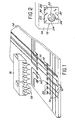
- the invention aims to allow the realization of a circuit comprising a number of electrical interconnections, by means of connecting wires 10 electrically connecting conductive areas 12 fixed on one of the faces of an insulating base support 14, this circuit being capable of receiving a certain number of miniaturized electronic components such as the housing 16.
- the electronic components 16 which are designed to be mounted on the support 14 include lugs 18 received in holes 20 passing through the support 14 and the conductive areas 12, so as to allow the fixing of these components, for example by welding, and their interconnection according to an electrical circuit defined in advance, via the conductive areas 12 and connecting wires 10, the latter being glued to the support 14 and welded to the zones 12 before the components are assembled, according to a process which will be described later.
- the connecting wires 10 are conductive wires such as insulated and heat-welded copper wires.
- the insulator consists, for example, of a layer of polyurethane varnish having the property of volatilizing very quickly, that is to say in one second at 400 ° C. and in three seconds at 380 ° C.
- thermosetting adhesive is deposited on the face of the support 14 intended to receive the wires and the components.
- This adhesive can be deposited on all the non-conducting parts of this face by any known means.
- it can be a dry film which adheres to the support by heating, the holes corresponding to the conducting zones being made before or after depositing the film on the support, free by screen printing.
- the resin can also be deposited in solution, by screen printing, or else in the form of a continuous photosensitive film etched by chemical means, for example after exposure of the areas to be preserved through a photographic mask.
- the adhesive can also be hardenable. It can thus be deposited locally by the machine or preexist on the wire.
- the connecting wires 10 must in no case be placed on the conductive zones 12 corresponding to unconnected electronic components.
- these wires must be arranged either horizontally, vertically, or at 45 °, between the rows formed by the conductive zones 12, as shown in FIG. 1.
- the conductive zones 12 each include a patch 22 defining a connection pad 24, and a welding zone 28.
- the walls of the hole 20 intended to receive one of the legs 18 of component 16 are metallized as shown in 26.
- the welding zone 28 is juxtaposed with the connection pad 24 and separated from the latter by opposite triangular notches 30 defining between them a thermal resistance whose function will appear in the following description.
- the wafer 22 is constituted by a copper layer of about 35 .... thick covered with a layer of tin-lead at least 25 (i thick which allows the welding of the wires 10 without the addition of tin.
- each of the pads 22 is juxtaposed with the connection pad 24 in the direction defined by the corresponding group of conductive zones 12, as illustrated in FIG. 1.
- each of the pads 22 is contained in a square whose side is substantially equal to 3/5 of the distance separating the center of two successive conducting zones 12 of the same group, the connection pad 24 and the welding zone 28 occupying in this square two juxtaposed rectangles whose respective surfaces are substantially equal to 2/3 and to 1 / 3 of the total area of the square as shown in particular in FIG. 2.
- the distance separating the center of two successive conducting zones 12 of the same group is normalized and equal to 2 , 54 mm, so that the patch 22 is then inscribed in a square whose side is equal to 1.524 mm, which then makes it possible to pass up to two connecting wires 10 between two successive conducting zones 12 of the same group, as shown in Figure 1, for a spacing between wires of 0.508 mm.
- 0.254 mm for example, we could pass three and even four sons.
- the structure, the arrangement and the dimensioning of the pellets 22 which have just been described make it possible to substantially improve the density of components on the support 14, thirty boxes of the type of the box 16 can be placed on 1 dm 2 of support.
- pads 22 of reduced surface area is made possible by the method of producing the interconnection circuit 10 according to the invention.
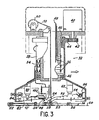
- FIG. 3 This method implements a device shown diagrammatically in FIG. 3, which comprises a tool-carrying head, generally designated by the reference 32.
- the tool-carrying head 32 is composed pr: ncipaiement of a fixed central barrel 34 connected electrically by rotary contacts 36 to a rotating frame 38, the latter being driven by an electric motor 40 via a pinion 42 acting on a toothed wheel 44 secured to the frame 38.
- the rotating frame 38 is supported by the barrel central 34 by means of two bearings 46.
- the central barrel 34 carries the electrical supply (not shown) of the various tools, the delivered voltage arriving by the wires 48.
- the barrel 34 also carries a supply system 50 of wires insulators 10.
- the rotating frame 38 carries an arm 52, by means of a pivot 54 on which is mounted a torsion spring 56 urging by a roller 58 mounted at the free end of the arm 52 the wire 10 against the support 14, this the latter being mounted on a table 60.
- An electromagnet 62 is capable of urging the arm 52 upwards when considering FIG. 3, so as to move the caster 58 away from the support 14 against the force exerted by the spring 56.
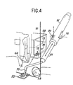
- the rotating frame 38 also carries a welding device comprising a soldering iron whose tip 64, shown in perspective in FIG. 4, is controlled by an electromagnet device (not shown) capable of moving it between a raised position (on the Figure 4), and an operating position in which it is applied to the wire 10.
- the tip 64 is heated directly by conduction and its thermal inertia is as low as possible, so that the rise and fall in temperature are very fast.
- the heating circuit (not shown) is constituted by a step-down transformer making it possible to obtain a very high alternating current at the secondary under a low voltage, this current passing directly through the fault 64 and its frequency being fairly high, for example 20 000 Hz, in order to decrease the volume of the air gap. As illustrated in particular in FIG.
- the heating end of the purlin 64 is profiled so that it has the greatest possible resistance. It is made of a non-tinning material, very chemically resistant, not forming oxide below 400 ° C, having good thermal conductivity and good heat capacity. Tungsten or molybdenum is preferably used.
- the rotating frame 38 also carries a device for depositing on the welding wire resting on a conductive area a determined quantity of flux to be welded, or fluxing device, shown in FIG. 4.
- This device comprises an arm mobile 66 and a closed flow tank, at constant level 68, the arm 66 having a curved end 70 which normally plunges into a hole 72 formed at the base of the tank 68 so as to be in permanent contact with the flow 73, the level is kept constant in the hole 72 by means of a second hole 74 formed in the reservoir 68 slightly above the hole 72.
- the dimensions of the holes 72 and 74 are determined according to the diameter of the end 70 of the arm 66 , the viscosity of the flow 73, the thickness of the walls of the reservoir 68 and the height of liquid in this reservoir, so that, when a determined quantity of flux is extracted from the reservoir through the hole 72, by means of an arm 66, of the air enters through the hole 74, which is on the vertical wall of the tank just above the hole 72, so as to restore the pressure balance inside the tank 68.
- the movements of the arm 66 are controlled in a longitudinal direction by a first electromagnet 76, the latter being pivotally mounted about an axis 78 so as to be able to tilt under the action of a second electromagnet (not shown) articulated on the electromagnet 76 by its buttonhole 80.
- a first electromagnet 76 the latter being pivotally mounted about an axis 78 so as to be able to tilt under the action of a second electromagnet (not shown) articulated on the electromagnet 76 by its buttonhole 80.
- the movements of the arm 66 can be controlled in a different way, the longitudinal movement of this arm can for example be obtained by rotation.
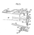
- the rotating frame 38 carries through a pivot 84, a second arm 82 provided at its free end with a knife 86 and d 'forceps 88.
- the arm 82 is controlled by an electromagnet 90.
- the knife 86 consists of a steel blade whose straight edge allows it cutting the wires 10 after they have been welded to the pads 22.
- the clamp 88 is made of a preformed elastic wire, such as a piano cord, folded in the shape of a U to define the jaws 92 of the clamp by its two ends, the elastic wire being fixed to the arm 82 in its middle part by a screw 94.
- the free end of the arm 82 also rigidly carries two fingers 96 defining between them a slot 98 in which the jaws 92 of the clamp 88 are received.
- the fingers 96 cooperate with cam surfaces defined on the edges opposite jaws 92. These cam surfaces are obtained by the fact that the ends of the wire defining the clamp 88 are bent in the shape of a diamond.
- the forceps are open when the fingers 96 are in the vicinity of the acute angle of the rhombus defined by the jaws opposite the end of the forceps 88, and the latter then protrudes beyond the edge of the knife 86 , as shown in FIG. 5.
- the clamp 88 is closed when its end is substantially aligned with the edge of the knife 86, because the fingers 96 then cooperate with the jaws 92 in the vicinity of the obtuse angles of the rhombus defined by the latter and on the side of the end of the pliers.
- the clamp when the clamp is closed, its opening can only be obtained by means of a stop 100 defined on the soldering iron 64 and capable of coming to engage a corresponding stop 102 defined on the upper part of the clamp 88 considering FIG. 5.
- the coming into contact of the stops 100 and 102 makes it possible in fact to bias the jaws 92 downwardly relative to the knife 86 in their open position towards which the clamp 88 is biased by the natural elasticity of the wire which constitutes it.
- the end of the arm 82 also carries a stop 104 against which the clamp 88 comes to bear in the open position, as well as a guide 106.
- the device for making the interconnections of an electrical circuit on an insulating base support which has just been described with reference to Figures 3 to 5 operates as follows.
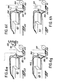
- FIG. 6a illustrates the position occupied by the arm 82 of the device 32 after an interconnection has been made by means of the wire 10 between two pellets 22.
- the caster 58 is raised to the right of the pad after which the wire must be cut ; thus, the wire is not stuck in the cutting zone and its inclination facilitates its gripping by the clamp 88.
- the clamp 88 is then opened as shown in FIG. 5 and its end projects beyond the edge of the knife 86
- the arm 82 then swings around the pivot 84 under the action of the electromagnet 90, as illustrated in FIG. 6b, so that the free end of the clamp 88 comes from first in abutment against the support 14.
- the arm 82 continues to tilt until the edge of the knife 86 cuts the wire 10, so that the fingers 96, rigidly fixed to the knife 86, move down relative to the jaws 92 of the clamp, 88 as successively illustrated in FIGS. 6b and 6c.
- the ends of the jaws 92 are therefore close enough to one another to grasp the non-welded end of the wire 10 when the latter has just been cut by the knife 86.
- the clamp 88 is kept in the tight position, despite the elasticity of the wire which constitutes it, by the fact that the fingers 96 are then situated slightly below the obtuse angles defined by the rhombus formed by the jaws 92 as illustrated in FIG. 6c.
- connection which has just been made by means of the wire 10 is then completely finished and the free end of the latter is tightened by means of the clamp 88, which allows it to be brought to another conductive pad 22 such as the 'illustrates Figure 6d.
- the displacement of the tool head 32 relative to the support in a plane parallel to the latter can be obtained either by displacement of the table 60, or by displacement of the tool head 32, or by combined displacement of these two elements.
- the translational movements are carried out by means of the table 60, and the rotational movements are carried out by means of the pivoting head 32.
- FIG. 6d illustrates the position in which the wire is located just before the creation of a new interconnection between two pads 22.
- the end of the wire 10 is then placed on the welding zone 28 of the corresponding pad 22 and the tip 64 of the soldering iron is located vertically just above this welding zone, the wire 10 being held in this position by means of the clamp 88.
- the fluxing device is then brought into operation. work, that is to say that the arm 66 traverses the path re-represented in dashed lines in FIG.
- the stripping and the actual welding can then be carried out by lowering the tip 64 of the iron until it comes in. contact with the wire 10 still maintained by the clamp 88.
- the heat produced by the tensioning of the soldering iron is communicated almost instantaneously to the entire outer surface of the wire 10 and on the soldering area of the patch 22, so that the heating time makes it possible both to sublimate the layer of polyurethane varnish on the surface of the wire 10 and to weld the wire thus stripped on the zone of solder by fusion of the tin-lead layer being on the surface of this one is very appreciably reduced compared to the known prior processes.
- the components such as the housing 16 are not yet mounted.
- the holes 20 necessary for the passage of the tabs 18 of these components are therefore not blocked, so that the tin risks running into these holes during the soldering phase. This risk is accentuated by the small size of the pellets 22 authorized by the invention. It is however avoided in the patch shown in FIG. 2, by producing a thermal resistance between the welding zone 28 and the connection pad 24, by means of the triangular notches 30. This thermal resistance also makes it possible to maintain the wire on the welding zone 28 when the weld has to undergo reflow, and particularly during a "wave" weld.
- solder is used when the circuit, once wired and soldered by the machine, is then fitted with components (cases for example) to solder these components to the circuit.
- the legs of these components are then soldered to tin in the holes of the pellets, collectively, by "licking one side of the card (the face opposite to the components) by a wave of molten tin-lead.” This is how the soldering of the wires can be remelted, and the wires must therefore remain in place.
- the relatively short duration of heating is determined not by an extremely rapid mechanical operation of the soldering iron, but by an extremely brief energization of. this one.
- Id fer 64 is maintained in the low position shown in FIG. 6f, in which the stop 100 formed on the soldering iron is flush with the stop 102 formed on the clamp 88.
- the opening of the clamp 88 is then obtained by maintaining the iron 64 in its low position while moving the arm 82 upwards as illustrated in FIG. 6g.
- the relative displacement between the clamp 88 and the free end of the arm 82 which results from the abutment of the stop 102 against the stop 100 causes the clamp 88 to open, which then returns to the position shown in FIG. 5.
- the tip 64 of the soldering iron is then reassembled as illustrated in FIG. 6h and another welding can be undertaken in the manner which has just been described, by bringing the tool-holder head 32 opposite. another pad 22 in order to complete the electrical interconnection, the first welding of which has just been described.
- all of the operations are preferably automatic, the machine comprising a control program delivered by a computer.
Landscapes
- Engineering & Computer Science (AREA)
- Manufacturing & Machinery (AREA)
- Microelectronics & Electronic Packaging (AREA)
- Electric Connection Of Electric Components To Printed Circuits (AREA)
- Manufacturing Of Electrical Connectors (AREA)
- Manufacturing Of Printed Wiring (AREA)
Applications Claiming Priority (2)
| Application Number | Priority Date | Filing Date | Title |
|---|---|---|---|
| FR7914592 | 1979-06-07 | ||
| FR7914592A FR2458978A2 (fr) | 1979-06-07 | 1979-06-07 | Procede et dispositif d'interconnexions de composants electronique |
Publications (2)
| Publication Number | Publication Date |
|---|---|
| EP0021894A1 EP0021894A1 (fr) | 1981-01-07 |
| EP0021894B1 true EP0021894B1 (fr) | 1984-10-17 |
Family
ID=9226334
Family Applications (1)
| Application Number | Title | Priority Date | Filing Date |
|---|---|---|---|
| EP80400764A Expired EP0021894B1 (fr) | 1979-06-07 | 1980-05-29 | Procédé et dispositif d'interconnexions de composants électroniques |
Country Status (6)
| Country | Link |
|---|---|
| US (1) | US4337573A (show.php) |
| EP (1) | EP0021894B1 (show.php) |
| JP (1) | JPS5649595A (show.php) |
| CA (1) | CA1179837A (show.php) |
| DE (1) | DE3069451D1 (show.php) |
| FR (1) | FR2458978A2 (show.php) |
Families Citing this family (15)
| Publication number | Priority date | Publication date | Assignee | Title |
|---|---|---|---|---|
| DE3126109A1 (de) * | 1981-07-02 | 1983-01-20 | Vladimir Semenovič Saratov Borisov | Einrichtung zur montage eines drahtes auf einer platte |
| US4450623A (en) * | 1981-12-18 | 1984-05-29 | Kollmorgen Technologies Corporation | Process for the manufacture of circuit boards |
| JPS60795A (ja) * | 1983-06-15 | 1985-01-05 | 東レエンジニアリング株式会社 | 基板回路の結線装置 |
| US4627162A (en) * | 1983-11-04 | 1986-12-09 | Augat Incorporated | Method of producing a wired circuit board |
| US4859807A (en) * | 1985-07-19 | 1989-08-22 | Kollmorgen Technologies Corporation | Wire scribed circuit boards and method of manufacture |
| US4711026A (en) * | 1985-07-19 | 1987-12-08 | Kollmorgen Technologies Corporation | Method of making wires scribed circuit boards |
| US4693778A (en) * | 1985-07-19 | 1987-09-15 | Kollmorgen Technologies Corporation | Apparatus for making scribed circuit boards and circuit board modifications |
| US4864723A (en) * | 1986-07-01 | 1989-09-12 | Preleg, Inc. | Electrical circuit modification method |
| USH487H (en) | 1986-07-14 | 1988-07-05 | The United States Of America As Represented By The Secretary Of The Air Force | Direct cable attach method |
| US5193189A (en) * | 1987-10-07 | 1993-03-09 | Allen-Bradley Company, Inc. | Programmable controller with multiple priority level task processing |
| JPH0691360B2 (ja) * | 1987-12-11 | 1994-11-14 | 株式会社日立製作所 | 細線成形方法 |
| US4948030A (en) * | 1989-01-30 | 1990-08-14 | Motorola, Inc. | Bond connection for components |
| US4987678A (en) * | 1989-03-21 | 1991-01-29 | Harris Corporation | Apparatus for installing wire in grid support structure |
| WO2010149172A2 (en) | 2009-06-24 | 2010-12-29 | Rigshospitalet | SYSTEMIC PRO-HEMOSTATIC EFFECT OF CLOTTING FACTORS IN COMBINATION WITH SYMPATHICOMIMETICS WITH AGONISTIC EFFECTS ON α-ADRENERGIC AND/OR β-ADRENERGIC RECEPTORS OF THE SYMPATHETIC NERVOUS SYSTEM, RELATED TO IMPROVED CLOT STRENGTH. |
| KR102859474B1 (ko) * | 2020-07-10 | 2025-09-15 | 삼성전자주식회사 | 와이어 본딩 장치 |
Family Cites Families (14)
| Publication number | Priority date | Publication date | Assignee | Title |
|---|---|---|---|---|
| US3492389A (en) * | 1968-04-26 | 1970-01-27 | Avisun Corp | Technique for producing synthetic bulk yarns |
| US3500290A (en) * | 1968-07-01 | 1970-03-10 | Beckman Instruments Inc | Terminal construction for electrical circuit element |
| US3812581A (en) * | 1969-11-24 | 1974-05-28 | Wells Electronics | Method for forming electrical joints between intermediate parts of an elongated conductor and selected conductive elements on an electrical assembly |
| US3675840A (en) * | 1969-12-15 | 1972-07-11 | Computer Ind Inc | Wire cutting apparatus for reflow wiring machines |
| US3842190A (en) * | 1969-12-15 | 1974-10-15 | Computer Ind Inc | Wire routing system |
| JPS5550399B1 (show.php) * | 1970-03-05 | 1980-12-17 | ||
| US3643321A (en) * | 1970-06-17 | 1972-02-22 | Kulicke & Soffa Ind Inc | Method and apparatus for tailless wire bonding |
| FR2191399B3 (show.php) * | 1972-06-28 | 1975-08-29 | Matra Engins | |
| US3786172A (en) * | 1972-12-07 | 1974-01-15 | Accra Point Arrays Corp | Printed circuit board method and apparatus |
| US3960309A (en) * | 1974-07-31 | 1976-06-01 | International Business Machines Corporation | Fine wire twisted pair routing and connecting system |
| JPS5127036A (ja) * | 1974-08-30 | 1976-03-06 | Yokogawa Electric Works Ltd | Deijitarumaruchireberukonpareeta |
| US3981076A (en) * | 1974-11-27 | 1976-09-21 | Commissariat A L'energie Atomique | Method of connecting electronic microcomponents |
| SU605703A1 (ru) * | 1975-11-12 | 1978-05-05 | Рижский Ордена Ленина Государственный Электротехнический Завод Вэф Им. В.И.Ленина | Устройство дл флюсовани , пайки и лужени волной |
| US4031612A (en) * | 1976-03-02 | 1977-06-28 | Commissariat A L'energie Atomique | Method and a device for the interconnection of electronic components |
-
1979
- 1979-06-07 FR FR7914592A patent/FR2458978A2/fr active Granted
-
1980
- 1980-05-29 EP EP80400764A patent/EP0021894B1/fr not_active Expired
- 1980-05-29 US US06/154,144 patent/US4337573A/en not_active Expired - Lifetime
- 1980-05-29 DE DE8080400764T patent/DE3069451D1/de not_active Expired
- 1980-06-04 CA CA000353565A patent/CA1179837A/en not_active Expired
- 1980-06-06 JP JP7707080A patent/JPS5649595A/ja active Pending
Also Published As
| Publication number | Publication date |
|---|---|
| CA1179837A (en) | 1984-12-27 |
| FR2458978A2 (fr) | 1981-01-02 |
| DE3069451D1 (en) | 1984-11-22 |
| US4337573A (en) | 1982-07-06 |
| JPS5649595A (en) | 1981-05-06 |
| FR2458978B2 (show.php) | 1981-10-23 |
| EP0021894A1 (fr) | 1981-01-07 |
Similar Documents
| Publication | Publication Date | Title |
|---|---|---|
| EP0021894B1 (fr) | Procédé et dispositif d'interconnexions de composants électroniques | |
| EP1992018B1 (fr) | Procede de couplage de cellules photovoltaiques et film permettant sa mise en oeuvre | |
| EP0121467B1 (fr) | Microconnecteur à haute densité de contacts | |
| JPH036867A (ja) | 光発電素子の電極構造、形成方法、及びその製造装置 | |
| FR2598584A1 (fr) | Dispositif de fabrication de plaquettes a circuits traces | |
| EP1160937B1 (fr) | Elément de raccordement électrique soudable avec dépôt de soudure | |
| FR2759616A1 (fr) | Appareil d'empilage et de brasage automatise pour dispositifs de modules empiles tridimensionnels et procede de fabrication de celui-ci | |
| EP0589748A1 (fr) | Procédé pour permettre le montage d'une puce sur un substrat, et puce préparée selon le procédé | |
| WO1998044478A1 (fr) | Ecran et montage des circuits de commande des pixels de l'ecran | |
| FR2728392A1 (fr) | Procede et support de connexion d'un circuit integre a un autre support par l'intermediaire de boules | |
| EP1133010A1 (fr) | Pièce de contact pour connecteur éléctrique | |
| FR2489611A1 (fr) | Procede de fabrication d'un support d'affichage pour diode electroluminescente | |
| EP0312415A1 (fr) | Plaque circuit pour courants élevés et procédé de préparation | |
| EP0334709B1 (fr) | Appareil d'étamage sélectif des conducteurs d'un support de circuit intégré de haute densité et procédé d'étamage utilisant un tel appareil | |
| CH665074A5 (fr) | Procede de soudage d'un composant electrique a un ensemble de pattes de connexion ainsi que machine et ruban pour la mise en oeuvre de ce procede. | |
| EP0083265B1 (fr) | Support d'interconnexion d'un boîtier de circuit intégré sur un circuit imprimé, et système d'interconnexion utilisant un tel support | |
| EP0178977A1 (fr) | Composant semiconducteur monté en boîtier plastique, et procédé de montage correspondant | |
| EP0624921B1 (fr) | Dispositif de raccordement électrique et procédé de fabrication correspondant | |
| FR2526624A1 (fr) | Procede de soudage a grande vitesse pour cablage | |
| EP0242667B1 (fr) | Outil de soudage pour dispositifs électroniques | |
| EP1333481B1 (fr) | Procédé de soudage de conducteurs sur des substrats | |
| EP0043778A1 (fr) | Procédé et appareil de présoudage de billes de soudure sur des pattes de connexion | |
| FR2565425A1 (fr) | Procede pour la fabrication de boites de distribution electrique | |
| FR2571547A1 (fr) | Circuit hybride reportable sur un support comportant un reseau d'interconnexion a haute densite | |
| JPH0622425A (ja) | 電線被覆むき補助器 |
Legal Events
| Date | Code | Title | Description |
|---|---|---|---|
| PUAI | Public reference made under article 153(3) epc to a published international application that has entered the european phase |
Free format text: ORIGINAL CODE: 0009012 |
|
| AK | Designated contracting states |
Designated state(s): CH DE GB IT |
|
| 17P | Request for examination filed |
Effective date: 19810603 |
|
| ITF | It: translation for a ep patent filed | ||
| GRAA | (expected) grant |
Free format text: ORIGINAL CODE: 0009210 |
|
| AK | Designated contracting states |
Designated state(s): CH DE GB IT LI |
|
| REF | Corresponds to: |
Ref document number: 3069451 Country of ref document: DE Date of ref document: 19841122 |
|
| PLBE | No opposition filed within time limit |
Free format text: ORIGINAL CODE: 0009261 |
|
| STAA | Information on the status of an ep patent application or granted ep patent |
Free format text: STATUS: NO OPPOSITION FILED WITHIN TIME LIMIT |
|
| 26N | No opposition filed | ||
| PG25 | Lapsed in a contracting state [announced via postgrant information from national office to epo] |
Ref country code: GB Effective date: 19880529 |
|
| PG25 | Lapsed in a contracting state [announced via postgrant information from national office to epo] |
Ref country code: LI Effective date: 19880531 Ref country code: CH Effective date: 19880531 |
|
| REG | Reference to a national code |
Ref country code: CH Ref legal event code: PL |
|
| GBPC | Gb: european patent ceased through non-payment of renewal fee | ||
| PG25 | Lapsed in a contracting state [announced via postgrant information from national office to epo] |
Ref country code: DE Effective date: 19890201 |