EP0020746B1 - Process and apparatus for cleaning wall deposits from a film deposition furnace tube - Google Patents
Process and apparatus for cleaning wall deposits from a film deposition furnace tube Download PDFInfo
- Publication number
- EP0020746B1 EP0020746B1 EP19800900181 EP80900181A EP0020746B1 EP 0020746 B1 EP0020746 B1 EP 0020746B1 EP 19800900181 EP19800900181 EP 19800900181 EP 80900181 A EP80900181 A EP 80900181A EP 0020746 B1 EP0020746 B1 EP 0020746B1
- Authority
- EP
- European Patent Office
- Prior art keywords
- tube
- furnace
- plasma
- deposit
- gas
- Prior art date
- Legal status (The legal status is an assumption and is not a legal conclusion. Google has not performed a legal analysis and makes no representation as to the accuracy of the status listed.)
- Expired
Links
- 230000008021 deposition Effects 0.000 title claims abstract description 47
- 238000004140 cleaning Methods 0.000 title claims abstract description 39
- 238000000034 method Methods 0.000 title claims abstract description 28
- 230000008569 process Effects 0.000 title claims abstract description 23
- 238000005530 etching Methods 0.000 claims abstract description 34
- 230000008878 coupling Effects 0.000 claims abstract description 14
- 238000010168 coupling process Methods 0.000 claims abstract description 14
- 238000005859 coupling reaction Methods 0.000 claims abstract description 14
- 238000011065 in-situ storage Methods 0.000 claims abstract description 10
- 239000007789 gas Substances 0.000 claims description 41
- HQVNEWCFYHHQES-UHFFFAOYSA-N silicon nitride Chemical group N12[Si]34N5[Si]62N3[Si]51N64 HQVNEWCFYHHQES-UHFFFAOYSA-N 0.000 claims description 25
- 229910052581 Si3N4 Inorganic materials 0.000 claims description 24
- VYPSYNLAJGMNEJ-UHFFFAOYSA-N Silicium dioxide Chemical compound O=[Si]=O VYPSYNLAJGMNEJ-UHFFFAOYSA-N 0.000 claims description 13
- XUIMIQQOPSSXEZ-UHFFFAOYSA-N Silicon Chemical compound [Si] XUIMIQQOPSSXEZ-UHFFFAOYSA-N 0.000 claims description 12
- 229910052710 silicon Inorganic materials 0.000 claims description 12
- 239000010703 silicon Substances 0.000 claims description 12
- 239000000376 reactant Substances 0.000 claims description 11
- 238000010438 heat treatment Methods 0.000 claims description 9
- 229910052814 silicon oxide Inorganic materials 0.000 claims description 7
- 230000005684 electric field Effects 0.000 claims description 5
- QVGXLLKOCUKJST-UHFFFAOYSA-N atomic oxygen Chemical compound [O] QVGXLLKOCUKJST-UHFFFAOYSA-N 0.000 claims description 4
- QSHDDOUJBYECFT-UHFFFAOYSA-N mercury Chemical compound [Hg] QSHDDOUJBYECFT-UHFFFAOYSA-N 0.000 claims description 4
- 229910052753 mercury Inorganic materials 0.000 claims description 4
- 239000001301 oxygen Substances 0.000 claims description 4
- 229910052760 oxygen Inorganic materials 0.000 claims description 4
- 239000003990 capacitor Substances 0.000 claims description 3
- 239000004020 conductor Substances 0.000 claims description 2
- 239000000758 substrate Substances 0.000 claims description 2
- IIGJROFZMAKYMN-UHFFFAOYSA-N [C].FC(F)(F)F Chemical compound [C].FC(F)(F)F IIGJROFZMAKYMN-UHFFFAOYSA-N 0.000 claims 1
- 239000000126 substance Substances 0.000 abstract description 2
- 238000000151 deposition Methods 0.000 description 48
- 235000012431 wafers Nutrition 0.000 description 21
- QGZKDVFQNNGYKY-UHFFFAOYSA-N Ammonia Chemical compound N QGZKDVFQNNGYKY-UHFFFAOYSA-N 0.000 description 7
- IJGRMHOSHXDMSA-UHFFFAOYSA-N Atomic nitrogen Chemical compound N#N IJGRMHOSHXDMSA-UHFFFAOYSA-N 0.000 description 4
- 150000008282 halocarbons Chemical class 0.000 description 4
- 239000000463 material Substances 0.000 description 4
- 150000004767 nitrides Chemical class 0.000 description 4
- 229910021529 ammonia Inorganic materials 0.000 description 3
- 238000005229 chemical vapour deposition Methods 0.000 description 3
- 230000001276 controlling effect Effects 0.000 description 3
- 235000012239 silicon dioxide Nutrition 0.000 description 3
- TXEYQDLBPFQVAA-UHFFFAOYSA-N tetrafluoromethane Chemical compound FC(F)(F)F TXEYQDLBPFQVAA-UHFFFAOYSA-N 0.000 description 3
- 238000011144 upstream manufacturing Methods 0.000 description 3
- KRHYYFGTRYWZRS-UHFFFAOYSA-N Fluorane Chemical compound F KRHYYFGTRYWZRS-UHFFFAOYSA-N 0.000 description 2
- VEXZGXHMUGYJMC-UHFFFAOYSA-N Hydrochloric acid Chemical compound Cl VEXZGXHMUGYJMC-UHFFFAOYSA-N 0.000 description 2
- 229910052799 carbon Inorganic materials 0.000 description 2
- 239000000356 contaminant Substances 0.000 description 2
- 230000003247 decreasing effect Effects 0.000 description 2
- MROCJMGDEKINLD-UHFFFAOYSA-N dichlorosilane Chemical compound Cl[SiH2]Cl MROCJMGDEKINLD-UHFFFAOYSA-N 0.000 description 2
- 239000005350 fused silica glass Substances 0.000 description 2
- 230000006698 induction Effects 0.000 description 2
- 230000001939 inductive effect Effects 0.000 description 2
- 239000000203 mixture Substances 0.000 description 2
- 229910052757 nitrogen Inorganic materials 0.000 description 2
- 239000002245 particle Substances 0.000 description 2
- BASFCYQUMIYNBI-UHFFFAOYSA-N platinum Chemical compound [Pt] BASFCYQUMIYNBI-UHFFFAOYSA-N 0.000 description 2
- 239000010453 quartz Substances 0.000 description 2
- XLYOFNOQVPJJNP-UHFFFAOYSA-N water Substances O XLYOFNOQVPJJNP-UHFFFAOYSA-N 0.000 description 2
- OKTJSMMVPCPJKN-UHFFFAOYSA-N Carbon Chemical compound [C] OKTJSMMVPCPJKN-UHFFFAOYSA-N 0.000 description 1
- PXGOKWXKJXAPGV-UHFFFAOYSA-N Fluorine Chemical compound FF PXGOKWXKJXAPGV-UHFFFAOYSA-N 0.000 description 1
- ZOKXTWBITQBERF-UHFFFAOYSA-N Molybdenum Chemical compound [Mo] ZOKXTWBITQBERF-UHFFFAOYSA-N 0.000 description 1
- GRYLNZFGIOXLOG-UHFFFAOYSA-N Nitric acid Chemical class O[N+]([O-])=O GRYLNZFGIOXLOG-UHFFFAOYSA-N 0.000 description 1
- 239000002253 acid Substances 0.000 description 1
- 230000009471 action Effects 0.000 description 1
- 230000008859 change Effects 0.000 description 1
- 239000011538 cleaning material Substances 0.000 description 1
- 239000000470 constituent Substances 0.000 description 1
- 238000005336 cracking Methods 0.000 description 1
- 230000007547 defect Effects 0.000 description 1
- 230000000593 degrading effect Effects 0.000 description 1
- 238000001035 drying Methods 0.000 description 1
- 230000000694 effects Effects 0.000 description 1
- 238000005516 engineering process Methods 0.000 description 1
- 229910052731 fluorine Inorganic materials 0.000 description 1
- 239000011737 fluorine Substances 0.000 description 1
- PCHJSUWPFVWCPO-UHFFFAOYSA-N gold Chemical compound [Au] PCHJSUWPFVWCPO-UHFFFAOYSA-N 0.000 description 1
- 229910052737 gold Inorganic materials 0.000 description 1
- 239000010931 gold Substances 0.000 description 1
- 239000001257 hydrogen Substances 0.000 description 1
- 229910052739 hydrogen Inorganic materials 0.000 description 1
- 125000004435 hydrogen atom Chemical class [H]* 0.000 description 1
- 230000006872 improvement Effects 0.000 description 1
- 239000011261 inert gas Substances 0.000 description 1
- 238000007689 inspection Methods 0.000 description 1
- 238000004519 manufacturing process Methods 0.000 description 1
- 238000002844 melting Methods 0.000 description 1
- 229910052750 molybdenum Inorganic materials 0.000 description 1
- 239000011733 molybdenum Substances 0.000 description 1
- 229910000069 nitrogen hydride Inorganic materials 0.000 description 1
- 230000009972 noncorrosive effect Effects 0.000 description 1
- 231100000252 nontoxic Toxicity 0.000 description 1
- 230000003000 nontoxic effect Effects 0.000 description 1
- 239000007800 oxidant agent Substances 0.000 description 1
- 230000001590 oxidative effect Effects 0.000 description 1
- 229920002120 photoresistant polymer Polymers 0.000 description 1
- 238000001020 plasma etching Methods 0.000 description 1
- 229910052697 platinum Inorganic materials 0.000 description 1
- 229920000642 polymer Polymers 0.000 description 1
- 239000000843 powder Substances 0.000 description 1
- 230000009467 reduction Effects 0.000 description 1
- 230000001105 regulatory effect Effects 0.000 description 1
- 239000004065 semiconductor Substances 0.000 description 1
- 238000005389 semiconductor device fabrication Methods 0.000 description 1
- 239000000377 silicon dioxide Substances 0.000 description 1
- 229910052715 tantalum Inorganic materials 0.000 description 1
- GUVRBAGPIYLISA-UHFFFAOYSA-N tantalum atom Chemical compound [Ta] GUVRBAGPIYLISA-UHFFFAOYSA-N 0.000 description 1
- MZLGASXMSKOWSE-UHFFFAOYSA-N tantalum nitride Chemical compound [Ta]#N MZLGASXMSKOWSE-UHFFFAOYSA-N 0.000 description 1
- WFKWXMTUELFFGS-UHFFFAOYSA-N tungsten Chemical compound [W] WFKWXMTUELFFGS-UHFFFAOYSA-N 0.000 description 1
- 229910052721 tungsten Inorganic materials 0.000 description 1
- 239000010937 tungsten Substances 0.000 description 1
- 230000000007 visual effect Effects 0.000 description 1
- 238000011179 visual inspection Methods 0.000 description 1
Images

Classifications
-
- H—ELECTRICITY
- H01—ELECTRIC ELEMENTS
- H01J—ELECTRIC DISCHARGE TUBES OR DISCHARGE LAMPS
- H01J37/00—Discharge tubes with provision for introducing objects or material to be exposed to the discharge, e.g. for the purpose of examination or processing thereof
- H01J37/32—Gas-filled discharge tubes
- H01J37/32431—Constructional details of the reactor
- H01J37/32798—Further details of plasma apparatus not provided for in groups H01J37/3244 - H01J37/32788; special provisions for cleaning or maintenance of the apparatus
- H01J37/32853—Hygiene
- H01J37/32862—In situ cleaning of vessels and/or internal parts
-
- C—CHEMISTRY; METALLURGY
- C23—COATING METALLIC MATERIAL; COATING MATERIAL WITH METALLIC MATERIAL; CHEMICAL SURFACE TREATMENT; DIFFUSION TREATMENT OF METALLIC MATERIAL; COATING BY VACUUM EVAPORATION, BY SPUTTERING, BY ION IMPLANTATION OR BY CHEMICAL VAPOUR DEPOSITION, IN GENERAL; INHIBITING CORROSION OF METALLIC MATERIAL OR INCRUSTATION IN GENERAL
- C23C—COATING METALLIC MATERIAL; COATING MATERIAL WITH METALLIC MATERIAL; SURFACE TREATMENT OF METALLIC MATERIAL BY DIFFUSION INTO THE SURFACE, BY CHEMICAL CONVERSION OR SUBSTITUTION; COATING BY VACUUM EVAPORATION, BY SPUTTERING, BY ION IMPLANTATION OR BY CHEMICAL VAPOUR DEPOSITION, IN GENERAL
- C23C16/00—Chemical coating by decomposition of gaseous compounds, without leaving reaction products of surface material in the coating, i.e. chemical vapour deposition [CVD] processes
- C23C16/44—Chemical coating by decomposition of gaseous compounds, without leaving reaction products of surface material in the coating, i.e. chemical vapour deposition [CVD] processes characterised by the method of coating
- C23C16/4401—Means for minimising impurities, e.g. dust, moisture or residual gas, in the reaction chamber
- C23C16/4405—Cleaning of reactor or parts inside the reactor by using reactive gases
-
- H—ELECTRICITY
- H01—ELECTRIC ELEMENTS
- H01J—ELECTRIC DISCHARGE TUBES OR DISCHARGE LAMPS
- H01J37/00—Discharge tubes with provision for introducing objects or material to be exposed to the discharge, e.g. for the purpose of examination or processing thereof
- H01J37/32—Gas-filled discharge tubes
- H01J37/32009—Arrangements for generation of plasma specially adapted for examination or treatment of objects, e.g. plasma sources
- H01J37/32082—Radio frequency generated discharge
- H01J37/321—Radio frequency generated discharge the radio frequency energy being inductively coupled to the plasma
Definitions
- the invention relates to the cleaning of deposition systems and, more particularly, to cleaning furnace tubes used for chemical vapor deposition of films such as silicon (both polycrystalline and monocrystalline), silicon oxide and silicon nitride.
- Silicon, silicon oxide and silicon nitride films are widely used in miroelectronics technology. Their deposition can be by any one of a number of processes including plasma deposition, chemical vapor deposition, etc.
- Low pressure, chemical vapor deposition (LPCVD) using large-tube furnaces combines the deposition control and quality which is characteristic of CVD processes with the ability to process large wafer loads.
- LPCVD chemical vapor deposition
- the interior wall(s) of the furnace tube becomes (become) coated with the film constituents and other contaminants. The result is flaking of the deposit or cracking of the tube due to the different thermal expansions of the tube material, usually quartz, and the deposit.
- a powder is frequently deposited in the cooler regions of the tube such as at the loading door at the entrance to the tube.
- Deposits such as these are a source of particulates which alter the deposition rate and contaminate the deposited film, and cause defects in the form of pinholes, granular surface regions, etc.
- the furnace tube must be cleaned periodically. Cleaning typically involves allowing the tube to cool; removing the tube from the furnace; cleaning the tube by etching for several hours in a wet bath containing, e.g., a 1:1 ratio by volume of concentrated hydrofluoric and nitric acids; rinsing the tube in water; replacing the tube; and resetting the deposition temperature cycle, which is perturbed when the tube is removed. After replacing the tube, the furnace is heated to 100°C or higher to vaporize any remaining water. This cleaning process is time- consuming and involves the risks of tube breakage and handling corrosive cleaning materials.
- Plasma furnaces or CVD reactor furnaces have been used to perform different operations in the reactor by altering the reactor atmosphere.
- U.S. 3,940,506 issued February 24, 1976 to Heinecke teaches etching silicon dioxide or depositing a polymer by controlling the concentration of reducing species, such as hydrogen, in a plasma etchant which contains fluorine and carbon.
- U.S. 3,867,216 issued February 18, 1975 to Jacob teaches etching oxide or nitride without degrading a photoresist mask, and then stripping the mask, by varying the oxygen ratio in a plasma- forming binary mixture of oxygen and halocarbon.
- U.S. 3,945,846 issued March 23, 1976 to Goldsmith et al uses the same reactor furnace to etch silicon and hydrochloric acid, then deposit epitaxial silicon by the reduction of dichlorosilane, both at 1,050°C. to 1,200°C.
- U.S. 3,914,127 issued October 21, 1975 to Buss et al teaches the use of a plasma reactor to perform several of the steps of fabricating a CCD device, including sequentially etching an oxide or nitride film in a plasma-containing carbon tetrafluoride at less than 150°C, then depositing oxide or nitride from a plasma at 200°C to 400°C.
- a process for cleaning wall deposits from a furnace tube used in a film deposition furnace system the tube having a gas inlet end and a gas exit end, the improvement wherein the tube is cleaned in situ in the furnace, comprising: maintaining the tube interior at subatmospheric pressure; supplying gas to the gas inlet end of the tube, the gas being suitable for creating a deposit-etching plasma; generating RF energy; and applying the RF energy to RF element means located along a selected portion of the tube adjacent the gas inlet end for coupling the RF energy to the gas to form a deposit-etching plasma over at least the selected portion of the tube.
- the cleaning of a furnace tube without its removal from the furnace reduces operating time and costs and increases safety of operation. Also, the use of plasma cleaning is advantageous, since plasma is economical, low in contaminants, non-toxic and non-corrosive.
- the invention may be used to clean dielectric films such as silicon oxide and silicon nitride, conductor films, and semiconductor films such as silicon.
- the cleaning plasma can be extended outside the selected portion of the tube occupied by the RF element by decreasing the reactant flow rate, decreasing the pressure, and/or varying the power.
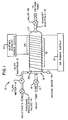
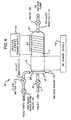
- Figs. 1-4 are schematic representations of alternative embodiments of LPCVD systems which have in situ, plasma self-cleaning capability.
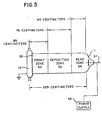
- Fig. 5 is a cross-sectional representation of the furnace tube used in practicing the invention, showing zone dimensions and means for applying an electric field to the furnace tube.
- Fig. 1 is a schematic illustration of one embodiment of apparatus 10 for both depositing films such as silicon nitride using LPCVD, and also for cleaning the furnace tube(s) in which deposition takes place, in situ, using a plasma etch.
- the apparatus 10 comprises an LPCVD furnace system including a tube 11, typically made of fused quartz, having a cover 12 at the inlet end 26 of the tube and a gas inlet manifold 13. Gaseous reactants are admitted to the tube 11 via the inlet manifold 13 and flow rates are controlled by a pressure-regulating valve 14 and read from a flow meter 16, both of which are connected to the inlet manifold. Gas inlet 17, which is opened and closed by valve 18, connects the interior of the tube 11 to a source of inert gas, such as nitrogen. Vacuum gauge 19 is connected to the interior of the tube adjacent the inlet end 26 for providing readings of the internal pressure.
- a source of inert gas such as nitrogen.
- Vacuum gauge 19 is connected to the interior of the tube adjacent the inlet end 26 for providing readings of the internal pressure.
- the opposite, exhaust end 27 of the tube is connected to an exhaust manifold 21, to which is connected a gate valve 22 for controlling the connection of the tube 11 to a vacuum pump (not shown).
- the path of movement of gases along the tube is from the inlet end 26 to the exhaust end 27.
- downstream or upstream refer to this flow.
- a power supply 23 provides current to electric resistance heating coils 24 for heating the internal volume of the tube 11 and for pyrolytically depositing silicon, silicon nitride, silicon oxide or other films from the reactants entering via inlet manifold 13.
- FIG. 1 An example of a furnace system which employs the type of arrangement shown in Fig. 1 is the model 4000S-72.00, available from Thermco Products Corp., 1465 No. Batavia St., Orange, California 92668.
- This furnace system contains four interchangeable furnace tubes 11, which are supplied, heated and evacuated as shown in Fig. 1.
- the tubes typically are about 229 centimeters long and about 13.5 centimeters in diameter. Each tube can hold approximately 120 10.2 centimeters diameter wafers.
- the heating rods 24 span approximately the 178-191 centimeters of tube length adjacent the exit end 27. This length is sufficient to provide reproducible deposition along the length of the deposition zone.
- deposition zone 52 is an approximately 76 centimeter long central region having a closely controlled temperature profile. The deposition zone is flanked by cooler, front and rear zones 53 and 54.
- an RF plasma-generating element (or elements) is (are) provided along a selected length of the tube to provide a plasma for cleaning the aforementioned deposit from at least the selected length.
- RF energy is supplied by a power supply 31 and the RF energy is coupled to the tube 11 by an RF element in the form of an induction coil 32 which surrounds the tube and extends along substantially the length of the tube.
- the RF energy generates an etching plasma when suitable reactants, typically a halocarbon and an oxidant, are admitted via inlet manifold 13.
- the reactant gas, reactant gas flow rate, RF power, and internal pressure control the removal rate or etch rate provided by the plasma.
- the type of reactant gas can be selected- such as by selecting the type of halocarbon (freon) and the ratio of halocarbon to oxygen- to provide the optimum etch rates for different films.
- the RF heating element is not limited to an induction coil 32.
- the RF heating element is a pair of capacitor plates 33-33 which capacitively couple RF power from supply 34 to the tube 11.
- the plates 33-33 can be of platinum or tungsten or other high-melting point material which is plated, painted or otherwise applied to the tube 11.
- plates 33-33 can be mounted about the outside of the tube.
- the plate area can be varied along the length of the tube 11 to vary the RF power profile along the tube.
- Capacitive coupling is thought (1) to be accompanied by higher temperatures than is inductive coupling and (2) to create more collisions with the tube walls than does inductive coupling. Both features should provide enhanced cleaning ability.
- plasma-creating energy can be applied to the portion of the furnace tube 11 encompassed by the RF coupling element 24 by coupling the RF power directly to the element.
- RF power supply 36 is coupled to the heating element 24 by matching network 37.
- a separate RF power supply 38 is coupled to RF element 39, which may be a coil (similar to coil 32 of Fig. 1) or capacitive plates (similar to plates 33-33 of Fig. 2), to clean the portion of the tube in front of heating element 24.
- the RF coupling element (coil, plates, etc.) need not span the entire length of the tube in order to clean along the entire length of the tube. Indeed, plasma techniques can be used to clean the entire tube, even if a partial-length RF coupling element encompasses substantially less than the tube length. To accomplish this, and referring to Fig. 4, the partial-length RF coupling element 41 is positioned adjacent the front end 26 of the tube. Then, by controlling the etch parameters, the plasma generated by element 41 and power supply 42 can be extended toward the rear 27 of the tube.
- a DC or AC electric field could be applied by power supply 56 between the grounded door 12 and an electrode 57 inserted in the tube 11 through the exhaust manifold 21. See Fig. 5.
- the charged particles can be accelerated towards the deposition zone by the appropriate selection of flow pressure and applied voltage. The accelerated particles will in turn produce the more active species necessary to etch or aid in etching the walls of the tube. This arrangement would be particularly helpful in etching the rear zone.
- the partial-length RF coupling element 41 is upstream relative to the flow of reactants through the tube 11 in order for the plasma to be extended. That is, positioning the partial-length RF element 41 downstream, proximate the exit end or rear 27 of the tube, would make cleaning the front of the tube more difficult, for the plasma cannot be easily extended upstream.
- the tube 11 was preheated to between 700-850 0 C, and as many as 120 wafers were placed in the approximately 76 centimeter long deposition zone 52 (Fig. 5).
- the cover 12 was then attached, gas inlet tube 17 was closed, and the vacuum pump was used to evacuate the interior of the tube to a pressure of about one micron of mercury.
- Ammonia (NH 3 ) was then supplied to the interior of the tube via inlet manifold 13 at a flow rate of between 50-100 sccpm (standard cubic centimeters per minute).
- Dichlorosilane gas, SiH I C1 2 (DCS) was then added at a flow rate of 10-30 sccpm to the ammonia flow to deposit silicon nitride on the partially- processed wafers.
- these exemplary temperature, flow rate and internal pressure parameters provided an initial silicon nitride deposition rate of about 10 to 50 Angstroms per minute (.001 to .005 microns).
- the above deposition cycle was employed a number of times, each to form 500 Angstrom- thick (0.05 microns thick) silicon nitride films on silicon substrates.
- the initial deposition rate (using a furnace tube which had been cleaned using the above-described wet, hydrofluoric acid:nitride acid etch) was 19 Angstroms (.0019 microns) per minute.
- the tube walls were covered by a silicon nitride-containing deposit that was believed to be about 12,000 Angstroms (1.2 microns) thick.
- This thick deposit (indeed even the much thinner deposit resulting from only a few deposition cycles) is characterized by a change in deposition rate from the 19 Angstroms (.0019 microns) per minute rate (for the clean tube) to 24 Angstroms (.0024 microns) per minute.
- the RF plasma arrangement of Fig. 4 was then applied in an attempt to clean the silicon nitride deposit.
- the RF coil 41 occupied about 25 cm at the front of the approximately 89 centimeter long front zone 53.
- the Thermco furnace provides an approximately 76 cm long, controlled-temperature deposition zone 52 which is flanked by the cooler, 89 centimeter long front zone 53 and 64 centimeter long rear zone 54.
- wafer film deposition is confined within the deposition zone. It is common to observe the build-up of an amorphous, soft yellow film in the front zone.
- Tube cleaning was attempted using the power supply 42 to inductively apply 400 to 500 watts of RF power to the coil 41, and using the inlet manifold 13 and pressure regulating valve 14 to inlet an etching gas comprising approximately four to seventeen percent by volume oxygen and the rest substantially CF 4 into the tube at a flow rate of 1 to 5 sccpm (standard cubic centimeters per minute) as measured by the flow meter 16.
- This gas is available from LFE Corporation, 1601 Trapelo Road, Waltham, Massachusetts under the trade name DE-100).
- the vacuum pump maintained an internal tube pressure of 100 to 150 microns as measured by the vacuum gauge 19.
- a furnace tube 11 was cleaned using the above-described, conventional wet etch bath technique, then the tube was inserted in the furnace and about twenty five 500 Angstroms silicon nitride deposition cycles were performed using the process of Example 1.
- the CF 4 O Z etching gas of Example 1 was inlet at 50 sccpm and at 200 microns pressure, using only 100 watts of RF power. After a 20 minute etch, the quartz wall in the front zone 53 was translucent, indicating the deposited film had been completely removed.
- a silicon wafer having a 444 Angstrom (.0444 micron) thick silicon nitride film thereon was placed at the center of the deposition zone.
- the 100 watts of power, 50 sccpm etchant gas flow rate, and 200 micron pressure parameters were again applied, with the result that approximately 35 Angstroms (.0035 microns) of the silicon nitride film were removed in two minutes.
- Etching was continued, this time using an increased gas flow rate of about 6 sccpm, which resulted in a pressure of 140 microns of mercury.
- the RF power was 400 watts.
- the etch time was 15 minutes. Visual inspection of the deposition zone indicated that this zone was much cleaner than before, although there appeared to be a slight residue.
- Two silicon wafers were first coated with a silicon nitride film.
- the film thickness was 644 Angstroms (.0644 micron) and 498 Angstroms (.0498 micron) for wafer No. 1 and wafer No. 2, respectively.
- the wafers were positioned 25 centimeters apart on a boat which was centered in the deposition zone with the wafers perpendicular to the longitudinal axis of the tube (perpendicular to the direction of flow of the reactants).
- the wafers were etched for 15 minutes using the CF Q 0 2 etching gas at a flow rate of about 6 sccpm, a pressure of 140 microns, and power of 400 watts.
- This etch removed about 266 Angstroms (.0266 micron) and 180 Angstroms (.018 micron) of silicon nitride from the first and second wafers, leaving a remaining thickness of 378 Angstroms (.0378 micron) and 311 Angstroms (.0311 micron), respectively.
- the average etch rate was thus 18 Angstroms (.0018 micron) per minute for wafer No. 1 (which was located nearer the RF coil 41), and 12 Angstroms (.0012 micron) per minute for wafer No. 2.
- plasma etch techniques can be applied to clean deposits such as silicon nitride from large reactor furnace tubes in situ without removing the tube from the furnace.
- a wide range of power, flow rate, and pressure parameters can be applied not only to clean the tube in the vicinity of the coil, but also, by using an RF element spanning the length of the tube (as shown in Fig. 1), to clean along the entire length of the tube.
- silicon, silicon oxide, tantalum, tantalum nitride and molybdenum are rapidly or moderately etched by CF 4 -02 etching gas.
- films and layers of these materials such as films formed on wafers, can be etched, thus presenting the capability of depositing films, etching the films, and cleaning tube deposits in the same furnace system with minimum handling of the furnace tube.
- a film such as silicon, silicon oxide or silicon nitride could be deposited on wafers positioned in the tube 11 within the furnace system, then the wafers would be removed from the tube and masked, and the masked wafers would be reinserted in the tube for simultaneously etching the films and cleaning tube deposits.
- Examples 2-4 demonstrate the ability to extend the effective etching range by varying the etch parameters. Also, Examples 2-4 demonstrate that an RF element spanning about 25 centimeters of the front zone 53 (the front 89 centimeters of the tube) can be used not only to clean the entire front zone, but also to clean the middle, deposition zone 52. Based upon the lower, 12 Angstrom per minute etch rate (0.0012 microns per minute) of Example 4, the 12,000 Angstrom (1.2 micron) deposit would be completely removed from the deposition zone 52 in about 17 hours. This demonstrates that a coil covering no more than 25 centimeters of the front zone 53 can clean more than two-thirds of the tube within this time span.
- the apparatus of Figs. 1-5 would be useful in a portable RF plasma cleaning.
- the capacitive plates 33 could be formed on the tube 11, or formed as a separate unit which is attached to the tube 11, or could be a separate unit which is permanently attached to the furnace.
- a portable RF power source would supply power.
- a vacuum source would be used to provide pressures or perhaps 0.1 to 1 torr to institute a cleaning procedure for several hours or overnight. At the end of the cleaning, the portable RF source would be disconnected from the plates and, perhaps, moved to another furnace for another cleaning cycle.
- RF coupling elements may be placed along the front and rear zones of the tube and the etch parameters controlled so that the effective etching extends between the elements and along the length of the tube.
Landscapes
- Chemical & Material Sciences (AREA)
- Engineering & Computer Science (AREA)
- Physics & Mathematics (AREA)
- Analytical Chemistry (AREA)
- Plasma & Fusion (AREA)
- Materials Engineering (AREA)
- Metallurgy (AREA)
- Organic Chemistry (AREA)
- Health & Medical Sciences (AREA)
- Epidemiology (AREA)
- Public Health (AREA)
- Mechanical Engineering (AREA)
- Chemical Kinetics & Catalysis (AREA)
- General Chemical & Material Sciences (AREA)
- Drying Of Semiconductors (AREA)
- Central Air Conditioning (AREA)
Abstract
Description
- The invention relates to the cleaning of deposition systems and, more particularly, to cleaning furnace tubes used for chemical vapor deposition of films such as silicon (both polycrystalline and monocrystalline), silicon oxide and silicon nitride.
- Silicon, silicon oxide and silicon nitride films are widely used in miroelectronics technology. Their deposition can be by any one of a number of processes including plasma deposition, chemical vapor deposition, etc. Low pressure, chemical vapor deposition (LPCVD) using large-tube furnaces combines the deposition control and quality which is characteristic of CVD processes with the ability to process large wafer loads. However, it is typical that after even a few deposition cycles, the interior wall(s) of the furnace tube becomes (become) coated with the film constituents and other contaminants. The result is flaking of the deposit or cracking of the tube due to the different thermal expansions of the tube material, usually quartz, and the deposit. Furthermore, in depositing silicon nitride, a powder is frequently deposited in the cooler regions of the tube such as at the loading door at the entrance to the tube. Deposits such as these are a source of particulates which alter the deposition rate and contaminate the deposited film, and cause defects in the form of pinholes, granular surface regions, etc.
- Because of the above problems and to avoid low yields during semiconductor device fabrication, the furnace tube must be cleaned periodically. Cleaning typically involves allowing the tube to cool; removing the tube from the furnace; cleaning the tube by etching for several hours in a wet bath containing, e.g., a 1:1 ratio by volume of concentrated hydrofluoric and nitric acids; rinsing the tube in water; replacing the tube; and resetting the deposition temperature cycle, which is perturbed when the tube is removed. After replacing the tube, the furnace is heated to 100°C or higher to vaporize any remaining water. This cleaning process is time- consuming and involves the risks of tube breakage and handling corrosive cleaning materials.
- Plasma furnaces or CVD reactor furnaces have been used to perform different operations in the reactor by altering the reactor atmosphere. For example, U.S. 3,940,506 issued February 24, 1976 to Heinecke teaches etching silicon dioxide or depositing a polymer by controlling the concentration of reducing species, such as hydrogen, in a plasma etchant which contains fluorine and carbon. U.S. 3,867,216 issued February 18, 1975 to Jacob teaches etching oxide or nitride without degrading a photoresist mask, and then stripping the mask, by varying the oxygen ratio in a plasma- forming binary mixture of oxygen and halocarbon.
- Furthermore, etching and deposition of the same material in the same apparatus is known. U.S. 3,945,846 issued March 23, 1976 to Goldsmith et al uses the same reactor furnace to etch silicon and hydrochloric acid, then deposit epitaxial silicon by the reduction of dichlorosilane, both at 1,050°C. to 1,200°C. U.S. 3,914,127 issued October 21, 1975 to Buss et al teaches the use of a plasma reactor to perform several of the steps of fabricating a CCD device, including sequentially etching an oxide or nitride film in a plasma-containing carbon tetrafluoride at less than 150°C, then depositing oxide or nitride from a plasma at 200°C to 400°C.
- Thus, in situ cleaning of wafers has been done in small deposition systems and in small plasma reactors. Here, the addition of plasma cleaning capability has been relatively straightforward because of the small size of such systems and because the systems are built with the facility for plasma operation.
- It is an object of the invention to use plasma techniques for cleaning in situ large furnace tubes used in low pressure chemical vapor film deposition systems.
- Thus, according to the invention, there is provided a process for cleaning wall deposits from a furnace tube used in a film deposition furnace system, the tube having a gas inlet end and a gas exit end, the improvement wherein the tube is cleaned in situ in the furnace, comprising: maintaining the tube interior at subatmospheric pressure; supplying gas to the gas inlet end of the tube, the gas being suitable for creating a deposit-etching plasma; generating RF energy; and applying the RF energy to RF element means located along a selected portion of the tube adjacent the gas inlet end for coupling the RF energy to the gas to form a deposit-etching plasma over at least the selected portion of the tube.
- It should be clear that the cleaning of a furnace tube without its removal from the furnace reduces operating time and costs and increases safety of operation. Also, the use of plasma cleaning is advantageous, since plasma is economical, low in contaminants, non-toxic and non-corrosive. The invention may be used to clean dielectric films such as silicon oxide and silicon nitride, conductor films, and semiconductor films such as silicon. The cleaning plasma can be extended outside the selected portion of the tube occupied by the RF element by decreasing the reactant flow rate, decreasing the pressure, and/or varying the power.
- One embodiment of the invention will now be described, by way of example, with reference to the accompanying drawings in which:
- Figs. 1-4 are schematic representations of alternative embodiments of LPCVD systems which have in situ, plasma self-cleaning capability.
- Fig. 5 is a cross-sectional representation of the furnace tube used in practicing the invention, showing zone dimensions and means for applying an electric field to the furnace tube.
- Fig. 1 is a schematic illustration of one embodiment of
apparatus 10 for both depositing films such as silicon nitride using LPCVD, and also for cleaning the furnace tube(s) in which deposition takes place, in situ, using a plasma etch. - The
apparatus 10 comprises an LPCVD furnace system including a tube 11, typically made of fused quartz, having acover 12 at theinlet end 26 of the tube and agas inlet manifold 13. Gaseous reactants are admitted to the tube 11 via theinlet manifold 13 and flow rates are controlled by a pressure-regulatingvalve 14 and read from aflow meter 16, both of which are connected to the inlet manifold.Gas inlet 17, which is opened and closed byvalve 18, connects the interior of the tube 11 to a source of inert gas, such as nitrogen.Vacuum gauge 19 is connected to the interior of the tube adjacent theinlet end 26 for providing readings of the internal pressure. - The opposite,
exhaust end 27 of the tube is connected to an exhaust manifold 21, to which is connected agate valve 22 for controlling the connection of the tube 11 to a vacuum pump (not shown). The path of movement of gases along the tube is from theinlet end 26 to theexhaust end 27. The terms "downstream" or "upstream" refer to this flow. - A
power supply 23 provides current to electricresistance heating coils 24 for heating the internal volume of the tube 11 and for pyrolytically depositing silicon, silicon nitride, silicon oxide or other films from the reactants entering viainlet manifold 13. - An example of a furnace system which employs the type of arrangement shown in Fig. 1 is the model 4000S-72.00, available from Thermco Products Corp., 1465 No. Batavia St., Orange, California 92668. This furnace system contains four interchangeable furnace tubes 11, which are supplied, heated and evacuated as shown in Fig. 1. The tubes typically are about 229 centimeters long and about 13.5 centimeters in diameter. Each tube can hold approximately 120 10.2 centimeters diameter wafers. The
heating rods 24 span approximately the 178-191 centimeters of tube length adjacent theexit end 27. This length is sufficient to provide reproducible deposition along the length of the deposition zone. Referring to Fig. 5,deposition zone 52 is an approximately 76 centimeter long central region having a closely controlled temperature profile. The deposition zone is flanked by cooler, front andrear zones - Referring to Fig. 1, in accordance with this invention, an RF plasma-generating element (or elements) is (are) provided along a selected length of the tube to provide a plasma for cleaning the aforementioned deposit from at least the selected length. In the embodiment of the invention shown in Fig. 1, RF energy is supplied by a
power supply 31 and the RF energy is coupled to the tube 11 by an RF element in the form of aninduction coil 32 which surrounds the tube and extends along substantially the length of the tube. The RF energy generates an etching plasma when suitable reactants, typically a halocarbon and an oxidant, are admitted viainlet manifold 13. The reactant gas, reactant gas flow rate, RF power, and internal pressure control the removal rate or etch rate provided by the plasma. For example, the type of reactant gas (gases) can be selected- such as by selecting the type of halocarbon (freon) and the ratio of halocarbon to oxygen- to provide the optimum etch rates for different films. Although all experimentation has been done at a temperature of about 750°C and thus, no data has been taken as to the effect of temperature on etching, etching rate and cleaning are increased as the temperature is increased. - The RF heating element is not limited to an
induction coil 32. In another embodiment, shown in Fig. 2, the RF heating element is a pair of capacitor plates 33-33 which capacitively couple RF power fromsupply 34 to the tube 11. The plates 33-33 can be of platinum or tungsten or other high-melting point material which is plated, painted or otherwise applied to the tube 11. Alternatively, plates 33-33 can be mounted about the outside of the tube. The plate area can be varied along the length of the tube 11 to vary the RF power profile along the tube. Capacitive coupling is thought (1) to be accompanied by higher temperatures than is inductive coupling and (2) to create more collisions with the tube walls than does inductive coupling. Both features should provide enhanced cleaning ability. - In still another embodiment of the invention, plasma-creating energy can be applied to the portion of the furnace tube 11 encompassed by the
RF coupling element 24 by coupling the RF power directly to the element. As shown in Fig. 3,RF power supply 36 is coupled to theheating element 24 by matchingnetwork 37. A separateRF power supply 38 is coupled toRF element 39, which may be a coil (similar tocoil 32 of Fig. 1) or capacitive plates (similar to plates 33-33 of Fig. 2), to clean the portion of the tube in front ofheating element 24. - An important feature of the invention arises from the dicovery that the RF coupling element (coil, plates, etc.) need not span the entire length of the tube in order to clean along the entire length of the tube. Indeed, plasma techniques can be used to clean the entire tube, even if a partial-length RF coupling element encompasses substantially less than the tube length. To accomplish this, and referring to Fig. 4, the partial-length
RF coupling element 41 is positioned adjacent thefront end 26 of the tube. Then, by controlling the etch parameters, the plasma generated byelement 41 andpower supply 42 can be extended toward the rear 27 of the tube. - Alternatively, or in addition to the embodiments of Figs. 1-4, a DC or AC electric field could be applied by
power supply 56 between the groundeddoor 12 and anelectrode 57 inserted in the tube 11 through the exhaust manifold 21. See Fig. 5. By this means the charged particles can be accelerated towards the deposition zone by the appropriate selection of flow pressure and applied voltage. The accelerated particles will in turn produce the more active species necessary to etch or aid in etching the walls of the tube. This arrangement would be particularly helpful in etching the rear zone. - It should be noted that the partial-length
RF coupling element 41 is upstream relative to the flow of reactants through the tube 11 in order for the plasma to be extended. That is, positioning the partial-length RF element 41 downstream, proximate the exit end or rear 27 of the tube, would make cleaning the front of the tube more difficult, for the plasma cannot be easily extended upstream. - The following examples utilize the apparatus of Fig. 4.
- In one illustration of numerous choices of deposition procedure, the tube 11 was preheated to between 700-8500C, and as many as 120 wafers were placed in the approximately 76 centimeter long deposition zone 52 (Fig. 5). The
cover 12 was then attached,gas inlet tube 17 was closed, and the vacuum pump was used to evacuate the interior of the tube to a pressure of about one micron of mercury. Ammonia (NH3) was then supplied to the interior of the tube viainlet manifold 13 at a flow rate of between 50-100 sccpm (standard cubic centimeters per minute). Dichlorosilane gas, SiHIC12 (DCS), was then added at a flow rate of 10-30 sccpm to the ammonia flow to deposit silicon nitride on the partially- processed wafers. Using a furnace tube that had been cleaned using the above-described wet bath etch, these exemplary temperature, flow rate and internal pressure parameters provided an initial silicon nitride deposition rate of about 10 to 50 Angstroms per minute (.001 to .005 microns). - After deposition was complete, the DCS and the ammonia flow were terminated and the pressure was pumped down to about one micron. Then, nitrogen was applied under pressure via the
inlet 17 to break the vacuum and permit removal of the wafers. - The above deposition cycle was employed a number of times, each to form 500 Angstrom- thick (0.05 microns thick) silicon nitride films on silicon substrates. The initial deposition rate (using a furnace tube which had been cleaned using the above-described wet, hydrofluoric acid:nitride acid etch) was 19 Angstroms (.0019 microns) per minute. After the numerous deposition cycles, the tube walls were covered by a silicon nitride-containing deposit that was believed to be about 12,000 Angstroms (1.2 microns) thick. This thick deposit (indeed even the much thinner deposit resulting from only a few deposition cycles) is characterized by a change in deposition rate from the 19 Angstroms (.0019 microns) per minute rate (for the clean tube) to 24 Angstroms (.0024 microns) per minute.
- The RF plasma arrangement of Fig. 4 was then applied in an attempt to clean the silicon nitride deposit. The
RF coil 41 occupied about 25 cm at the front of the approximately 89 centimeterlong front zone 53. As mentioned previously and illustrated in Fig. 5, the Thermco furnace provides an approximately 76 cm long, controlled-temperature deposition zone 52 which is flanked by the cooler, 89 centimeterlong front zone long rear zone 54. For optimum uniformity of thickness and characteristics, wafer film deposition is confined within the deposition zone. It is common to observe the build-up of an amorphous, soft yellow film in the front zone. - Tube cleaning was attempted using the
power supply 42 to inductively apply 400 to 500 watts of RF power to thecoil 41, and using theinlet manifold 13 andpressure regulating valve 14 to inlet an etching gas comprising approximately four to seventeen percent by volume oxygen and the rest substantially CF4 into the tube at a flow rate of 1 to 5 sccpm (standard cubic centimeters per minute) as measured by theflow meter 16. (This gas is available from LFE Corporation, 1601 Trapelo Road, Waltham, Massachusetts under the trade name DE-100). The vacuum pump maintained an internal tube pressure of 100 to 150 microns as measured by thevacuum gauge 19. - After etching for one hour, the yellowish, amorphous deposit was completely removed from the
front zone 53, resulting in the clear transparent appearance that is characteristic of fused quartz. In the hotter deposition zone where the deposited silicon nitride was more dense and more etch-resistant, a semi-transparent gold film remained, indicating that the silicon nitride was not completely removed. - A furnace tube 11 was cleaned using the above-described, conventional wet etch bath technique, then the tube was inserted in the furnace and about twenty five 500 Angstroms silicon nitride deposition cycles were performed using the process of Example 1.
- To demonstrate removal of the deposit in the front zone using low RF power, the CF4 OZ etching gas of Example 1 was inlet at 50 sccpm and at 200 microns pressure, using only 100 watts of RF power. After a 20 minute etch, the quartz wall in the
front zone 53 was translucent, indicating the deposited film had been completely removed. - Then, to demonstrate that cleaning action was occurring outside the front zone, i.e., downstream relative to the coil, a silicon wafer having a 444 Angstrom (.0444 micron) thick silicon nitride film thereon was placed at the center of the deposition zone. The 100 watts of power, 50 sccpm etchant gas flow rate, and 200 micron pressure parameters were again applied, with the result that approximately 35 Angstroms (.0035 microns) of the silicon nitride film were removed in two minutes.
- Again, numerous 500 Angstrom silicon nitride deposition cycles were performed prior to cleaning the tube. Then, a cleaning cycle was initiated, using a CF4-02 etching gas flow rate of 1 to 2 sccpm to reduce the pressure to 100 microns and to extend the etching plasma more effectively into the
deposition zone 52. RF power was set at 600 watts. After twenty minutes of etching, the tube was opened and initial inspection indicated that thefront zone 53 was completely clean. - Etching was continued, this time using an increased gas flow rate of about 6 sccpm, which resulted in a pressure of 140 microns of mercury. The RF power was 400 watts. The etch time was 15 minutes. Visual inspection of the deposition zone indicated that this zone was much cleaner than before, although there appeared to be a slight residue.
- Despite the visual suggestion of a silicon nitride residue, when the furnace tube was used for depositing silicon nitride as described in Example 1, the deposition rate was 19 Angstroms (.0019 micron) per minute. This is characteristic of the very clean state resulting from the use of the 1:1 HF:HN03 wet bath cleaning process. This deposition rate was taken as evidence that the 400 watt-11 sccpm flow rate-100 microns pressure etch parameters had in fact produced a plasma which cleaned the
deposition zone 52. - Two silicon wafers were first coated with a silicon nitride film. The film thickness was 644 Angstroms (.0644 micron) and 498 Angstroms (.0498 micron) for wafer No. 1 and wafer No. 2, respectively. The wafers were positioned 25 centimeters apart on a boat which was centered in the deposition zone with the wafers perpendicular to the longitudinal axis of the tube (perpendicular to the direction of flow of the reactants). The wafers were etched for 15 minutes using the CFQ 02 etching gas at a flow rate of about 6 sccpm, a pressure of 140 microns, and power of 400 watts. This etch removed about 266 Angstroms (.0266 micron) and 180 Angstroms (.018 micron) of silicon nitride from the first and second wafers, leaving a remaining thickness of 378 Angstroms (.0378 micron) and 311 Angstroms (.0311 micron), respectively. For the 15 minute etch, the average etch rate was thus 18 Angstroms (.0018 micron) per minute for wafer No. 1 (which was located nearer the RF coil 41), and 12 Angstroms (.0012 micron) per minute for wafer No. 2.
- The above examples illustrate the following. First, plasma etch techniques can be applied to clean deposits such as silicon nitride from large reactor furnace tubes in situ without removing the tube from the furnace. Secondly, a wide range of power, flow rate, and pressure parameters can be applied not only to clean the tube in the vicinity of the coil, but also, by using an RF element spanning the length of the tube (as shown in Fig. 1), to clean along the entire length of the tube. Third, by reducing the etchant gas flow rate and/or the interior tube pressure and/or adjusting power, the etching can be extended downstream a considerable distance.
- Other types of deposits and layers will be readily removed using the process of this invention. For example, silicon, silicon oxide, tantalum, tantalum nitride and molybdenum are rapidly or moderately etched by CF4-02 etching gas. Furthermore, films and layers of these materials, such as films formed on wafers, can be etched, thus presenting the capability of depositing films, etching the films, and cleaning tube deposits in the same furnace system with minimum handling of the furnace tube. For example, a film such as silicon, silicon oxide or silicon nitride could be deposited on wafers positioned in the tube 11 within the furnace system, then the wafers would be removed from the tube and masked, and the masked wafers would be reinserted in the tube for simultaneously etching the films and cleaning tube deposits.
- Examples 2-4 demonstrate the ability to extend the effective etching range by varying the etch parameters. Also, Examples 2-4 demonstrate that an RF element spanning about 25 centimeters of the front zone 53 (the front 89 centimeters of the tube) can be used not only to clean the entire front zone, but also to clean the middle,
deposition zone 52. Based upon the lower, 12 Angstrom per minute etch rate (0.0012 microns per minute) of Example 4, the 12,000 Angstrom (1.2 micron) deposit would be completely removed from thedeposition zone 52 in about 17 hours. This demonstrates that a coil covering no more than 25 centimeters of thefront zone 53 can clean more than two-thirds of the tube within this time span. Also, this demonstrates that a coil covering no more than the front two-thirds of the tube could clean the entire tube. Furthermore, it is believed the 17 hour cleaning time could be considerably shortened. As the cleaning is in situ and doesn't require disassembly or reassembly of the tube, or drying the tube after the wet etch, the plasma etch could be performed overnight without taking the tube out of production use. - Furthermore, it is though that the 12 Angstroms per minute each rate is a very conservative estimate of the rates that can be readily achieved. Also, minimal additional experimentation with the etch parameters, including the etching gas composition, should increase the cleaning capability so that the effective cleaning plasma length is extended and the rate of etch is increased. It is the inventor's thought that it should be readily possible to clean the entire tube 11 in a matter of a few hours using an element which spans the front one-third or at most the front one-half of the tube.
- The apparatus of Figs. 1-5 would be useful in a portable RF plasma cleaning. For example, the
capacitive plates 33 could be formed on the tube 11, or formed as a separate unit which is attached to the tube 11, or could be a separate unit which is permanently attached to the furnace. A portable RF power source would supply power. A vacuum source would be used to provide pressures or perhaps 0.1 to 1 torr to institute a cleaning procedure for several hours or overnight. At the end of the cleaning, the portable RF source would be disconnected from the plates and, perhaps, moved to another furnace for another cleaning cycle. - Other alternative embodiments of the plasma etching apparatus of Figs. 1-5 will be readily attained by those skilled in the art. For example, instead of using a single coil, separate RF coupling elements may be placed along the front and rear zones of the tube and the etch parameters controlled so that the effective etching extends between the elements and along the length of the tube.
Claims (20)
Applications Claiming Priority (2)
| Application Number | Priority Date | Filing Date | Title |
|---|---|---|---|
| US97441578A | 1978-12-29 | 1978-12-29 | |
| US974415 | 1978-12-29 |
Publications (3)
| Publication Number | Publication Date |
|---|---|
| EP0020746A1 EP0020746A1 (en) | 1981-01-07 |
| EP0020746A4 EP0020746A4 (en) | 1981-06-16 |
| EP0020746B1 true EP0020746B1 (en) | 1983-05-04 |
Family
ID=25522014
Family Applications (1)
| Application Number | Title | Priority Date | Filing Date |
|---|---|---|---|
| EP19800900181 Expired EP0020746B1 (en) | 1978-12-29 | 1980-07-14 | Process and apparatus for cleaning wall deposits from a film deposition furnace tube |
Country Status (4)
| Country | Link |
|---|---|
| EP (1) | EP0020746B1 (en) |
| JP (1) | JPS56500067A (en) |
| DE (1) | DE2965333D1 (en) |
| WO (1) | WO1980001363A1 (en) |
Families Citing this family (18)
| Publication number | Priority date | Publication date | Assignee | Title |
|---|---|---|---|---|
| JPH0752718B2 (en) * | 1984-11-26 | 1995-06-05 | 株式会社半導体エネルギー研究所 | Thin film formation method |
| US4998979A (en) * | 1988-06-06 | 1991-03-12 | Canon Kabushiki Kaisha | Method for washing deposition film-forming device |
| US4896813A (en) * | 1989-04-03 | 1990-01-30 | Toyo Kohan Co., Ltd. | Method and apparatus for cold rolling clad sheet |
| SE465100B (en) * | 1989-06-30 | 1991-07-22 | Inst Mikroelektronik Im | PROCEDURE AND DEVICE TO PROCESS IN A COLD WALL REACTOR |
| DE3923685A1 (en) * | 1989-07-18 | 1991-01-24 | Rheydt Kabelwerk Ag | Green decontamination of workpieces - in plasma furnace with oxygen filling instead of solvent o chloro-fluoro-hydrocarbon(s) |
| US5643639A (en) * | 1994-12-22 | 1997-07-01 | Research Triangle Institute | Plasma treatment method for treatment of a large-area work surface apparatus and methods |
| US6045618A (en) * | 1995-09-25 | 2000-04-04 | Applied Materials, Inc. | Microwave apparatus for in-situ vacuum line cleaning for substrate processing equipment |
| US6193802B1 (en) | 1995-09-25 | 2001-02-27 | Applied Materials, Inc. | Parallel plate apparatus for in-situ vacuum line cleaning for substrate processing equipment |
| US6187072B1 (en) | 1995-09-25 | 2001-02-13 | Applied Materials, Inc. | Method and apparatus for reducing perfluorocompound gases from substrate processing equipment emissions |
| US6194628B1 (en) * | 1995-09-25 | 2001-02-27 | Applied Materials, Inc. | Method and apparatus for cleaning a vacuum line in a CVD system |
| US6264812B1 (en) | 1995-11-15 | 2001-07-24 | Applied Materials, Inc. | Method and apparatus for generating a plasma |
| US6254737B1 (en) | 1996-10-08 | 2001-07-03 | Applied Materials, Inc. | Active shield for generating a plasma for sputtering |
| US6354241B1 (en) | 1999-07-15 | 2002-03-12 | Applied Materials, Inc. | Heated electrostatic particle trap for in-situ vacuum line cleaning of a substrated processing |
| US6255222B1 (en) | 1999-08-24 | 2001-07-03 | Applied Materials, Inc. | Method for removing residue from substrate processing chamber exhaust line for silicon-oxygen-carbon deposition process |
| DE10115394B4 (en) * | 2001-03-29 | 2005-03-24 | Christof Diener | Machine component and / or process plant with a cavity and cleaning method therefor |
| DE102010062082A1 (en) | 2010-11-29 | 2012-05-31 | 4Jet Sales + Service Gmbh | Cleaning of surfaces in vacuum apparatus by means of laser |
| WO2013092770A1 (en) * | 2011-12-22 | 2013-06-27 | Solvay Sa | Method for removing deposits performed with varying parameters |
| CN117265502B (en) * | 2023-09-22 | 2024-04-26 | 安徽旭合新能源科技有限公司 | CVD film coating furnace tube and furnace wall film cleaning method |
Family Cites Families (12)
| Publication number | Priority date | Publication date | Assignee | Title |
|---|---|---|---|---|
| US3652324A (en) * | 1968-08-15 | 1972-03-28 | Westinghouse Electric Corp | A METHOD OF VAPOR DEPOSITING A LAYER OF Si{11 N{11 {0 ON A SILICON BASE |
| US3615956A (en) * | 1969-03-27 | 1971-10-26 | Signetics Corp | Gas plasma vapor etching process |
| US3867216A (en) * | 1972-05-12 | 1975-02-18 | Adir Jacob | Process and material for manufacturing semiconductor devices |
| US3795557A (en) * | 1972-05-12 | 1974-03-05 | Lfe Corp | Process and material for manufacturing semiconductor devices |
| US3971684A (en) * | 1973-12-03 | 1976-07-27 | Hewlett-Packard Company | Etching thin film circuits and semiconductor chips |
| US4123663A (en) * | 1975-01-22 | 1978-10-31 | Tokyo Shibaura Electric Co., Ltd. | Gas-etching device |
| JPS5211175A (en) * | 1975-07-18 | 1977-01-27 | Toshiba Corp | Activated gas reacting apparatus |
| GB1550853A (en) * | 1975-10-06 | 1979-08-22 | Hitachi Ltd | Apparatus and process for plasma treatment |
| JPS5378170A (en) * | 1976-12-22 | 1978-07-11 | Toshiba Corp | Continuous processor for gas plasma etching |
| US4138306A (en) * | 1976-08-31 | 1979-02-06 | Tokyo Shibaura Electric Co., Ltd. | Apparatus for the treatment of semiconductors |
| JPS53121469A (en) * | 1977-03-31 | 1978-10-23 | Toshiba Corp | Gas etching unit |
| US4158589A (en) * | 1977-12-30 | 1979-06-19 | International Business Machines Corporation | Negative ion extractor for a plasma etching apparatus |
-
1979
- 1979-12-27 WO PCT/US1979/001127 patent/WO1980001363A1/en not_active Ceased
- 1979-12-27 DE DE8080900181T patent/DE2965333D1/en not_active Expired
- 1979-12-27 JP JP50027579A patent/JPS56500067A/ja active Pending
-
1980
- 1980-07-14 EP EP19800900181 patent/EP0020746B1/en not_active Expired
Also Published As
| Publication number | Publication date |
|---|---|
| EP0020746A4 (en) | 1981-06-16 |
| JPS56500067A (en) | 1981-01-22 |
| WO1980001363A1 (en) | 1980-07-10 |
| DE2965333D1 (en) | 1983-06-09 |
| EP0020746A1 (en) | 1981-01-07 |
Similar Documents
| Publication | Publication Date | Title |
|---|---|---|
| US5211825A (en) | Plasma processing apparatus and the method of the same | |
| WO1980001363A1 (en) | Lpcvd systems having in situ plasma cleaning | |
| KR102158307B1 (en) | Plasma treatment process to improve in-situ chamber cleaning efficiency in plasma processing chamber | |
| US4563367A (en) | Apparatus and method for high rate deposition and etching | |
| KR100693695B1 (en) | Dielectric Plates and Plasma Processing Equipment | |
| US7629033B2 (en) | Plasma processing method for forming a silicon nitride film on a silicon oxide film | |
| US5366585A (en) | Method and apparatus for protection of conductive surfaces in a plasma processing reactor | |
| KR100855597B1 (en) | Sulfur hexafluoride remote plasma source clean | |
| US6375756B1 (en) | Method for removing a deposited film | |
| KR20010049697A (en) | Remote plasma cleaning method for processing chambers | |
| JP2001274105A (en) | Semiconductor processing apparatus having remote plasma source for self-cleaning | |
| US6942892B1 (en) | Hot element CVD apparatus and a method for removing a deposited film | |
| US20220356570A1 (en) | In-situ dry clean of tube furnace | |
| TW201814786A (en) | Plasma processing method | |
| JP4845269B2 (en) | Semiconductor wafer processing system, computer readable medium, and semiconductor process chamber cleaning method | |
| US6564810B1 (en) | Cleaning of semiconductor processing chambers | |
| EP0388957A2 (en) | Process for depositing tantalum oxide film and chemical vapor deposition system used therefore | |
| US6749717B1 (en) | Device for in-situ cleaning of an inductively-coupled plasma chambers | |
| US20010025645A1 (en) | Apparatus for fabricating semiconductor device and method of cleaning the same | |
| CN111834202B (en) | Substrate processing method and substrate processing device | |
| JP3926977B2 (en) | Semiconductor manufacturing method | |
| KR100596488B1 (en) | Semiconductor substrate processing method | |
| JPH06196410A (en) | Plasma processing device | |
| JP2860653B2 (en) | Plasma processing method | |
| JPH0790591A (en) | Microwave plasma CVD apparatus and deposited film forming method |
Legal Events
| Date | Code | Title | Description |
|---|---|---|---|
| PUAI | Public reference made under article 153(3) epc to a published international application that has entered the european phase |
Free format text: ORIGINAL CODE: 0009012 |
|
| AK | Designated contracting states |
Designated state(s): DE GB NL |
|
| DET | De: translation of patent claims | ||
| 17P | Request for examination filed |
Effective date: 19801227 |
|
| GRAA | (expected) grant |
Free format text: ORIGINAL CODE: 0009210 |
|
| AK | Designated contracting states |
Designated state(s): DE GB NL |
|
| REF | Corresponds to: |
Ref document number: 2965333 Country of ref document: DE Date of ref document: 19830609 |
|
| PGFP | Annual fee paid to national office [announced via postgrant information from national office to epo] |
Ref country code: NL Payment date: 19831201 Year of fee payment: 5 |
|
| PGFP | Annual fee paid to national office [announced via postgrant information from national office to epo] |
Ref country code: DE Payment date: 19831228 Year of fee payment: 5 |
|
| PLBE | No opposition filed within time limit |
Free format text: ORIGINAL CODE: 0009261 |
|
| STAA | Information on the status of an ep patent application or granted ep patent |
Free format text: STATUS: NO OPPOSITION FILED WITHIN TIME LIMIT |
|
| 26N | No opposition filed | ||
| PG25 | Lapsed in a contracting state [announced via postgrant information from national office to epo] |
Ref country code: NL Effective date: 19850701 |
|
| GBPC | Gb: european patent ceased through non-payment of renewal fee | ||
| NLV4 | Nl: lapsed or anulled due to non-payment of the annual fee | ||
| PG25 | Lapsed in a contracting state [announced via postgrant information from national office to epo] |
Ref country code: DE Effective date: 19850903 |
|
| PG25 | Lapsed in a contracting state [announced via postgrant information from national office to epo] |
Ref country code: GB Effective date: 19881118 |