EP0018487B1 - Semiconductor device and manufacturing method thereof - Google Patents
Semiconductor device and manufacturing method thereof Download PDFInfo
- Publication number
- EP0018487B1 EP0018487B1 EP80101439A EP80101439A EP0018487B1 EP 0018487 B1 EP0018487 B1 EP 0018487B1 EP 80101439 A EP80101439 A EP 80101439A EP 80101439 A EP80101439 A EP 80101439A EP 0018487 B1 EP0018487 B1 EP 0018487B1
- Authority
- EP
- European Patent Office
- Prior art keywords
- area
- corners
- substrate
- impurity
- mask
- Prior art date
- Legal status (The legal status is an assumption and is not a legal conclusion. Google has not performed a legal analysis and makes no representation as to the accuracy of the status listed.)
- Expired
Links
- 239000004065 semiconductor Substances 0.000 title claims description 44
- 238000004519 manufacturing process Methods 0.000 title claims description 13
- 239000012535 impurity Substances 0.000 claims description 68
- 239000000758 substrate Substances 0.000 claims description 42
- 238000000034 method Methods 0.000 claims description 26
- 230000000295 complement effect Effects 0.000 claims description 6
- 230000003247 decreasing effect Effects 0.000 claims description 5
- 238000005468 ion implantation Methods 0.000 claims description 4
- 238000009792 diffusion process Methods 0.000 claims description 2
- XUIMIQQOPSSXEZ-UHFFFAOYSA-N Silicon Chemical compound [Si] XUIMIQQOPSSXEZ-UHFFFAOYSA-N 0.000 description 17
- 229910052710 silicon Inorganic materials 0.000 description 17
- 239000010703 silicon Substances 0.000 description 17
- 238000012986 modification Methods 0.000 description 10
- 230000004048 modification Effects 0.000 description 10
- 235000012431 wafers Nutrition 0.000 description 4
- 238000001259 photo etching Methods 0.000 description 3
- 230000002411 adverse Effects 0.000 description 2
- 229910052796 boron Inorganic materials 0.000 description 2
- -1 boron ions Chemical class 0.000 description 2
- 238000000280 densification Methods 0.000 description 2
- 239000000463 material Substances 0.000 description 2
- VYPSYNLAJGMNEJ-UHFFFAOYSA-N Silicium dioxide Chemical compound O=[Si]=O VYPSYNLAJGMNEJ-UHFFFAOYSA-N 0.000 description 1
- 230000015572 biosynthetic process Effects 0.000 description 1
- 238000007796 conventional method Methods 0.000 description 1
- 230000000694 effects Effects 0.000 description 1
- 238000010438 heat treatment Methods 0.000 description 1
- 230000010354 integration Effects 0.000 description 1
- 229910044991 metal oxide Inorganic materials 0.000 description 1
- 150000004706 metal oxides Chemical class 0.000 description 1
- 230000001590 oxidative effect Effects 0.000 description 1
- 229920002120 photoresistant polymer Polymers 0.000 description 1
- 238000009877 rendering Methods 0.000 description 1
- 229910052814 silicon oxide Inorganic materials 0.000 description 1
Images







Classifications
-
- H—ELECTRICITY
- H10—SEMICONDUCTOR DEVICES; ELECTRIC SOLID-STATE DEVICES NOT OTHERWISE PROVIDED FOR
- H10D—INORGANIC ELECTRIC SEMICONDUCTOR DEVICES
- H10D62/00—Semiconductor bodies, or regions thereof, of devices having potential barriers
- H10D62/10—Shapes, relative sizes or dispositions of the regions of the semiconductor bodies; Shapes of the semiconductor bodies
- H10D62/13—Semiconductor regions connected to electrodes carrying current to be rectified, amplified or switched, e.g. source or drain regions
- H10D62/149—Source or drain regions of field-effect devices
- H10D62/151—Source or drain regions of field-effect devices of IGFETs
-
- H—ELECTRICITY
- H10—SEMICONDUCTOR DEVICES; ELECTRIC SOLID-STATE DEVICES NOT OTHERWISE PROVIDED FOR
- H10D—INORGANIC ELECTRIC SEMICONDUCTOR DEVICES
- H10D62/00—Semiconductor bodies, or regions thereof, of devices having potential barriers
- H10D62/10—Shapes, relative sizes or dispositions of the regions of the semiconductor bodies; Shapes of the semiconductor bodies
- H10D62/124—Shapes, relative sizes or dispositions of the regions of semiconductor bodies or of junctions between the regions
- H10D62/126—Top-view geometrical layouts of the regions or the junctions
-
- H—ELECTRICITY
- H10—SEMICONDUCTOR DEVICES; ELECTRIC SOLID-STATE DEVICES NOT OTHERWISE PROVIDED FOR
- H10D—INORGANIC ELECTRIC SEMICONDUCTOR DEVICES
- H10D62/00—Semiconductor bodies, or regions thereof, of devices having potential barriers
- H10D62/60—Impurity distributions or concentrations
-
- H—ELECTRICITY
- H10—SEMICONDUCTOR DEVICES; ELECTRIC SOLID-STATE DEVICES NOT OTHERWISE PROVIDED FOR
- H10D—INORGANIC ELECTRIC SEMICONDUCTOR DEVICES
- H10D84/00—Integrated devices formed in or on semiconductor substrates that comprise only semiconducting layers, e.g. on Si wafers or on GaAs-on-Si wafers
- H10D84/80—Integrated devices formed in or on semiconductor substrates that comprise only semiconducting layers, e.g. on Si wafers or on GaAs-on-Si wafers characterised by the integration of at least one component covered by groups H10D12/00 or H10D30/00, e.g. integration of IGFETs
- H10D84/82—Integrated devices formed in or on semiconductor substrates that comprise only semiconducting layers, e.g. on Si wafers or on GaAs-on-Si wafers characterised by the integration of at least one component covered by groups H10D12/00 or H10D30/00, e.g. integration of IGFETs of only field-effect components
- H10D84/83—Integrated devices formed in or on semiconductor substrates that comprise only semiconducting layers, e.g. on Si wafers or on GaAs-on-Si wafers characterised by the integration of at least one component covered by groups H10D12/00 or H10D30/00, e.g. integration of IGFETs of only field-effect components of only insulated-gate FETs [IGFET]
- H10D84/85—Complementary IGFETs, e.g. CMOS
- H10D84/858—Complementary IGFETs, e.g. CMOS comprising a P-type well but not an N-type well
Definitions
- the present invention relates to a method for forming a semconductor device of high component density, especially an integrated circuit device, and to a integrated circuit device manufactured by this method.
- CMOS-RAM Random Access Memory
- CMOS-RAM Random Access Memory
- CMOS-RAM Random Access Memory
- CMOS-RAM Random Access Memory
- the cause of the punch-through phenomenon at the corners (a) of the p-well is considered to be attributable to the fact that the distance between the corners (a) of the p-well (2) and the corresponding corners of the source and drain areas (3) and (4) is smaller than the distance between the other parts of the p-well (2) and the other parts of the source and drain areas (3) and (4), that is, to the fact that the p-well (2) and the source and drain areas (3) and (4) are closest to each other at the comers (a).
- Figure 2(a) is a plan view illustrating the impurity atom density profile in the corner of the p-well (2) shown in Figure 1.
- Figure 2(b) is a sectional view along the line B-B of Figure 2(a).
- numeral (1) denotes an n-type silicon body; (2), a p-well; (3), an n + source area formed in the p-well; (4), a mask used in forming the area (3); and (5), a mask used in forming the p-well (2).
- the material of the mask is usually a photoresist or silicon oxide.
- X j of the p-well defining the area of the p-well (2) (boundary between the p-type area and the n-type area), is closest to X j of the n + source area (3) in the corners of the p-well (2).
- the ratio of the impurity atom concentration of the p-well (2) to the impurity atom concentration of the silicon body (1) is small, that is, when the N B (impurity atom concentration) of the body (1) in Figure 2(a) is 3.Ox10 15 cm -3 , for example, the distance beetweenX j ofthep-well(2)andX j of the n + source (3) is, sufficient at parts other than the corners, as shown in Figure 2(a). However, the distance becomes extremely short at the corners, thereby causing punch-through phenomenon between the body (1)-the p-well (2)-the n + area (3) at the corners.
- a first conventional method for preventing the punch through phenomenon at the corners is to secure a sufficient distance between the maks (4) and the mask (5). This distance is shown as L 1 in Figure 2(a).
- Figure 3(a) is a plan view illustrating the inwardly recessed corners of the p-well (2) formed in the surface of the n-type silicon body (1) and the profile of the corners of the p + source or drain area (3) of a p-channel MOS FET formed in the surface of the body (1) in positions corresponding to the former corners.
- Figure 3(b) is a sectional view along the line 3B-3B of Figure 3(a).
- X j of the p-well (2) and X j of the p + area (3) are closest in opposite corner positions. Accordingly, it is obvious that punch-through phenomenon is caused between the n-type silicon body ( 1 ) ⁇ p-well (2)-p + area (3) at these close parts, as in the case of Figure 2(a).
- One object of the present invention is to provide a method for obtaining a higher-integrated semiconductor device.
- Another object of the present invention is to provide a semiconductor device and a method for its manufacturing in which punch-through phenomenon at the corners of the impurity area is prevented.
- a further object of the present invention is to provide a method for preventing punch-through phenomenon at the corners of the impurity area without using a silicon body having an impurity atom concentration limited to a narrow range.
- a further object of the present invention is to provide a method for controlling the shape of the corners of the impurity area.
- One aspect of the present invention provides a method for manufacturing a semiconductor device comprising forming an impurity area by supplying an impurity in a semiconductor substrate; the amount of one of the two impurities defining the corners of the impurity area is adjusted within the places where the corners are to be formed for control of the shape of the corners.
- adjustment of the amount of the impurity can be accomplished by supplying the impurity in the substrate by using a mask whose corner portions are enlarged or reduced for increasing or reducing the opening area of the mask.
- a semiconductor device having a first area of one conductivity type formed in a semiconductor substrate of the opposite conductivity type; and a second area which is formed for facing the corners of said first area and which is of the same conductivity type as said substrate; wherein the distance between corresponding corners of said first and said second areas is not smaller than that between said first and second areas excluding said corners.
- the first area is formed by introducing an impurity of conductivity type opposite to that of the substrate into the substrate by using a mask whose corner portions are enlarged or protruded for decreasing the opening area of the mask.
- the second area is alternatively formed by supplying an impurity of the same conductivity type as that of the substrate to the first area by using a mask whose corners are reduced for reducing the opening area of the mask, thereby reducing the corners of the second area.
- This reduction of the second area may be accompanied by supplying to the corners of the second area an impurity of the same conductivity type as that of the first area before or after forming the second area.
- the enlargement of the first area may be accompanied by supplying to the corners of the first area an impurity of the same conductivity type as that of the first area before or after forming the first area.
- a semiconductor device having a first area which is formed within a semiconductor substrate of one conductivity, which has inwardly recessed corners, and which has a conductivity opposite to that of the substrate; and a second area which is formed in the surface of the substrate, which has the same conductivity type as that of the first area, and which has corners facing the inwardly recessed corners of the first area; wherein the distance between corresponding corners is not smaller than the distance between the first and second areas excluding the corners.
- the second area is alternatively formed by supplying to the substrate an impurity of the same conductivity type as that of the first area using a mask whose corners are reduced for reducing the opening area of the mask, thereby reducing the corners of the second area.
- the reduction of the corners of the second area may be accompanied or effected by supplying an impurity of the same conductivity type as that of the substrate to the corners of the second area before or after forming the second area.
- the first area comprises a p-well of a complementary MOS
- the second area comprises a source or a drain of an n-channel MOS transistor.
- the first area comprises a p-well of a complementary MOS
- the second area comprises a source or a drain of a p-channel MOS transistor.
- the distance between the first and second areas is preferably substantially constant.
- the supply of an impurity into the semiconductor material for forming an impurity area is performed by diffusion or ion implantation.
- Figure 4 is a plan view illustrating the impurity atom density profile in the corners of the opposing first and second areas in a first embodiment of the semiconductor device according to the second aspect of the present invention.
- numeral (1) denotes an n-type silicon body; (2), a p-type first area formed in the surface of the body (1), for example, a p-well of a complementary MOS: (3), an n + second area formed in the p-well (2), for example, a source or a drain of an n-channel MOS FET; (4), a mask for forming the n + area (3); (5), a mask for forming the p-well (2); and L 21 the distance between the masks (4) and (5).
- the same numerals designate similar parts as in Figure 2.
- the mask (5) is so shaped that its corners are enlarged for increasing its opening area, and the enlarged part of the opening edges forms a rectangular shape. Accordingly, when the n-type impurity is supplied to the n-type body (1) using the mask (5) of this shape, that is, with its corners enlarged, the p-type impurity for forming the corners of the p-well (2) is in greater relative supply as compared to the case when the corners of the mask are not enlarged.
- the corners of the p-well (2) are enlarged, and the distance between X j of the n + area (n + X j ) and X j of the p-well (p-well X j ) is kept substantially constant, thus preventing the local proximity of the corners of the N + X j and the p-well X j . Accordingly, since the position of the p-well X j at the corners can be compensated with respect to the n + X j , the punch-through phenomenon at the corners of the n + X j and the p-well Xj can be prevented, even in the case wherein the distance L 2 between the mask (4) and the mask (5) is smaller than in conventional cases.
- Figure 5 is an overall plan view of an example of a mask for forming the p-well (2) wherein numeral (11) denotes an enlarged part of the opening part of the mask.
- Figure 6 shows a modification of Figure 4.
- a p-type impurity is supplied to the corners of the p-well using the mask (12) before or after the supply of the p-type impurity using the mask (5).
- the corners of the p-well are compensated with impurity due to the supply of it from the opening (13) of the mask (12), so that the undesirable closeness of the corners of the p-well X j and the n + X j , and hence the generation of the punch-through phenomenon, is prevented.
- An embodiment of the method for manufacturing a semiconductor device wherein the p-well is formed in two separate steps includes the following steps:
- Figures 7(a) and 7(b) are plan views illustrating the overall appearance of the masks of Figure 6(a) and 6(b), respectively.
- Figure 8 shows an example according to the second aspect of the present invention wherein the n + area (3) is formed by supplying an impurity of the same conductivity type as that of the n-type silicon body (1) to the p-well (2) of the first area by using a mask (4) whose corners are reduced for reducing the opening area of the mask.
- the mask (4) whose corners are reduced has opening edges which look as if they were formed on a right triangle.
- the X of the n + area (3) formed by using the mask (4) of such a shape can maintain a sufficient distance at the corners with respect to the X of the p-well (2), thereby eliminating punch-through phenomenon.
- the distance between the mask (4) for forming the n + area and the mask (5) for forming the p-well can be shortened, densification of the integrated circuits can be facilitated.
- Figures 9 to 11 are views illustrating the modified embodiment shown in Figure 8 wherein Figure 9 shows the rounded edges of the corners of the mask (4); Figure 10 shows an example of the mask (4) whose edges look as if their corners were formed by embedding a square; and Figure 11 shows an example of the mask (4) with one side inwardly protruded so as to reduce the opening area of the mask.
- the distance between the mask (4) for forming the n + X j and the mask (5) for forming the p-well X j is increased at corresponding corners.
- the distance between the corners of the n + X j and the p-well X j formed by the masks (4) and (5) is also increased.
- the n + X j and the p-well X j are omitted.
- Figure 12 shows an example according to the second aspect of the present invention wherein a triangular p + area (31) is formed by supplying an impurity of the same conductivity type as that of the first area (p-well) to the corners of the n + area (3) before or after the second area, (n + area 3) is formed, thereby securing a sufficient distance between the n+X and the p-well X j at the corners.
- the corners of the mask (4! for forming the n + area (3) before or after the p + area (31) may be such that its corners are reduced as seen in the mask (4) shown in Figure 8. Alternatively, it may be such that its corners are right angled as seen in the mask (4) shown in Figure 4.
- the concentration of the p-type impurity must be higher than the concentration of the n + area (3).
- the p + area (31) may be formed before or after the n + area (3), it is preferably formed simultaneously with the other p + diffused areas constituting an integrated circuit including CMOS.
- the depth of the p + area (31) is preferably shallower than the depth of the p-well but is the same as or deeper than the depth of the n + area (3).
- Figures 13 to 16 show another embodiment of the example of Figure 12.
- Figure 13 shows an example wherein the shape of the p + area (31) is rectangular and is parallel to one sides of the N + area (3).
- Figure 14 is an example wherein the shape of the p + area (31) is square instead of triangular.
- Figure 15 is an example wherein the shape of the p + area (31) is such that it protrudes beyond one side of the mask (5) for forming the p-well (5).
- Figure 16 is an example wherein the shape of the p + area (31) is such that it protrudes beyond the corners of the mask (5).
- the punch-through phenomenon at the corners is prevented by inwardly reducing the corners of the mask (4) for forming the n + area and the mask (5) for forming the p-well, thereby reducing the angles of the corners of the n + area and the p-well.
- Figure 19 shows an example according to the third aspect of the present invention wherein the first area, the p-well (2), is formed by supplying a p-type impurity to the n-type silicon body (1) by using the mask (5) whose corners are protruded for reducing the opening area of the mask.
- the corners of the p-well (2) are inwardly recessed. That is, the distance between the p-well X j and the p + X j is greater at the corners than in the conventional case shown in Figure 3. Accordingly, it is possible to shorten the distance L 2 between the mask (5) for forming the p-well and the mask (4) for forming the p + area as compared to the case shown in Figure 3.
- the same numerals denote similar parts as in Figure 3.
- Figure 20 shows another example according to the third aspect of the present invention wherein the second area whose corners are reduced is formed by supplying a p-type impurity to the n-type silicon body (1) by using the mask (4) whose corners are reduced for reducing the opening area of the mask.
- the edges of the corners of the mask (4) are shaped as if the right angled inner corners have been obliquely cutaway, so that the undesirable closeness between the p-well X j and the p + X j is prevented.
- Figures 21 to 23 show modifications of the example shown in Figure 20.
- Figure 21 shows an example of the mask (4) wherein the edges of the corners of the mask are rounded.
- Figure 22 shows an example of the mask 4 which looks as if a square were embedded in the corner of the mask 4.
- Figure 23 shows an example of the mask (4) wherein one side of each corner of the mask (4) is spaced apart from the mask (5) more than the other side. In these three examples, the distance between the masks (4) and (5) is increased at the corners.
- Figure 24 shows an example according to the third aspect of the present invention wherein a triangular area (31) is formed by supplying an n-type impurity of the same conductivity type as that of the silicon body (1) to the corners of the p + area (3) before or after the formation of the p + area (3) (the second area), thereby securing a sufficient distance between the p + X j and the p-well X j at the comers.
- the particular means for forming the n + area (31) as well as the depth of the n + area (31) are substantially the same as described in the case of forming the p + area (31) shown in Figure 12.
- Figures 25 through 28 show modifications of the example shown in Figure 24.
- Figure 25 shows an example wherein the n + area (31) is rectangular and parallel to one side of the p + area (3).
- Figure 26 shows an example wherein the shape of the n + area is square.
- Figure 27 shows an example wherein the n + area (31) is such that it protrudes beyond one side of the mask (5) for forming the p-well.
- Figure 28 shows an example wherein the shape of the n + area is such that it protrudes beyond the corners of the mask (5).
- Figures 29 and 30 show examples wherein the angles of the corners between the p-well X j and the p + X are made smaller, these examples corresponding to the cases of Figures 17 and 18.
- Figure 31 is schematic plan view illustrating the CMOS RAM according to one embodiment of the semiconductor device of the present invention.
- the distance between the p-well (2) and the n + source area (3) or the n + drain area (4) is apparently greater at the corners (b) as compared to the case shown in Figure 1. The punch-through phenomenon will not thus occur at the corners.
- CMOS FET having p-well in the above embodiments, the present invention can also be applied to CMOS FET having n-well, or integrated circuit device wherein p-well and n-well are alternately disposed.
- the present invention is advantageous in facilitating a higher integration in a semiconductor device since the distance between a plurality of impurity containing areas formed in the semiconductor substrate can be shortened. It is also advantageous in that a semiconductor substrate with a wider impurity atom concentration can be used, thereby lowering the manufacturing cost of the semiconductor device.
Landscapes
- Metal-Oxide And Bipolar Metal-Oxide Semiconductor Integrated Circuits (AREA)
- Insulated Gate Type Field-Effect Transistor (AREA)
Description
- The present invention relates to a method for forming a semconductor device of high component density, especially an integrated circuit device, and to a integrated circuit device manufactured by this method.
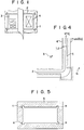
- An integrated circuit device of CMOS (Complementary Metal Oxide Semiconductor) structure, for example, a CMOS-RAM (Random Access Memory) has a p-channel MOS FET (not shown) in addition to an n-channel MOS FET (field-effected transistor) as shown in Figure 1. In Figure 1, numeral (1) denotes an n-type silicon body. Within this body (1) a p-well (2) is formed, in which in turn are formed an n+ source area or region (3) and an n+ drain area (4) respectively. In order to form a CMOS-RAM of high component desnity with an n-channel MOS FET of such a structure, it is necessary to shorten the distance between the p-well (2) and the n+ source area (3) or the distance between the p-well (2) and the n+ drain area (4). However, in such a case, punch-through phenomenon often occurs between the n+ source area (3)-p-well (2)-n body (1), and between the n+ drain area (4)-p-well (2)-n body (1) in the corners (a) of the p-well (2), causing the circuit to operate incorrectly. The cause of the punch-through phenomenon at the corners (a) of the p-well is considered to be attributable to the fact that the distance between the corners (a) of the p-well (2) and the corresponding corners of the source and drain areas (3) and (4) is smaller than the distance between the other parts of the p-well (2) and the other parts of the source and drain areas (3) and (4), that is, to the fact that the p-well (2) and the source and drain areas (3) and (4) are closest to each other at the comers (a).
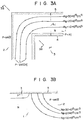
- Figure 2(a) is a plan view illustrating the impurity atom density profile in the corner of the p-well (2) shown in Figure 1. Figure 2(b) is a sectional view along the line B-B of Figure 2(a). In Figures 2(a) and (b), numeral (1) denotes an n-type silicon body; (2), a p-well; (3), an n+ source area formed in the p-well; (4), a mask used in forming the area (3); and (5), a mask used in forming the p-well (2). The material of the mask is usually a photoresist or silicon oxide.
- As may be seen Figure 2(a), Xj of the p-well, defining the area of the p-well (2) (boundary between the p-type area and the n-type area), is closest to Xj of the n+ source area (3) in the corners of the p-well (2). In particular, when the ratio of the impurity atom concentration of the p-well (2) to the impurity atom concentration of the silicon body (1) is small, that is, when the NB (impurity atom concentration) of the body (1) in Figure 2(a) is 3.Ox1015 cm-3, for example, the distance beetweenXjofthep-well(2)andXjof the n+ source (3) is, sufficient at parts other than the corners, as shown in Figure 2(a). However, the distance becomes extremely short at the corners, thereby causing punch-through phenomenon between the body (1)-the p-well (2)-the n+ area (3) at the corners.
- From Proc. of the Nat. Electr. Conference. vol. 30, 1975, pages 342-347 it is known to guard band individual elements within an LSI circuit in order to prevent surface leakage between neighbouring elements.
- A first conventional method for preventing the punch through phenomenon at the corners is to secure a sufficient distance between the maks (4) and the mask (5). This distance is shown as L1 in Figure 2(a). A second method is to decrease the impurity atom concentration (NB) of the silicon body (1). For example, NB=1.
Ox 1015 cm-3 in Figure 2(a). These methods are not, however, preferable in that they adversely affect the densification, that is the achievement of a high component density. Further, the use of a silicon body having a small impurity atom concentration limits the range of use of the silicon wafers, rendering the manufacturing cost of a semiconductor device disadvantageously high. - Figure 3(a) is a plan view illustrating the inwardly recessed corners of the p-well (2) formed in the surface of the n-type silicon body (1) and the profile of the corners of the p+ source or drain area (3) of a p-channel MOS FET formed in the surface of the body (1) in positions corresponding to the former corners. Figure 3(b) is a sectional view along the
line 3B-3B of Figure 3(a). As may be apparent from Figure 3(a), Xj of the p-well (2) and Xj of the p+ area (3) are closest in opposite corner positions. Accordingly, it is obvious that punch-through phenomenon is caused between the n-type silicon body ( 1 )―p-well (2)-p+ area (3) at these close parts, as in the case of Figure 2(a). - As may be apparent from Figure 3(a), when the impurity atom concentration (NB) of the silicon body (1) is as high as 3.0x 1015 cm-3, the distance between Xj of the p-well area (2) and X. of the p+ area (3) at the corners is sufficient. However, this apparently adversely affects the high component density of a semiconductor device and limits the impurity concentration range of the silicon wafers used. In Figure 3(a), numeral (4) denotes a mask for forming the p+ area (3); 5, a mask for forming the p-well (2); and L1, the distance between the masks (4) and (5).
- One object of the present invention is to provide a method for obtaining a higher-integrated semiconductor device.
- Another object of the present invention is to provide a semiconductor device and a method for its manufacturing in which punch-through phenomenon at the corners of the impurity area is prevented.
- A further object of the present invention is to provide a method for preventing punch-through phenomenon at the corners of the impurity area without using a silicon body having an impurity atom concentration limited to a narrow range.
- A further object of the present invention is to provide a method for controlling the shape of the corners of the impurity area.
- One aspect of the present invention provides a method for manufacturing a semiconductor device comprising forming an impurity area by supplying an impurity in a semiconductor substrate; the amount of one of the two impurities defining the corners of the impurity area is adjusted within the places where the corners are to be formed for control of the shape of the corners.
- In this method, adjustment of the amount of the impurity can be accomplished by supplying the impurity in the substrate by using a mask whose corner portions are enlarged or reduced for increasing or reducing the opening area of the mask.
- This adjustment may alternatively be accomplished by supplying an impurity of conductivity type opposite to that of the impurity area to the parts where the corners are to be formed, before or after the impurity area is formed.
- In a second aspect of the present invention, there is provided a semiconductor device having a first area of one conductivity type formed in a semiconductor substrate of the opposite conductivity type; and a second area which is formed for facing the corners of said first area and which is of the same conductivity type as said substrate; wherein the distance between corresponding corners of said first and said second areas is not smaller than that between said first and second areas excluding said corners.
- In a semiconductor device according to the second aspect, the first area is formed by introducing an impurity of conductivity type opposite to that of the substrate into the substrate by using a mask whose corner portions are enlarged or protruded for decreasing the opening area of the mask.
- In a semiconductor device according to the second aspect, the second area is alternatively formed by supplying an impurity of the same conductivity type as that of the substrate to the first area by using a mask whose corners are reduced for reducing the opening area of the mask, thereby reducing the corners of the second area. This reduction of the second area may be accompanied by supplying to the corners of the second area an impurity of the same conductivity type as that of the first area before or after forming the second area.
- In a semiconductor device according to the second aspect of the present invention, the enlargement of the first area may be accompanied by supplying to the corners of the first area an impurity of the same conductivity type as that of the first area before or after forming the first area.
- In a third aspect of the present invention, there is provided a semiconductor device having a first area which is formed within a semiconductor substrate of one conductivity, which has inwardly recessed corners, and which has a conductivity opposite to that of the substrate; and a second area which is formed in the surface of the substrate, which has the same conductivity type as that of the first area, and which has corners facing the inwardly recessed corners of the first area; wherein the distance between corresponding corners is not smaller than the distance between the first and second areas excluding the corners.
- In a semiconductor device according to the third aspect of the present invention, the first area is formed by introducing an impurity of conductivity type opposite to that of the substrate into this substrate using a mask whose inwardly recessed corners are inwardly enlarged or protruded for reducing the opening area of the mask, whereby the inwardly recessed corners of the first area are inwardly enlarged.
- In a semiconductor device according to the third aspect of the present invention, the second area is alternatively formed by supplying to the substrate an impurity of the same conductivity type as that of the first area using a mask whose corners are reduced for reducing the opening area of the mask, thereby reducing the corners of the second area.
- In a semiconductor device according to the third aspect of the present invention, the reduction of the corners of the second area may be accompanied or effected by supplying an impurity of the same conductivity type as that of the substrate to the corners of the second area before or after forming the second area.
- In a semiconductor device according to the second aspect of the present invention, the first area comprises a p-well of a complementary MOS, and the second area comprises a source or a drain of an n-channel MOS transistor.
- In a semiconductor device according to the third aspect of the present invention, the first area comprises a p-well of a complementary MOS, and the second area comprises a source or a drain of a p-channel MOS transistor.
- In a semiconductor devices according to the second or third aspect of the present invention, the distance between the first and second areas is preferably substantially constant.
- In the present invention, the supply of an impurity into the semiconductor material for forming an impurity area is performed by diffusion or ion implantation.
- This invention can be more fully understood from the following detailed description when taken in conjunction with the accompanying drawings, in which:
- Figure 1 is a plan view of a conventional semiconductor device;
- Figure 2(a) and Figure 3(a) are plan views illustrating the impurity atom density profile in the vicinity of the corners of the mask;
- Figure 2(b) and Figure 3(b) are sectional views along the
line 2B-2B of Figure 2(a) and along theline 3B-3B of Figure 3(a), respectively; - Figure 4 is a plan view illustrating the impurity atom density profile in the vicinity of the mask corners in a first embodiment of the present invention;
- Figure 5 is a plan view illustrating the overall appearance of the mask for forming a p-well in the embodiment of Figure 4;
- Figure 6(c) is a view illustrating a modification of the embodiment of Figure 4;
- Figures 6(a) and 6(b) are schematic plan views of a mask used in Figure 6(c);
- Figure 7(a) is a plan view illustrating the overall appearance of the entire mask of Figure 6(a);
- Figure 7(b) is an overall plan view of the entire maks of Figure 6(b);
- Figure 8 is a view illustrating a modification of the embodiment of Figure 4;
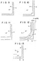
- Figures 9 to 11 are schematic plan views illustrating modifications of the mask used in the example shown in Figure 8;
- Figure 12 is a view illustrating a modification of the embodiment of Figure 4;
- Figures 13 to 16 are plan views illustrating modifications of a method for forming a p+ area (31) in Figure 12;
- Figures 17 and 18 are views illustrating modifications of the embodiment of Figure 4;
- Figure 19 is a plan view of the impurity atom density profile in the vicinity of the corners of a mask in another embodiment of the present invention;
- Figures 20 to 30 are views illustrating modifications of the example shown in Figure 19; and
- Figure 31 is a plan view of a semiconductor device according to an embodiment of the present invention.
- Figure 4 is a plan view illustrating the impurity atom density profile in the corners of the opposing first and second areas in a first embodiment of the semiconductor device according to the second aspect of the present invention.
- In Figure 4, numeral (1) denotes an n-type silicon body; (2), a p-type first area formed in the surface of the body (1), for example, a p-well of a complementary MOS: (3), an n+ second area formed in the p-well (2), for example, a source or a drain of an n-channel MOS FET; (4), a mask for forming the n+ area (3); (5), a mask for forming the p-well (2); and L21 the distance between the masks (4) and (5). In Figure 4, the same numerals designate similar parts as in Figure 2.
- As may be apparent from Figure 4, the mask (5) is so shaped that its corners are enlarged for increasing its opening area, and the enlarged part of the opening edges forms a rectangular shape. Accordingly, when the n-type impurity is supplied to the n-type body (1) using the mask (5) of this shape, that is, with its corners enlarged, the p-type impurity for forming the corners of the p-well (2) is in greater relative supply as compared to the case when the corners of the mask are not enlarged. As a result, the corners of the p-well (2) are enlarged, and the distance between Xj of the n+ area (n+Xj) and Xj of the p-well (p-well Xj) is kept substantially constant, thus preventing the local proximity of the corners of the N+Xj and the p-well Xj. Accordingly, since the position of the p-well Xj at the corners can be compensated with respect to the n+Xj, the punch-through phenomenon at the corners of the n+Xj and the p-well Xj can be prevented, even in the case wherein the distance L2 between the mask (4) and the mask (5) is smaller than in conventional cases.
- Figure 5 is an overall plan view of an example of a mask for forming the p-well (2) wherein numeral (11) denotes an enlarged part of the opening part of the mask.
- Figure 6 shows a modification of Figure 4. The mask (5) in Figure 6(a) for forming the p-well and the mask (12) with an opening (13) shown in Figure 6(b), render the same effects as derived in Figure 4. As shown in Figure 6(c), a p-type impurity is supplied to the corners of the p-well using the mask (12) before or after the supply of the p-type impurity using the mask (5). As a result of this, the corners of the p-well are compensated with impurity due to the supply of it from the opening (13) of the mask (12), so that the undesirable closeness of the corners of the p-well Xj and the n+Xj, and hence the generation of the punch-through phenomenon, is prevented. An embodiment of the method for manufacturing a semiconductor device wherein the p-well is formed in two separate steps includes the following steps:
- (1) preparing an n-type silicon wafer (NB=1.0 to 3.0x 1015 cm-3);
- (2) oxidizing the surface of this wafer;
- (3) forming the mask (5) shown in Figure 6(a) by photoetching;
- (4) supplying boron ions (amount, 1.0x 1013 cm-2) by ion implantation using this mask (5);
- (5) forming the mask (12) shown in Figure 6(a) by photoetching;
- (6) supplying boron ions (amount, 2.0x 1013 cm-2) by ion implantation through the opening (13) of the mask (12);
- (7) heating at 1200°C for slumping;
- (8) forming the mask (4) shown in Figure 6(c) by photoetching; and
- (9) forming the n+ area (3) by diffusing the n-type impurity using the mask (4).
- Figures 7(a) and 7(b) are plan views illustrating the overall appearance of the masks of Figure 6(a) and 6(b), respectively.
- Figure 8 shows an example according to the second aspect of the present invention wherein the n+ area (3) is formed by supplying an impurity of the same conductivity type as that of the n-type silicon body (1) to the p-well (2) of the first area by using a mask (4) whose corners are reduced for reducing the opening area of the mask. As may be seen from Figure 8, the mask (4) whose corners are reduced has opening edges which look as if they were formed on a right triangle. The X of the n+ area (3) formed by using the mask (4) of such a shape can maintain a sufficient distance at the corners with respect to the X of the p-well (2), thereby eliminating punch-through phenomenon. In other words, since the distance between the mask (4) for forming the n+ area and the mask (5) for forming the p-well can be shortened, densification of the integrated circuits can be facilitated.
- Figures 9 to 11 are views illustrating the modified embodiment shown in Figure 8 wherein Figure 9 shows the rounded edges of the corners of the mask (4); Figure 10 shows an example of the mask (4) whose edges look as if their corners were formed by embedding a square; and Figure 11 shows an example of the mask (4) with one side inwardly protruded so as to reduce the opening area of the mask. In all of these examples, the distance between the mask (4) for forming the n+Xj and the mask (5) for forming the p-well Xj is increased at corresponding corners. Hence, the distance between the corners of the n+Xj and the p-well Xj formed by the masks (4) and (5) is also increased. In Figures 9 to 11, the n+Xj and the p-well Xj are omitted.
- Figure 12 shows an example according to the second aspect of the present invention wherein a triangular p+ area (31) is formed by supplying an impurity of the same conductivity type as that of the first area (p-well) to the corners of the n+ area (3) before or after the second area, (n+ area 3) is formed, thereby securing a sufficient distance between the n+X and the p-well Xj at the corners. The corners of the mask (4! for forming the n+ area (3) before or after the p+ area (31) may be such that its corners are reduced as seen in the mask (4) shown in Figure 8. Alternatively, it may be such that its corners are right angled as seen in the mask (4) shown in Figure 4. In forming the n+ area (3) by using the mask (4) with right angled corners, the concentration of the p-type impurity must be higher than the concentration of the n+ area (3). Although the p+ area (31) may be formed before or after the n+ area (3), it is preferably formed simultaneously with the other p+ diffused areas constituting an integrated circuit including CMOS. The depth of the p+ area (31) is preferably shallower than the depth of the p-well but is the same as or deeper than the depth of the n+ area (3).
- Figures 13 to 16 show another embodiment of the example of Figure 12. Figure 13 shows an example wherein the shape of the p+ area (31) is rectangular and is parallel to one sides of the N+ area (3). Figure 14 is an example wherein the shape of the p+ area (31) is square instead of triangular. Figure 15 is an example wherein the shape of the p+ area (31) is such that it protrudes beyond one side of the mask (5) for forming the p-well (5). Figure 16 is an example wherein the shape of the p+ area (31) is such that it protrudes beyond the corners of the mask (5).
- In the examples shown in Figures 17 and 18, the punch-through phenomenon at the corners is prevented by inwardly reducing the corners of the mask (4) for forming the n+ area and the mask (5) for forming the p-well, thereby reducing the angles of the corners of the n+ area and the p-well.
- In Figure 17, the edges of the masks (4i and (5) are so shaped that the right angled cornr is obliquely cut away. In Figure 18, the edges of the corners of both masks (4) and (5) are curved.
- Figure 19 shows an example according to the third aspect of the present invention wherein the first area, the p-well (2), is formed by supplying a p-type impurity to the n-type silicon body (1) by using the mask (5) whose corners are protruded for reducing the opening area of the mask. As may be seen from Figure 19, the corners of the p-well (2) are inwardly recessed. That is, the distance between the p-well Xj and the p+Xj is greater at the corners than in the conventional case shown in Figure 3. Accordingly, it is possible to shorten the distance L2 between the mask (5) for forming the p-well and the mask (4) for forming the p+ area as compared to the case shown in Figure 3. In Figure 19, the same numerals denote similar parts as in Figure 3.
- Figure 20 shows another example according to the third aspect of the present invention wherein the second area whose corners are reduced is formed by supplying a p-type impurity to the n-type silicon body (1) by using the mask (4) whose corners are reduced for reducing the opening area of the mask. As may be seen from Figure 21, the edges of the corners of the mask (4) are shaped as if the right angled inner corners have been obliquely cutaway, so that the undesirable closeness between the p-well Xj and the p+Xj is prevented.
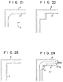
- Figures 21 to 23 show modifications of the example shown in Figure 20. Figure 21 shows an example of the mask (4) wherein the edges of the corners of the mask are rounded. Figure 22 shows an example of the
mask 4 which looks as if a square were embedded in the corner of themask 4. Figure 23 shows an example of the mask (4) wherein one side of each corner of the mask (4) is spaced apart from the mask (5) more than the other side. In these three examples, the distance between the masks (4) and (5) is increased at the corners. - Figure 24 shows an example according to the third aspect of the present invention wherein a triangular area (31) is formed by supplying an n-type impurity of the same conductivity type as that of the silicon body (1) to the corners of the p+ area (3) before or after the formation of the p+ area (3) (the second area), thereby securing a sufficient distance between the p+Xj and the p-well Xj at the comers. The particular means for forming the n+ area (31) as well as the depth of the n+ area (31) are substantially the same as described in the case of forming the p+ area (31) shown in Figure 12.
- Figures 25 through 28 show modifications of the example shown in Figure 24. Figure 25 shows an example wherein the n+ area (31) is rectangular and parallel to one side of the p+ area (3). Figure 26 shows an example wherein the shape of the n+ area is square. Figure 27 shows an example wherein the n+ area (31) is such that it protrudes beyond one side of the mask (5) for forming the p-well. Figure 28 shows an example wherein the shape of the n+ area is such that it protrudes beyond the corners of the mask (5). Figures 29 and 30 show examples wherein the angles of the corners between the p-well Xj and the p+X are made smaller, these examples corresponding to the cases of Figures 17 and 18. In Figures 29 and 30, the inwardly recessed corners of the mask (5) are outwardly enlarged for increasing the opening area of the mask, and the corners of the mask (4) are reduced for reducing the opening area of the mask. As a result, the distance between the p-well Xj and the p+Xj is, at the comers, made smaller than at the parts excluding the comers.
- Figure 31 is schematic plan view illustrating the CMOS RAM according to one embodiment of the semiconductor device of the present invention. The distance between the p-well (2) and the n+ source area (3) or the n+ drain area (4) is apparently greater at the corners (b) as compared to the case shown in Figure 1. The punch-through phenomenon will not thus occur at the corners.
- Although this description has been made with reference to CMOS FET having p-well in the above embodiments, the present invention can also be applied to CMOS FET having n-well, or integrated circuit device wherein p-well and n-well are alternately disposed.
- In summary, the present invention is advantageous in facilitating a higher integration in a semiconductor device since the distance between a plurality of impurity containing areas formed in the semiconductor substrate can be shortened. It is also advantageous in that a semiconductor substrate with a wider impurity atom concentration can be used, thereby lowering the manufacturing cost of the semiconductor device.
Claims (16)
Applications Claiming Priority (6)
| Application Number | Priority Date | Filing Date | Title |
|---|---|---|---|
| JP32254/79 | 1979-03-22 | ||
| JP3225479A JPS55125660A (en) | 1979-03-22 | 1979-03-22 | Production of semiconductor device |
| JP54145738A JPS6031109B2 (en) | 1979-11-10 | 1979-11-10 | Semiconductor device and its manufacturing method |
| JP145733/79 | 1979-11-10 | ||
| JP145738/79 | 1979-11-10 | ||
| JP14573379A JPS5669854A (en) | 1979-11-10 | 1979-11-10 | Semiconductor device and manufacture thereof |
Publications (2)
| Publication Number | Publication Date |
|---|---|
| EP0018487A1 EP0018487A1 (en) | 1980-11-12 |
| EP0018487B1 true EP0018487B1 (en) | 1983-06-29 |
Family
ID=27287636
Family Applications (1)
| Application Number | Title | Priority Date | Filing Date |
|---|---|---|---|
| EP80101439A Expired EP0018487B1 (en) | 1979-03-22 | 1980-03-19 | Semiconductor device and manufacturing method thereof |
Country Status (3)
| Country | Link |
|---|---|
| US (1) | US4533932A (en) |
| EP (1) | EP0018487B1 (en) |
| DE (1) | DE3063943D1 (en) |
Families Citing this family (3)
| Publication number | Priority date | Publication date | Assignee | Title |
|---|---|---|---|---|
| DE3063943D1 (en) * | 1979-03-22 | 1983-08-04 | Tokyo Shibaura Electric Co | Semiconductor device and manufacturing method thereof |
| US5366372A (en) * | 1993-11-29 | 1994-11-22 | Minnesota Mining And Manufacturing Company | Method and apparatus for debonding ceramic orthodontic brackets |
| KR101201903B1 (en) * | 2010-07-20 | 2012-11-16 | 매그나칩 반도체 유한회사 | Element isolation structure of semiconductor and method for forming the same |
Family Cites Families (8)
| Publication number | Priority date | Publication date | Assignee | Title |
|---|---|---|---|---|
| US3214652A (en) * | 1962-03-19 | 1965-10-26 | Motorola Inc | Transistor comprising prong-shaped emitter electrode |
| US3404295A (en) * | 1964-11-30 | 1968-10-01 | Motorola Inc | High frequency and voltage transistor with added region for punch-through protection |
| GB1140822A (en) * | 1967-01-26 | 1969-01-22 | Westinghouse Brake & Signal | Semi-conductor elements |
| US3461324A (en) * | 1967-07-03 | 1969-08-12 | Sylvania Electric Prod | Semiconductor device employing punchthrough |
| US3832732A (en) * | 1973-01-11 | 1974-08-27 | Westinghouse Electric Corp | Light-activated lateral thyristor and ac switch |
| US4066918A (en) * | 1976-09-30 | 1978-01-03 | Rca Corporation | Protection circuitry for insulated-gate field-effect transistor (IGFET) circuits |
| JPS5478092A (en) * | 1977-12-05 | 1979-06-21 | Hitachi Ltd | Lateral semiconductor device |
| DE3063943D1 (en) * | 1979-03-22 | 1983-08-04 | Tokyo Shibaura Electric Co | Semiconductor device and manufacturing method thereof |
-
1980
- 1980-03-19 DE DE8080101439T patent/DE3063943D1/en not_active Expired
- 1980-03-19 EP EP80101439A patent/EP0018487B1/en not_active Expired
-
1982
- 1982-12-20 US US06/451,412 patent/US4533932A/en not_active Expired - Lifetime
Also Published As
| Publication number | Publication date |
|---|---|
| DE3063943D1 (en) | 1983-08-04 |
| US4533932A (en) | 1985-08-06 |
| EP0018487A1 (en) | 1980-11-12 |
Similar Documents
| Publication | Publication Date | Title |
|---|---|---|
| US5427964A (en) | Insulated gate field effect transistor and method for fabricating | |
| US8067279B2 (en) | Application of different isolation schemes for logic and embedded memory | |
| US5439835A (en) | Process for DRAM incorporating a high-energy, oblique P-type implant for both field isolation and punchthrough | |
| US6100143A (en) | Method of making a depleted poly-silicon edged MOSFET structure | |
| US5793088A (en) | Structure for controlling threshold voltage of MOSFET | |
| US4912053A (en) | Ion implanted JFET with self-aligned source and drain | |
| US6258645B1 (en) | Halo structure for CMOS transistors and method of manufacturing the same | |
| EP0470716A2 (en) | Process for forming MOS devices in VLSI structures | |
| US5441906A (en) | Insulated gate field effect transistor having a partial channel and method for fabricating | |
| US5557129A (en) | Semiconductor MOSFET device having a shallow nitrogen implanted channel region | |
| US5212542A (en) | Semiconductor device having at least two field effect transistors and method of manufacturing the same | |
| US5623154A (en) | Semiconductor device having triple diffusion | |
| US4533932A (en) | Semiconductor device with enlarged corners to provide enhanced punch through protection | |
| KR0138234B1 (en) | Structure of high voltage mos transistor | |
| KR100205194B1 (en) | Semiconductor device and manufacturing method | |
| KR100513445B1 (en) | Method for manufacturing semiconductor device | |
| US5110750A (en) | Semiconductor device and method of making the same | |
| KR100263909B1 (en) | Method for forming multiple well of semiconductor integrated circuit | |
| KR20010067470A (en) | Semiconductor device and method of fabricating the same | |
| JP3430102B2 (en) | Method for manufacturing semiconductor device | |
| US6507058B1 (en) | Low threshold compact MOS device with channel region formed by outdiffusion of two regions and method of making same | |
| JPH05283629A (en) | Semiconductor device and its manufacture | |
| CN1173739A (en) | Semiconductor device and its manufacturing method | |
| US6881634B2 (en) | Buried-channel transistor with reduced leakage current | |
| US6432759B1 (en) | Method of forming source and drain regions for CMOS devices |
Legal Events
| Date | Code | Title | Description |
|---|---|---|---|
| PUAI | Public reference made under article 153(3) epc to a published international application that has entered the european phase |
Free format text: ORIGINAL CODE: 0009012 |
|
| 17P | Request for examination filed | ||
| AK | Designated contracting states |
Designated state(s): DE FR GB |
|
| GRAA | (expected) grant |
Free format text: ORIGINAL CODE: 0009210 |
|
| AK | Designated contracting states |
Designated state(s): DE FR GB |
|
| REF | Corresponds to: |
Ref document number: 3063943 Country of ref document: DE Date of ref document: 19830804 |
|
| EL | Fr: translation of claims filed | ||
| PLBE | No opposition filed within time limit |
Free format text: ORIGINAL CODE: 0009261 |
|
| STAA | Information on the status of an ep patent application or granted ep patent |
Free format text: STATUS: NO OPPOSITION FILED WITHIN TIME LIMIT |
|
| 26N | No opposition filed | ||
| REG | Reference to a national code |
Ref country code: FR Ref legal event code: CD |
|
| REG | Reference to a national code |
Ref country code: GB Ref legal event code: 746 |
|
| PGFP | Annual fee paid to national office [announced via postgrant information from national office to epo] |
Ref country code: DE Payment date: 19970401 Year of fee payment: 18 |
|
| PGFP | Annual fee paid to national office [announced via postgrant information from national office to epo] |
Ref country code: GB Payment date: 19980310 Year of fee payment: 19 Ref country code: FR Payment date: 19980310 Year of fee payment: 19 |
|
| PG25 | Lapsed in a contracting state [announced via postgrant information from national office to epo] |
Ref country code: DE Free format text: LAPSE BECAUSE OF NON-PAYMENT OF DUE FEES Effective date: 19981201 |
|
| PG25 | Lapsed in a contracting state [announced via postgrant information from national office to epo] |
Ref country code: GB Free format text: LAPSE BECAUSE OF NON-PAYMENT OF DUE FEES Effective date: 19990319 |
|
| GBPC | Gb: european patent ceased through non-payment of renewal fee |
Effective date: 19990319 |
|
| PG25 | Lapsed in a contracting state [announced via postgrant information from national office to epo] |
Ref country code: FR Free format text: LAPSE BECAUSE OF NON-PAYMENT OF DUE FEES Effective date: 19991130 |
|
| REG | Reference to a national code |
Ref country code: FR Ref legal event code: ST |