EP0017596B1 - Low noise photoreceiver - Google Patents
Low noise photoreceiver Download PDFInfo
- Publication number
- EP0017596B1 EP0017596B1 EP80400472A EP80400472A EP0017596B1 EP 0017596 B1 EP0017596 B1 EP 0017596B1 EP 80400472 A EP80400472 A EP 80400472A EP 80400472 A EP80400472 A EP 80400472A EP 0017596 B1 EP0017596 B1 EP 0017596B1
- Authority
- EP
- European Patent Office
- Prior art keywords
- level
- output
- signal
- transducer
- main amplifier
- Prior art date
- Legal status (The legal status is an assumption and is not a legal conclusion. Google has not performed a legal analysis and makes no representation as to the accuracy of the status listed.)
- Expired
Links
- 238000005286 illumination Methods 0.000 claims abstract 2
- 108091008695 photoreceptors Proteins 0.000 description 11
- 230000010287 polarization Effects 0.000 description 11
- 241001644893 Entandrophragma utile Species 0.000 description 7
- 238000010586 diagram Methods 0.000 description 6
- 230000000694 effects Effects 0.000 description 3
- 235000021183 entrée Nutrition 0.000 description 3
- 230000007423 decrease Effects 0.000 description 2
- 241001080024 Telles Species 0.000 description 1
- 230000003321 amplification Effects 0.000 description 1
- 238000004458 analytical method Methods 0.000 description 1
- 230000005540 biological transmission Effects 0.000 description 1
- 238000001914 filtration Methods 0.000 description 1
- 230000004907 flux Effects 0.000 description 1
- 238000003199 nucleic acid amplification method Methods 0.000 description 1
- 230000003287 optical effect Effects 0.000 description 1
- 239000004065 semiconductor Substances 0.000 description 1
- 238000000926 separation method Methods 0.000 description 1
Images
Classifications
-
- H—ELECTRICITY
- H03—ELECTRONIC CIRCUITRY
- H03G—CONTROL OF AMPLIFICATION
- H03G3/00—Gain control in amplifiers or frequency changers without distortion of the input signal
- H03G3/20—Automatic control
- H03G3/30—Automatic control in amplifiers having semiconductor devices
- H03G3/3084—Automatic control in amplifiers having semiconductor devices in receivers or transmitters for electromagnetic waves other than radiowaves, e.g. lightwaves
-
- G—PHYSICS
- G01—MEASURING; TESTING
- G01S—RADIO DIRECTION-FINDING; RADIO NAVIGATION; DETERMINING DISTANCE OR VELOCITY BY USE OF RADIO WAVES; LOCATING OR PRESENCE-DETECTING BY USE OF THE REFLECTION OR RERADIATION OF RADIO WAVES; ANALOGOUS ARRANGEMENTS USING OTHER WAVES
- G01S7/00—Details of systems according to groups G01S13/00, G01S15/00, G01S17/00
- G01S7/48—Details of systems according to groups G01S13/00, G01S15/00, G01S17/00 of systems according to group G01S17/00
- G01S7/491—Details of non-pulse systems
- G01S7/493—Extracting wanted echo signals
-
- H—ELECTRICITY
- H01—ELECTRIC ELEMENTS
- H01J—ELECTRIC DISCHARGE TUBES OR DISCHARGE LAMPS
- H01J43/00—Secondary-emission tubes; Electron-multiplier tubes
- H01J43/04—Electron multipliers
- H01J43/30—Circuit arrangements not adapted to a particular application of the tube and not otherwise provided for
-
- H—ELECTRICITY
- H01—ELECTRIC ELEMENTS
- H01L—SEMICONDUCTOR DEVICES NOT COVERED BY CLASS H10
- H01L31/00—Semiconductor devices sensitive to infrared radiation, light, electromagnetic radiation of shorter wavelength or corpuscular radiation and specially adapted either for the conversion of the energy of such radiation into electrical energy or for the control of electrical energy by such radiation; Processes or apparatus specially adapted for the manufacture or treatment thereof or of parts thereof; Details thereof
- H01L31/02—Details
- H01L31/02016—Circuit arrangements of general character for the devices
- H01L31/02019—Circuit arrangements of general character for the devices for devices characterised by at least one potential jump barrier or surface barrier
- H01L31/02027—Circuit arrangements of general character for the devices for devices characterised by at least one potential jump barrier or surface barrier for devices working in avalanche mode
-
- H—ELECTRICITY
- H04—ELECTRIC COMMUNICATION TECHNIQUE
- H04B—TRANSMISSION
- H04B10/00—Transmission systems employing electromagnetic waves other than radio-waves, e.g. infrared, visible or ultraviolet light, or employing corpuscular radiation, e.g. quantum communication
- H04B10/60—Receivers
Definitions
- the present invention relates to photoreceptor devices, and applies in particular to telecommunications and electro-optical telemetry.
- Photoreceptor devices are already known comprising a photoelectric transducer with polarization variable multiplying factor, such as an avalanche photodiode or a photomultiplier tube. To this transducer are added a controlled polarization circuit, a main amplifier mounted between the output of the photomultiplier and the output terminal of the photoreceptor device, and a bias control chain mounted between the output of the main amplifier and the input. of the polarization circuit.
- electro-optical rangefinders currently operate at a very long distance, and it is the signal-to-noise ratio of the photoreceptor transducer that defines the maximum suitable operating distance.
- the main object of the present invention is to provide a photoreceptor device having a very suitable signal-to-noise ratio.
- the output terminal finally gives the useful signal, a noise multiplied by the transducer, due to the ambient lighting as well as to the specific characteristics of the transducer, and a noise not multiplied by the transducer, due only to specific characteristics of the transducer and the main amplifier.
- the auxiliary signal By passing the auxiliary signal through the main amplifier, one avoids the temperature drifts of the electronic circuits, since this auxiliary signal crosses the same amplifier stages as the useful signal and the noises.
- the multiplication of the useful signal level by the transducer being proportional to M 2
- the multiplication of the noise level by the transducer being proportional to M d , where is a quantity linked to the transducer, and which varies between 2.3 and 3 as a function of the multiplier factor M, K is less than
- the servo chain prefferably includes a broadband amplifier inserted between the output of the main amplifier and the inputs of the two detector circuits.
- the auxiliary signal is an alternating sinusoidal signal.
- Said predetermined polarization imposed by the polarization circuit when the level N s of the useful signal is much higher than the levels N b and N x of the noises is advantageously chosen to define a multiplying factor equal to a few units approximately.
- the photoelectric transducer used according to the present invention is preferably an avalanche photodiode, but it is also possible to use a photomultiplier tube.
- the Applicant has also observed that the use of avalanche gain in an avalanche photodiode makes it possible to increase the output signal of the photodiode, and thereby reduce the effect of the noise of the amplifier which follows it.
- the practical problem is that beyond a certain threshold, which varies with temperature, the increase in the multiplying factor of the avalanche photodiode is accompanied by a very rapid increase in noise.
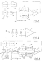
- FIG. 1 illustrates the block diagram of a photodetector device according to the invention.
- an avalanche photodiode 10 receives a light flux 0 consisting for example of an infrared beam modulated at a frequency F of the order of 10 MHz.
- the output of the photodiode 10, including an electrical signal of frequency F, is applied to a main amplifier; and the output thereof gives on the output terminal 12, in addition to the noises, a useful signal which will then be processed by the reception circuits of a range finder.
- the avalanche photodiode 10 receives a polarization voltage defined by the polarization control circuit 15, from a high voltage supply circuit 16 (the polarization voltages commonly reach one hundred volts).
- the useful signal current i s depends on the useful photocurrent I Ph , in the photodiode, on the modulation index m of the received light beam, as well as on the multiplier factor M of the avalanche photodiode; the mean value of the useful signal level is written:
- the average value of the amplified noise level can be written:
- the unamplified noise current i x depends on the series resistance of the photodiode, its surface leakage current, and the noise current of the amplifier stage, reduced to its input. These parameters, which can be known in advance, are noted l x .
- the average value of the non-amplified noise level is written:
- N x is known in advance.
- N b + Nx K where K is less than [d / (d - 2)] N , which is known in advance.
- K is less than [d / (d - 2)] N , which is known in advance.
- values of K very close to [d / (d - 2)] N x may be suitable, but it is generally desirable to take a value of K which is not too close to
- a detector circuit 13 ( Figure 1) rectifies the output of the main amplifier 11, thus providing a level: signal which is applied to a first input of a comparator 14.
- a reference circuit 20 produces an auxiliary reference level, predetermined, equal to K, applied to the second input of comparator 14.
- the levels of useful signal N s and of multiplied noise N b participate together in the control of the multiplier factor M, which provides automatic gain control, an advantageous property in particular in rangefinders.
- the automatic gain control is essentially carried out according to the useful signal.
- the polarization circuit fixes a predetermined polarization of the photodiode, corresponding to a small multiplying factor of the order of a few units (5 for example).
- the gain M is constant, and the servo no longer acts.
- the signal level can be adjusted, if necessary, by acting on the optical transmission of the system (diaphragm; gray filter) or on the gain of the electronics downstream of 12.
- the reference signal is applied to the input of the main amplifier 11, with the output signal of the photodiode 10. It retains the level 2 ⁇ N x , taking into account the amplification factors concerned; but it consists of a signal located in a frequency band outside that of the useful signal. Preferably, it is a pure sinusoidal signal whose frequency F r is of the order of 7 to 8 MHz.
- the output of the main amplifier 11 is applied to a wideband auxiliary amplifier 17, followed by the aforementioned detector circuit 13, which now includes a notch filter eliminating the frequency band from the reference signal, then a level detector 131 , the output of which arrives at the first input of comparator 14.
- a second detector assembly also connected to the output of the broadband amplifier 17, comprises a bandpass filter 230, selecting the frequency band of the reference signal, then a level detector 231, the output of which is connected to the second input of comparator 14.
- the device of the invention appreciably improves the performance of a photoreceptor device with an avalanche photodiode. This applies in particular to electro-optical rangefinders operating at long distance, regardless of the ambient lighting.
Abstract
Description
La présente invention concerne les dispositifs photorécepteurs, et s'applique en particulier aux télécommunications et en télémétrie électro-optique.The present invention relates to photoreceptor devices, and applies in particular to telecommunications and electro-optical telemetry.
On connaît déjà des dispositifs photorécepteurs comportant un transducteur photoélectrique à facteur multiplicateur variable par polarisation, tel qu'une photodiode à avalanche ou un tube photomultiplicateur. A ce transducteur sont ajoutés un circuit commandé de polarisation, un amplificateur principal monté entre la sortie du photomultiplicateur et la borne de sortie du dispositif photorécepteur, et une chaîne d'asservissement de polarisation montée entre la sortie de l'amplificateur principal et l'entrée de commande du circuit de polarisation.Photoreceptor devices are already known comprising a photoelectric transducer with polarization variable multiplying factor, such as an avalanche photodiode or a photomultiplier tube. To this transducer are added a controlled polarization circuit, a main amplifier mounted between the output of the photomultiplier and the output terminal of the photoreceptor device, and a bias control chain mounted between the output of the main amplifier and the input. of the polarization circuit.
Un tel dispositif est par exemple décrit dans le document « The Review of Scientific Instruments •, volume 41, n° 8, août 1978.Such a device is for example described in the document "The Review of Scientific Instruments •, volume 41, n ° 8, August 1978.
Différentes structures ont été proposées pour la chaîne d'asservissement. Le plus souvent en vue de compenser l'effet des variations de température sur le facteur multiplicateur du transducteur. De telles chaînes d'asservissement visent donc à stabiliser le point de polarisation du transducteur qui est en général une photodiode à avalanche.Different structures have been proposed for the servo chain. Most often in order to compensate for the effect of temperature variations on the multiplier factor of the transducer. Such control chains therefore aim to stabilize the polarization point of the transducer which is generally an avalanche photodiode.
De nombreuses applications, et en particulier la télémétrie électro-optique, nécessitent que l'on obtienne un excellent rapport signal sur bruit. En effet, les télémètres électro-optiques opèrent à l'heure actuelle à très grande distance, et c'est le rapport signal sur bruit du transducteur photorécepteur qui définit la distance maximale de fonctionnement convenable.Many applications, and in particular electro-optical telemetry, require an excellent signal-to-noise ratio. In fact, electro-optical rangefinders currently operate at a very long distance, and it is the signal-to-noise ratio of the photoreceptor transducer that defines the maximum suitable operating distance.
La présente invention a essentiellement pour but de fournir un dispositif photorécepteur présentant un rapport signal sur bruit très adapté.The main object of the present invention is to provide a photoreceptor device having a very suitable signal-to-noise ratio.
La demanderesse a observé que, dans un dispositif récepteur du type précité, la borne de sortie donne finalement le signal utile, un bruit multiplié par le transducteur, dû à l'éclairement ambiant ainsi qu'à des caractéristiques propres du transducteur, et un bruit non multiplié par le transducteur, dû seulement à des caractéristiques propres du transducteur et de l'amplificateur principal.The Applicant has observed that, in a receiver device of the aforementioned type, the output terminal finally gives the useful signal, a noise multiplied by the transducer, due to the ambient lighting as well as to the specific characteristics of the transducer, and a noise not multiplied by the transducer, due only to specific characteristics of the transducer and the main amplifier.
Cette analyse est également développée dans le document IEEE Transactions ou Electron Devices Vol. ED 14, N° 5, mai 1967.This analysis is also developed in the document IEEE Transactions or Electron Devices Vol. ED 14, No. 5, May 1967.
Le dispositif photorécepteur pour signal utile à bande étroite conforme à l'invention est du type comprenant un transducteur photomultiplicateur associé à un circuit de polarisation commandée qui en règle le facteur multiplicateur, un amplificateur principal monté entre la sortie du photomultiplicateur et la borne de sortie du dispositif photorécepteur, ainsi qu'une chaîne d'asservissement de polarisation montée entre la sortie de l'amplificateur principal et l'entrée de commande du circuit de polarisation, dispositif dans lequel,
- - étant observé que la borne de sortie donne finalement le signal utile, de niveau NS, un bruit multiplié par le transducteur de niveau Nb, dû à l'éclairement ambiant ainsi qu'à des caractéristiques propres du transducteur, et un bruit non multiplié par le transducteur, de niveau N,, dû seulement à des caractéristiques propres du transducteur et de l'amplificateur principal, ces niveaux de bruit étant rapportés à la même largeur de bande de référence,
- - la chaîne d'asservissement comporte :
- un circuit détecteur de niveau relié à la sortie de l'amplificateur pour en détecter le niveau de sortie d'ensemble N, + Nb + Nx,
- un générateur de signal auxiliaire de niveau prédéterminé lié à un niveau de référence K, et un
comparateur dont les deux entrées reçoivent respectivement la sortie du circuit détecteur et un signal tiré de la sortie du générateur de signal auxiliaire, tandis que sa sortie commande le circuit de polarisation, pour que celui-ci fasse respecter la relation :
- - le dispositif étant caractérisé selon l'invention par le fait que
- - le générateur de signal auxiliaire produit un signal dont la bande de fréquences est disjointe de celle du signal utile du transducteur,
- - ce signal est appliqué à l'entrée de l'amplificateur principal avec la sortie du phototransducteur,
- - le circuit détecteur comporte un filtre coupe-bande relié à la sortie de l'amplificateur principal, éliminant le signal auxiliaire et suivi d'un étage détecteur de niveau, ainsi qu'un filtre passe-bande relié à la sortie de l'amplificateur principal, sélectionnant le signal auxiliaire et suivi d'un second étage détecteur de niveau, et
- - le comparateur reçoit en entrée les sorties respectives des deux étages détecteurs de niveau, de telle sorte que :
- - lorsque le niveau Ns du signal utile est très inférieur aux niveaux de bruit Nb et Nx, la condition d'asservissement est Nb + Nx = K,
- - lorsque le niveau Ns du signal utile est du même ordre que celui des bruits, étant observé que le bruit amplifié est alors négligeable, l'asservissement fonctionne en contrôle automatique de gain afin de maintenir sensiblement constant le signal de sortie du dispositif photorécepteur,
- - tandis que lorsque le niveau N, du signal utile est largement supérieur aux niveaux Nb et Nx des bruits, le circuit de polarisation produit une polarisation prédéterminée correspondant à un facteur multiplicateur minimal.
- - it being observed that the output terminal finally gives the useful signal, of level N S , a noise multiplied by the transducer of level N b , due to the ambient lighting as well as to the specific characteristics of the transducer, and a noise not multiplied by the transducer, level N ,, due only to the specific characteristics of the transducer and the main amplifier, these noise levels being related to the same reference bandwidth,
- - the control chain includes:
- a level detector circuit connected to the output of the amplifier to detect the overall output level N, + N b + N x ,
- an auxiliary signal generator of predetermined level linked to a reference level K, and a
comparator, the two inputs of which respectively receive the output of the detector circuit and a signal drawn from the output of the auxiliary signal generator, while its output controls the bias circuit, so that the latter makes respect for the relationship:
- - the device being characterized according to the invention in that
- the auxiliary signal generator produces a signal whose frequency band is disjoint from that of the useful signal of the transducer,
- - this signal is applied to the input of the main amplifier with the output of the phototransducer,
- - the detector circuit includes a notch filter connected to the output of the main amplifier, eliminating the auxiliary signal and followed by a level detector stage, as well as a bandpass filter connected to the output of the amplifier main, selecting the auxiliary signal and followed by a second stage level detector, and
- - the comparator receives as input the respective outputs of the two level detector stages, so that:
- - when the level N s of the useful signal is much lower than the noise levels N b and N x , the control condition is N b + N x = K,
- - when the level N s of the useful signal is of the same order as that of the noises, it being observed that the amplified noise is then negligible, the control operates in automatic gain control in order to keep the output signal of the photoreceptor device substantially constant,
- - while when the level N, of the useful signal is much higher than the levels N b and N x of the noises, the bias circuit produces a predetermined bias corresponding to a minimum multiplying factor.
En faisant transiter le signal auxiliaire par l'amplificateur principal, on s'affranchit des dérives en températures des circuits électroniques, puisque ce signal auxiliaire traverse les mêmes étages amplificateurs que le signal utile et les bruits. Très avantageusement, la multiplication du niveau de signal utile par le transducteur étant proportionnelle à M2, et la multiplication du niveau de bruit par le transducteur étant proportionnelle à Md, où est une grandeur liée au transducteur, et qui évolue entre 2,3 et 3 en fonction du facteur multiplicateur M, K est inférieur à![]()
![]()
Il s'est également avéré avantageux que la chaîne d'asservissement comporte un amplificateur à large bande inséré entre la sortie de l'amplificateur principal et les entrées des deux circuits détecteurs.It has also proved advantageous for the servo chain to include a broadband amplifier inserted between the output of the main amplifier and the inputs of the two detector circuits.
Dans un mode de réalisation particulier le signal auxiliaire est un signal alternatif sinusoïdal.In a particular embodiment, the auxiliary signal is an alternating sinusoidal signal.
Ladite polarisation prédéterminée imposée par le circuit de polarisation lorsque le niveau Ns du signal utile est largement supérieur aux niveaux Nb et Nx des bruits est avantageusement choisie pour définir un facteur multiplicateur égal à quelques unités environ.Said predetermined polarization imposed by the polarization circuit when the level N s of the useful signal is much higher than the levels N b and N x of the noises is advantageously chosen to define a multiplying factor equal to a few units approximately.
Le transducteur photoélectrique utilisé selon la présente invention est de préférence une photodiode à avalanche, mais on peut également utiliser un tube photomultiplicateur.The photoelectric transducer used according to the present invention is preferably an avalanche photodiode, but it is also possible to use a photomultiplier tube.
D'autres caractéristiques et avantages de l'invention apparaîtront à la lecture de la description détaillée qui va suivre, faite en référence aux dessins annexés, sur lesquels :
- la Figure 1 est le schéma de principe d'un dispositif photorécepteur selon la présente invention ;
- la Figure 2 est un schéma électrique équivalent permettant de définir le niveau du signal utile du transducteur, le niveau du bruit amplifié par le transducteur, et le niveau du bruit non amplifié par celui-ci ;
- la Figure 3 est le schéma électrique de principe d'un mode de réalisation préférentiel de l'invention ; et
- les Figures 4 et 5 sont différents diagrammes illustrant les relations entre des grandeurs entrant en ligne de compte selon l'invention.
- Figure 1 is the block diagram of a photoreceptor device according to the present invention;
- FIG. 2 is an equivalent electrical diagram making it possible to define the level of the useful signal from the transducer, the level of noise amplified by the transducer, and the level of noise not amplified by the latter;
- Figure 3 is the block diagram of a preferred embodiment of the invention; and
- Figures 4 and 5 are different diagrams illustrating the relationships between quantities taken into account according to the invention.
La description détaillée qui va suivre vise une application de télémétrie électro-optique.The detailed description which follows relates to an electro-optical telemetry application.
On sait que ces télémètres utilisent un rayon lumineux modulé en amplitude à une fréquence assez élevée, voisine de 10 MHz en général. Un photo-récepteur permet de retrouver le signal de modulation, qui est immédiatement appliqué à un étage amplificateur à faible bruit. La demanderesse a observé que la puissance équivalente au bruit de l'ensemble comprenant une photodiode semi-conductrice classique et un étage amplificateur à faible bruit, ramenée à l'entrée de la photodiode, était largement supérieure à la puissance de bruit de la photodiode classique elle-même. Il apparaît donc que la limitation sur le plan du bruit d'un dispositif photorécepteur à photodiode classique est due au premier étage amplificateur qui suit la diode.We know that these rangefinders use a light beam amplitude modulated at a fairly high frequency, close to 10 MHz in general. A photo-receiver makes it possible to find the modulation signal, which is immediately applied to a low noise amplifier stage. The Applicant has observed that the power equivalent to the noise of the assembly comprising a conventional semiconductor photodiode and a low noise amplifier stage, brought back to the input of the photodiode, was much greater than the noise power of the conventional photodiode herself. It therefore appears that the noise limitation of a conventional photodiode photoreceptor device is due to the first amplifier stage which follows the diode.
La demanderesse a observé également que l'emploi du gain d'avalanche dans une photodiode à avalanche permet d'augmenter le signal de sortie de la photodiode, et par là de réduire l'effet du bruit de l'amplificateur qui la suit. Le problème pratique est qu'au delà d'un certain seuil, variable avec la température, l'augmentation du facteur multiplicateur de la photodiode à avalanche s'accompagne d'une augmentation très rapide du bruit.The Applicant has also observed that the use of avalanche gain in an avalanche photodiode makes it possible to increase the output signal of the photodiode, and thereby reduce the effect of the noise of the amplifier which follows it. The practical problem is that beyond a certain threshold, which varies with temperature, the increase in the multiplying factor of the avalanche photodiode is accompanied by a very rapid increase in noise.
La Figure 1 illustre le schéma de principe d'un dispositif photodétecteur selon l'invention. Classiquement, une photodiode à avalanche 10 reçoit un flux lumineux 0 constitué par exemple d'un faisceau infrarouge modulé à une fréquence F de l'ordre de 10 MHz. La sortie de la photodiode 10, dont un signal électrique de fréquence F, est appliquée à un amplificateur principal ; et la sortie de celui-ci donne sur la borne de sortie 12, en plus des bruits, un signal utile qui sera traité ensuite par les circuits de réception d'un télémètre.Figure 1 illustrates the block diagram of a photodetector device according to the invention. Conventionally, an
La photodiode à avalanche 10 reçoit une tension de polarisation définie par le circuit de commande de polarisation 15, à partir d'un circuit d'alimentation haute tension 16 (les tensions de polarisation atteignent couramment la centaine de volts).The
La demanderesse a fait différentes observations, à partir du schéma équivalent de la Figure 2 qui est une représentation en sources de courant de l'entrée de l'amplificateur principal 11 :
- - is désigne le courant associé au signal utile ;
- - ib désigne le courant associé au bruit multiplié par la photodiode, car dépendant de l'avalanche, et
- - ix désigne le courant associé au bruit non multiplié par l'avalanche.
- - i s denotes the current associated with the useful signal;
- - i b denotes the current associated with the noise multiplied by the photodiode, since it depends on the avalanche, and
- - i x denotes the current associated with the noise not multiplied by the avalanche.
Le courant de signal utile is dépend du photocourant utile IPh, dans la photodiode, de l'indice de modulation m du faisceau lumineux reçu, ainsi que du facteur multiplicateur M de la photodiode à avalanche ; la valeur moyenne du niveau de signal utile s'écrit :![]()
![]()
Le courant de bruit amplifié ib dépend de la somme lPho + lo du photocourant total Ipho pour M = 1 (y compris l'éclairement ambiant), et du courant de fuite en volume lo de la photodiode, de la largeur de bande Δf, de la charge q d'un électron, et d'un coefficient d, compris généralement entre 2,3 et 3, et caractéristique de la photodiode.The amplified noise current i b depends on the sum l Pho + l o of the total photocurrent Ip ho for M = 1 (including the ambient lighting), and of the leakage current in volume l o of the photodiode, of the width band Δf, the charge q of an electron, and a coefficient d, generally between 2.3 and 3, and characteristic of the photodiode.
La valeur moyenne du niveau de bruit amplifié peut s'écrire :![]()
![]()
Enfin, le courant de bruit non amplifié ix dépend de la résistance série de la photodiode, de son courant de fuite de surface, et du courant de bruit de l'étage amplificateur, ramené à son entrée. Ces paramètres, qui peuvent être connus à l'avance, sont notés lx. La valeur moyenne du niveau de bruit non amplifié s'écrit :![]()
![]()
On notera que Nx est connu à l'avance.Note that N x is known in advance.
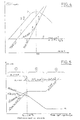
En écrivant le rapport signal sur bruit y = Ns/(Nb + Nx), on observe que celui-ci est maximal (courbe D : Figure 4) pour![]()
![]()
La demanderesse a finalement remarqué qu'à cette relation correspond la condition suivante sur le bruit total :![]()
![]()
L'expérience a cependant montré que, pour éviter des instabilités, il est important de prendre Nb + Nx = K où K est inférieur à [d/(d - 2)] N,, qui est connu à l'avance. Pour certaines applications, des valeurs de K très voisines de [d/(d - 2)] Nx peuvent convenir, mais il est généralement souhaitable de prendre une valeur de K qui ne soit pas trop proche de![]()
![]()
On reviendra maintenant à la réalisation de la Figure 1.We will now return to the embodiment of Figure 1.
Un circuit détecteur 13 (Figure 1) redresse la sortie de l'amplificateur principal 11, fournissant donc un niveau :![]()
![]()
Un circuit de référence 20 produit un niveau auxiliaire de référence, prédéterminé, égal à K, appliqué à la seconde entrée du comparateur 14.A
Celui-ci agit donc sur le circuit de polarisation 15 en tant qu'asservissement de constante de temps convenable pour faire respecter la relation :![]()
![]()
On voit immédiatement que cette condition n'est pas identique à Nb + Nx = K. Elle se confond cependant avec elle aux faibles valeurs du signal utile (zone 1 ; Figure 5), là où un très bon rapport signal sur bruit est important. Et elle est très simple à réaliser, ne nécessitant aucune séparation du signal utile et des différents bruits.We can immediately see that this condition is not identical to N b + N x = K. It however merges with it at the low values of the useful signal (
Aux valeurs intermédiaires du signal utile (frontières zones 1 et 2 ; Figure 5), pour lesquelles le bruit amplifié n'est pas encore négligeable devant le signal utile, les niveaux de signal utile Ns et de bruit multiplié Nb participent ensemble à l'asservissement du facteur multiplicateur M, ce qui fournit une commande automatique de gain, propriété intéressante en particulier dans les télémètres. Dans la zone 2, la commande automatique de gain se fait essentiellement d'après le signal utile.At the intermediate values of the useful signal (
Enfin, en présence d'un fort signal utile (zone 3 ; Figure 5), le circuit de polarisation fixe une polarisation prédéterminée de la photodiode, correspondant à un faible facteur multiplicateur de l'ordre de quelques unités (5 par exemple).Finally, in the presence of a strong useful signal (
En ce qui concerne le rapport K/Nx = [d/(d - 2)] celui-ci doit être inférieur à 7,67 pour des photodiodes à avalanche où d = 2,3 dans la zone des gains intermédiaires ; cette limite descend progressivement aux valeurs extrêmes du gain ou pour des photodiodes dont d minimum est plus grand que 2,3.Regarding the ratio K / N x = [d / (d - 2)] this must be less than 7.67 for avalanche photodiodes where d = 2.3 in the zone of intermediate gains; this limit gradually descends to the extreme gain values or for photodiodes whose minimum d is greater than 2.3.
La demanderesse a considéré que la valeur K = 2 · Nx est satisfaisante pour l'application aux télémètres, et convient pour la quasi-totalité des photodiodes à avalanche actuellement disponibles.The Applicant has considered that the value K = 2 · N x is satisfactory for application to range finders, and is suitable for almost all of the avalanche photodiodes currently available.
On remarquera qu'avec K = 2 · Nx, la condition d'asservissement s'écrit Ns + Nb = Nx. En présence d'un fort signal utile, le terme Nb devient négligeable, et l'on obtient Ns = Nx. Corrélativement le rapport signal sur bruit est égal à l'unité, mais en considérant toute la largeur de bande Δf. Comme le signal utile occupe une petite largeur de bande (obtenue par filtrage dans des circuits récepteurs du télémètre, non représentés), il suffit de choisir Δf suffisamment grand pour avoir le rapport signal sur bruit désiré.Note that with K = 2 · N x , the servo condition is written N s + N b = N x . In the presence of a strong useful signal, the term N b becomes negligible, and we obtain N s = N x . Correlatively the signal-to-noise ratio is equal to unity, but considering the entire bandwidth Δf. Since the useful signal occupies a small bandwidth (obtained by filtering in rangefinder receiver circuits, not shown), it suffices to choose Δf large enough to have the desired signal-to-noise ratio.
La Figure 5 résume le fonctionnement de l'asservissement et illustre schématiquement les variations en échelle logarithmique de M, (Nb + Nx) et Ns en fonction du niveau de photocourant utile (lPh)2 pour M = 1, également en échelle logarithmique :
- ― pour (lPh)2 < So, l'asservissement maintient Nb = Nx ; le facteur M décroît avec le niveau de signal (lPh)2 tandis que le rapport signal sur bruit y croît (zone 1) ; on voit l'influence de l'éclairement ambiant l0.
- ― à partir de (lPh)2 = So (zone 2), le rapport signal bruit y est maintenu constant ; de son côté, le facteur M continue à décroître, et avec lui le bruit amplifié par la photodiode Nb.
- - for (l Ph ) 2 <S o , the control maintains N b = N x ; the factor M decreases with the signal level (l Ph ) 2 while the signal to noise ratio increases there (zone 1); we can see the influence of the ambient lighting l 0 .
- - from (l Ph ) 2 = S o (zone 2), the signal-to-noise ratio is kept constant there; for its part, the factor M continues to decrease, and with it the noise amplified by the photodiode N b .
Dans la zone 3, le gain M est constant, et l'asservissement n'agit plus. L'ajustement du niveau de signal peut se faire, si nécessaire, en agissant sur la transmission optique du système (diaphragme ; filtre gris) ou sur le gain de l'électronique en aval de 12.In
On décrira maintenant, en référence à la Figure 3, le mode de réalisation actuellement préféré de l'invention.We will now describe, with reference to Figure 3, the currently preferred embodiment of the invention.
Le signal de référence est appliqué à l'entrée de l'amplificateur principal 11, avec le signal de sortie de la photodiode 10. II conserve le niveau 2 · Nx, en tenant compte des facteurs d'amplification concernés ; mais il est constitué d'un signal situé dans une bande de fréquences extérieur à celle du signal utile. De préférence, c'est un signal sinusoïdal pur dont la fréquence Fr est de l'ordre de 7 à 8 MHz.The reference signal is applied to the input of the
La sortie de l'amplificateur principal 11 est appliquée à un amplificateur auxiliaire à large bande 17, suivi du circuit détecteur 13 précité, lequel comporte maintenant un filtre coupe-bande éliminant la bande de fréquences du signal de référence, puis un détecteur de niveau 131, dont la sortie arrive à la première entrée du comparateur 14.The output of the
Un second ensemble détecteur, également connecté à la sortie de l'amplificateur à large bande 17, comprend un filtre passe bande 230, sélectionnant la bande de fréquences du signal de référence, puis un détecteur de niveau 231, dont la sortie est connectée à la seconde entrée du comparateur 14.A second detector assembly, also connected to the output of the
Le fonctionnement est le même que pour le dispositif de la Figure 1. Mais la réalisation de la Figure 3 élimine l'effet des dérives en température des circuits électroniques, puisque le signal de référence traverse les mêmes étages amplificateurs que le signal et le bruit.The operation is the same as for the device of Figure 1. But the embodiment of Figure 3 eliminates the effect of temperature drifts in electronic circuits, since the reference signal crosses the same amplifier stages as the signal and the noise.
En allant très près du rapport signal sur bruit optimal, aux faibles niveaux du signal utile, le dispositif de l'invention améliore sensiblement les performances d'un dispositif photorécepteur à photodiode à avalanche. Celui-ci s'applique en particulier aux télémètres électro-optiques opérant à grande distance, et ce quel que soit l'éclairement ambiant.By going very close to the optimal signal-to-noise ratio, at low levels of the useful signal, the device of the invention appreciably improves the performance of a photoreceptor device with an avalanche photodiode. This applies in particular to electro-optical rangefinders operating at long distance, regardless of the ambient lighting.
Claims (8)
characterised by the fact that :
so that :
Priority Applications (1)
| Application Number | Priority Date | Filing Date | Title |
|---|---|---|---|
| AT80400472T ATE12547T1 (en) | 1979-04-10 | 1980-04-09 | LOW-NOISE PHOTORECEIVER. |
Applications Claiming Priority (2)
| Application Number | Priority Date | Filing Date | Title |
|---|---|---|---|
| FR7909057 | 1979-04-10 | ||
| FR7909057A FR2454105A1 (en) | 1979-04-10 | 1979-04-10 | LOW NOISE PHOTO RECEPTOR |
Publications (2)
| Publication Number | Publication Date |
|---|---|
| EP0017596A1 EP0017596A1 (en) | 1980-10-15 |
| EP0017596B1 true EP0017596B1 (en) | 1985-04-03 |
Family
ID=9224175
Family Applications (1)
| Application Number | Title | Priority Date | Filing Date |
|---|---|---|---|
| EP80400472A Expired EP0017596B1 (en) | 1979-04-10 | 1980-04-09 | Low noise photoreceiver |
Country Status (4)
| Country | Link |
|---|---|
| EP (1) | EP0017596B1 (en) |
| AT (1) | ATE12547T1 (en) |
| DE (1) | DE3070409D1 (en) |
| FR (1) | FR2454105A1 (en) |
Families Citing this family (4)
| Publication number | Priority date | Publication date | Assignee | Title |
|---|---|---|---|---|
| GB2122447B (en) * | 1982-06-17 | 1985-11-13 | Standard Telephones Cables Ltd | Optical receiver |
| FR2571148B1 (en) * | 1984-09-28 | 1987-01-02 | Electricite De France | PHOTODIODE LIGHT BEAM DETECTOR WITH OPERATING POINT ADJUSTMENT CIRCUIT |
| EP0282801B1 (en) * | 1987-03-17 | 1992-04-29 | Siemens Aktiengesellschaft | Controlling the multiplication factor of avalanche photodiodes in optical receivers |
| US7309852B2 (en) * | 2004-10-18 | 2007-12-18 | Avago Technologies Ecbu Ip (Singapore) Pte Ltd. | Variable noise control for an optical transducer |
Family Cites Families (2)
| Publication number | Priority date | Publication date | Assignee | Title |
|---|---|---|---|---|
| US3644740A (en) * | 1969-07-22 | 1972-02-22 | Hughes Aircraft Co | Control circuit for biasing a photodetector so as to maintain a selected false alarm rate |
| US3898452A (en) * | 1974-08-15 | 1975-08-05 | Itt | Electron multiplier gain stabilization |
-
1979
- 1979-04-10 FR FR7909057A patent/FR2454105A1/en active Granted
-
1980
- 1980-04-09 DE DE8080400472T patent/DE3070409D1/en not_active Expired
- 1980-04-09 AT AT80400472T patent/ATE12547T1/en not_active IP Right Cessation
- 1980-04-09 EP EP80400472A patent/EP0017596B1/en not_active Expired
Non-Patent Citations (1)
| Title |
|---|
| Pulse, Digital and Switching Waveforms, MacGraw Hill, 1965, page 248, 7-11 * |
Also Published As
| Publication number | Publication date |
|---|---|
| FR2454105A1 (en) | 1980-11-07 |
| DE3070409D1 (en) | 1985-05-09 |
| FR2454105B1 (en) | 1983-11-18 |
| EP0017596A1 (en) | 1980-10-15 |
| ATE12547T1 (en) | 1985-04-15 |
Similar Documents
| Publication | Publication Date | Title |
|---|---|---|
| EP1740962B1 (en) | Method and device for measuring with synchronous detection and correlated sampling | |
| EP0658977B1 (en) | Variable gain amplifier | |
| EP0016705A1 (en) | R.F. stage with automatic gain control and receiver comprising such a circuit | |
| FR2735930A1 (en) | OPTICAL RECEIVER HAVING A FUNCTION FOR SUPPRESSING UNNECESSARY INTENSITY MODULATION COMPONENTS | |
| EP0017596B1 (en) | Low noise photoreceiver | |
| FR2551555A1 (en) | SENSOR FOR THE INTENSITY OF A SIGNAL, IN PARTICULAR RADIOELECTRIC, AND CIRCUIT COMPRISING SAME | |
| JP4276119B2 (en) | Low noise optical receiver | |
| FR2738928A1 (en) | Optical amplifier using stimulated emission with feedback loop | |
| FR2527864A1 (en) | COMPRESSION NOISE REDUCTION CIRCUIT AND SIGNAL EXPANSION | |
| WO2010072941A2 (en) | Device for quantifying and locating a light signal modulated at a predetermined frequency | |
| FR2650925A1 (en) | DEVICE FOR REMOVING INTERFERENCE SIGNALS ON NARROW BAND | |
| FR2640839A1 (en) | VIDEO IMAGE REPRODUCTION DEVICE WITH CONTRAST ADJUSTMENT, AND METHOD OF ADJUSTING THE CONTRAST OF SUCH A REPRODUCTION DEVICE | |
| EP0106728B1 (en) | Method and device for the stabilization of the gain of a photosensitive avalanche element | |
| FR2494930A1 (en) | CIRCUIT FOR DETECTING A LEVEL OF A SIGNAL | |
| FR2711792A1 (en) | Luminous flux measurement device. | |
| EP0156725A1 (en) | Optical reader working as a television screen reader and as a bar code reader | |
| EP0545760B1 (en) | Preamplifier for an optical receiver | |
| FR2621753A1 (en) | Automatic gain-control device and receiver including such a device | |
| FR2826809A1 (en) | VARIABLE WAVELENGTH LIGHT SOURCE UNIT | |
| EP0027758A1 (en) | Automatic gain control device using optical means in a system for transmitting electric signals by an optical link | |
| FR2712096A1 (en) | Optical amplifier, optical transmitter (emitter), optical receiver, method of controlling them and method for transmitting a check signal | |
| FR2775527A1 (en) | Optical amplifier gain command method | |
| EP1993209B1 (en) | Digitiser for a digital receiver system | |
| FR2667158A1 (en) | DEVICE FOR PROCESSING A SIGNAL FROM A SENSOR HAVING A RESPONSE OF THE DERIVATIVE TYPE. | |
| FR2566205A1 (en) | Method of monitoring an attenuator/amplifier device with automatic gain control and optical receiver |
Legal Events
| Date | Code | Title | Description |
|---|---|---|---|
| PUAI | Public reference made under article 153(3) epc to a published international application that has entered the european phase |
Free format text: ORIGINAL CODE: 0009012 |
|
| AK | Designated contracting states |
Designated state(s): AT BE CH DE GB IT LU NL SE |
|
| 17P | Request for examination filed |
Effective date: 19810427 |
|
| R17P | Request for examination filed (corrected) |
Effective date: 19810306 |
|
| GRAA | (expected) grant |
Free format text: ORIGINAL CODE: 0009210 |
|
| AK | Designated contracting states |
Designated state(s): AT BE CH DE GB IT LI LU NL SE |
|
| PG25 | Lapsed in a contracting state [announced via postgrant information from national office to epo] |
Ref country code: NL Effective date: 19850403 Ref country code: IT Free format text: LAPSE BECAUSE OF FAILURE TO SUBMIT A TRANSLATION OF THE DESCRIPTION OR TO PAY THE FEE WITHIN THE PRESCRIBED TIME-LIMIT;WARNING: LAPSES OF ITALIAN PATENTS WITH EFFECTIVE DATE BEFORE 2007 MAY HAVE OCCURRED AT ANY TIME BEFORE 2007. THE CORRECT EFFECTIVE DATE MAY BE DIFFERENT FROM THE ONE RECORDED. Effective date: 19850403 Ref country code: AT Effective date: 19850403 |
|
| REF | Corresponds to: |
Ref document number: 12547 Country of ref document: AT Date of ref document: 19850415 Kind code of ref document: T |
|
| PG25 | Lapsed in a contracting state [announced via postgrant information from national office to epo] |
Ref country code: LU Free format text: LAPSE BECAUSE OF NON-PAYMENT OF DUE FEES Effective date: 19850430 |
|
| REF | Corresponds to: |
Ref document number: 3070409 Country of ref document: DE Date of ref document: 19850509 |
|
| NLV1 | Nl: lapsed or annulled due to failure to fulfill the requirements of art. 29p and 29m of the patents act | ||
| PLBE | No opposition filed within time limit |
Free format text: ORIGINAL CODE: 0009261 |
|
| STAA | Information on the status of an ep patent application or granted ep patent |
Free format text: STATUS: NO OPPOSITION FILED WITHIN TIME LIMIT |
|
| 26N | No opposition filed | ||
| PG25 | Lapsed in a contracting state [announced via postgrant information from national office to epo] |
Ref country code: GB Effective date: 19890409 |
|
| PG25 | Lapsed in a contracting state [announced via postgrant information from national office to epo] |
Ref country code: SE Effective date: 19890410 |
|
| PG25 | Lapsed in a contracting state [announced via postgrant information from national office to epo] |
Ref country code: LI Effective date: 19890430 Ref country code: CH Effective date: 19890430 Ref country code: BE Effective date: 19890430 |
|
| BERE | Be: lapsed |
Owner name: SOC. D'ETUDES RECHERCHES ET CONSTRUCTIONS ELECTRON Effective date: 19890430 |
|
| GBPC | Gb: european patent ceased through non-payment of renewal fee | ||
| REG | Reference to a national code |
Ref country code: CH Ref legal event code: PL |
|
| PG25 | Lapsed in a contracting state [announced via postgrant information from national office to epo] |
Ref country code: DE Effective date: 19900103 |
|
| EUG | Se: european patent has lapsed |
Ref document number: 80400472.9 Effective date: 19900412 |