EP0012018B1 - Checking the memory addressing circuits of computers - Google Patents
Checking the memory addressing circuits of computers Download PDFInfo
- Publication number
- EP0012018B1 EP0012018B1 EP79302728A EP79302728A EP0012018B1 EP 0012018 B1 EP0012018 B1 EP 0012018B1 EP 79302728 A EP79302728 A EP 79302728A EP 79302728 A EP79302728 A EP 79302728A EP 0012018 B1 EP0012018 B1 EP 0012018B1
- Authority
- EP
- European Patent Office
- Prior art keywords
- line
- bit
- address
- memory
- status register
- Prior art date
- Legal status (The legal status is an assumption and is not a legal conclusion. Google has not performed a legal analysis and makes no representation as to the accuracy of the status listed.)
- Expired
Links
Images


Classifications
-
- G—PHYSICS
- G11—INFORMATION STORAGE
- G11C—STATIC STORES
- G11C29/00—Checking stores for correct operation ; Subsequent repair; Testing stores during standby or offline operation
- G11C29/04—Detection or location of defective memory elements, e.g. cell constructio details, timing of test signals
- G11C29/08—Functional testing, e.g. testing during refresh, power-on self testing [POST] or distributed testing
- G11C29/12—Built-in arrangements for testing, e.g. built-in self testing [BIST] or interconnection details
- G11C29/46—Test trigger logic
-
- G—PHYSICS
- G11—INFORMATION STORAGE
- G11C—STATIC STORES
- G11C29/00—Checking stores for correct operation ; Subsequent repair; Testing stores during standby or offline operation
- G11C29/02—Detection or location of defective auxiliary circuits, e.g. defective refresh counters
Definitions
- the present invention relates to programmable computers and provides means whereby the memory addressing circuits of the computers may be checked.
- This technique has the advantage of being executed under software control, obviating the need of special test equipment, but it has the disadvantage that the writing and reading of many addressable locations is time consuming, and necessitates relatively large temporary storage capacity to prevent data from being destroyed. Furthermore, the use of addressable locations to test the addressing circuitry may cause errors or ambiguities in the test results if the memory arrays themselves malfunction.
- U.S. Patent Specification Number 3049692 describes a core memory provided with non- programmable means for checking the operation of its address decoder.
- the present invention provides a means whereby the addressing circuits may be tested under programme control without writing into the memory locations and so without the need for displacing data already stored there.
- settable means are provided in the memory modules to put them into a maintenance mode. In this mode the memory module responds to a read instruction, not by addressing the specified memory location, but by returning the address, or a portion of it, to the central processor.
- the memory module will normally contain a status register.
- the contents of the various bit positions of the status register control the operation of the memory module and record status information.
- One or more bit positions of this register may serve as the settable means for setting up the maintenance mode, which will be referred to herein as "closed loop address".
- two bit positions of the status register are dedicated to closed loop address.
- One bit position controls the use of one part of the address, and the second bit position controls the use of the remainder of the address.
- both bit positions are clear (i.e., contain binary zeroes) causing the memory module to use each address instruction received to address the corresponding addressable location within the memory array of the memory module. If either bit is set, the memory module returns a portion of the address received with each read request to the requestor, using the same interface protocol as with a normal read.
- Two bit positions of the status register are used, and only a part of the address is returned at any one time, because of the manner in which the memory arrays are normally addressed.
- the CPU under software control, sets (i.e., causes to contain a binary one) one of the closed loop address bit positions of the status register by writing a binary one into that bit position of the status register.
- the CPU then presents the memory module with several read requests using various addresses. For each read request, the memory module returns a part of the address as if it were the contents of the addressable location specified by the address. The CPU verifies that the part of the address returned is correct for each read request. The CPU then clears the first bit position of the status register and sets the second bit position of the status register by again writing into the status register. Additional read requests are then generated to verify the correct return of the remainder of the address.
- the invention will be described in its application to an AN/UYK-7(V) computer set.
- This is a standard piece of military equipment used by the United States Department of Defense, and is described in the following publications issued by Naval Sea Systems Command in Washington, D.C., from whom copies may be obtained.
- the publications are, NAVSEA 0967-LP-319-4030; NAVSEA 0967-LP-319-4040; NAVSEA 0967-LP-319-4010 and NAVSEA 0967-LP-319-4020.
- the first two of these are circuit diagrams for the computer set, and the others are, respectively, a technical description and parts lists.
- FIG. 1 is a schematic block diagram of the computer, containing a memory module 11 employing the present invention.
- the central processing unit, CPU 10 is programmable through the execution of a series of software instructions as taught by the references cited above.
- CPU 10 is shown as interfacing to MEMORY 11 via line 12.
- Interface circuitry INTERFACE 20, interfaces directly with CPU 10 via line 12 and handles the protocol.
- INTERFACE 20 is shown as transferring data only to status register, SREG 21, via lines 23 and 25, and timing signals to timing and control circuitry, TIMING AND CONTROL 28, via line 29. Actually, INTERFACE 20 also transfers data to MEMORY ARRAY 22 through data paths not shown.
- MEMORY ARRAY 22 is a semiconductor random access store constructed using 2 14 bit monolithic devices such as Motorola MCM4116, MOSTEK MK4116, or National Semiconductor MM5290.
- MEMORY ARRAY 22 is configured as a 2 15 217 word by 72 bit store. The computer uses a basic 32 bit word without parity, although CPU 10 may also read into or write from MEMORY 11 using an eight bit byte or 16 bit half word.
- Each 72 bit word of MEMORY ARRAY 22 is stored in a group of 72 chips, one bit in each chip, and provides two 32 bit data words and an eight bit error code.
- Each access i.e., read from or write into) causes the access of a full 72 bit word from MEMORY ARRAY 22.
- MEMORY ARRAY 22 is addressed by a word formatted as in Figure 5a.
- the 18 bit address shown is sufficient to select any one- half word from the possible 2 17 72-bit words of MEMORY ARRAY 22.
- the least significant bit (i.e., 2°) of the address selects the upper or lower half of one 72 bit (i.e., 64 data bits) word of MEMORY ARRAY 22.
- Bit positions 15, 16 and 17 are designated the ARRAY field.
- the ARRAY field selects the desired group of chips.
- Bit positions 1-14 select a given bit on each chip.
- the referenced devices used in the preferred embodiment have only seven address lines. Therefore, the addressing on each chip is accomplished by supplying first a seven bit ROW ADDRESS followed by a seven bit COLUMN ADDRESS. The impact of this addressing scheme upon the embodiment described herein will become more apparent below.
- the normal mode change circuitry, MODE 31, supplies mode change commands to a status register SREG 21 via line 27.
- TIMING AND CONTROL 28 receives request notification signals from INTERFACE 20 via line 29 and supplies timing signals to MEMORY ARRAY 22 via line 26, INTERFACE 20 via line 29, and SREG 21 via line 30.
- the data path whereby MEMORY ARRAY 22 supplies read data to INTERFACE 20 is shown as line 24.
- FIG. 2 provides a more detailed view of INTERFACE 20.
- DRIVERS AND RECEIVERS 105 receive data and control signals from CPU 10 and transfer data and control signals to CPU 10 via line 12 which is described by the cited references as the CPU operand memory bus. The cited references also supply circuit descriptions of DRIVERS AND RECEIVERS 105.
- the control signals received from CPU 10 are transferred to PRIORITY 100, which determines when a request received via line 12 will be honoured.
- the data received from CPU 10 via line 12 are transferred to multiplexer, MUX 101, via line 110.
- MUX 101 is necessary because MEMORY 11 may interface with up to eight requestors, each with a separate interface to DRIVERS AND RECEIVERS 105 (see NAVSEA 0967-LP-319-4030).
- PRIORITY 100 determines when any one of the eight requestor ports will be granted access to MEMORY 11. PRIORITY 100 notifies MUX 101 via line 126 to select data from one of the eight requestors, only one of which is shown PRIORITY 100 notifies TIMING AND CONTROL 28 via line 29a when an access request is to be processed.
- MUX 101 selects data from one of the eight requestors as specified by PRIORITY 100 via line 126 and transfers the data to the demultiplexer, DMUX 102, via line 120.
- DMUX 102 routes the data to either the data register, DREG 103, via line 121, or to the address register, AREG 104, via line 122, based upon a command from TIMING AND CONTROL 28 received via line 29b.
- DMUX 102 either routes an address word received from MUX 101 via line 120 to AREG 104 via line 122 or routes an 8, 16 or 32 bit data word received from MUX 101 via line 120 to DREG 103 via line 121.
- the selection is accomplished by DMUX 102 in response to a command from TIMING AND CONTROL 28 received via line 29b.
- AREG 104 is a register which holds the address word received from DMUZ 102 via line 122.
- AREG 104 is normally used to address the memory arrays of MEMORY 11 via circuitry which is not shown.
- AREG 104 is also used in accessing SREG 21 through circuitry which is shown.
- AREG 104 holds the address word.
- SREG 21 is accessed using address 77777g (but only if MEMORY 11 is in MAINTENANCE mode, as explained below). Therefore, to select access to SREG 21 requires AREG 104 to have bit position 2 0 -2 14 (i.e., 2 0 , 2 1 , 2 2 , 2 3 , ...., 2 14 ) contain binary ones. This provides an address of 77777g.
- DREG 103 receives an 8, 16 or 32 bit data word from DMUX 102 via line 121.
- DREG 103 has a number of outputs.
- the only one relating to the present invention is shown as line 23.
- Line 23 contains four conductors representing the contents of the four bit positions of DREG 103 which will be transferred to SREG 21 at those bit positions relating to maintenance routines. In the preferred embodiment they are bit positions 2 16 , 2 17 , 2 18 and 2 19 . If one of these bit positions contains a binary zero, the corresponding one of the four conductors of line 23 is at a high. If one of these bit positions contains a binary one, the corresponding one of the four conductors of line 23 is at a low.
- Line 32 transfers the contents of the status register, including, bits 2 16 , 217, 2 18 and 2 19 to the read selection circuitry, READ SELECTION 109.
- bits 2 16 and 2 17 are employed in the present invention
- bits 2 18 and 2 19 are concerned with checking of the error correction circuits, as described in our co-pending application no. 79302727.7 filed on the same data as the present invention and claiming priority from U.S. patent application 964 993 (Thorsrud) filed 30 November 1978.
- Line 33 transfers an enable signal to READ SELECTION 109 which is discussed further below.
- READ SELECTION 109 also receives the contents of AREG 104 via line 112.
- Line 29e provides READ SELECTION 109 with some required timing signals.
- DRIVERS AND RECEIVERS 105 receive an enable from TIMING AND CONTROL 28 via line 29d.
- FIG. 3 is a circuit diagram of the manual mode change circuit, MODE 31.
- Single pole- double throw (SPDT) switch 200 is a means whereby an operator enters the mode change.
- SPDT switch 200 is a momentary contact switch to provide some noise immunity. The use of a momentary contact switch is permissible because a flip-flop, discussed below, stores the actual switch position.
- SPDT switch 200 Upon being switched to MAINTENANCE mode, SPDT switch 200 momentarily couples line 220 to ground.
- NOR gate 209 senses this as a low, causing NOR gate 209 to make line 222 high. Assuming line 219 is also high (i.e., no stop signal is present), AND gate 211 allows line 224 to be high.
- Inverter 213 inverts the high and applies a low to line 27a.
- MAINTENANCE mode may also be entered via automatic means at line 216.
- Resistors 201, 203 and 205 are "pullup" resistors of value 1,000 ohms. They are used to source current to the various lines (i.e., line 220, line 216 and line 224, respectively) to provide desirable rise-times on transitions to high.
- Capacitor 207 decouples high frequency switching transients. The STOP signal prevents mode change during primary power transients.
- a switch to NORMAL mode is accomplished by SPDT switch 200 being placed into the NORMAL position.
- the signal is propagated in similar fashion through NAND gate 210, AND gate 212 and inverter 214.
- Pullup resistors 202, 204 and 206 are also 1,000 ohms.
- a switch to NORMAL mode results in inverter 214 applying a low to line 27b.
- Line 218 provides for return to normal mode in automatic operation.
- Figure 4 shows the operation of status register, SREG 21. Only four bit positions (i.e., bit positions 2 16 , 2 17 , 2 18 and 2 19 ) are illustrated for clarity. The remaining bit positions of SREG 21 provide functions not relevant to the present invention.
- Flip-flop, F/F 300 actually stores the current mode (i.e., F/F 300 set ⁇ MAINTENANCE mode F/F 300 clear ⁇ NORMAL mode). If F/F 300 is set, set output, S, is high. If F/F 300 is clear, S is low.
- the output of F/F 300 is inverted by inverter 301 and applied to gate 302.
- the output of gate 302 is high if F/F 300 is set (i.e., MAINTENANCE mode), and line 25 is high (i.e., AREG 104 contains an address word of X77777 8 as shown on Figure 2).
- the output of gate 302 is inverted by inverter 303 and applied as an input to gate 304.
- the four INVERTERS invert the signals on the four conductors of line 23 and provide the inverted signals to 4-BIT LATCH 305 via lines 310, 311, 312 and 313.
- INVERTER 306 receives a low via line 23a if bit position 216 of DREG 103 contains a binary one, and supplies a high to 'input A ⁇ . of 4-BIT LATCH 305.
- INVERTER 307 receives a high via line 23b if bit positions 2" of DREG 103 contains a binary zero, and supplies a low to input A1 of 4-BIT LATCH 305.
- the outputs of 4-BIT LATCH 305 are complement outputs at Q0, Q1, Q2 and Q3. That is, if all bit portions of 4-BIT LATCH 305 contain binary zeros, Q0, Q1, Q2 and Q3 are high. If all bit positions of 4-BIT LATCH 305 contain binary ones, Q0, Q1, Q2 and Q3 are low.
- the state of a bit position of 4-BIT LATCH 305 is changed only when line 304a goes high. When line 304a goes high, the state of the four bit positions of 4-BIT LATCH 305 are determined by lines 310, 311, 312 and 313. For example, if line 310 is high and line 304a goes high, bit position 2 16 will be caused to contain a binary one and line 32b will become low.
- Lines 32b, 32c, 32d and 32e contain the complement outputs of bit positions 2 16 , 2 17 , 2 18 and 2 19 of the status register respectively. See Table A. The complement outputs of the remaining 28 bit positions (i.e., 2 0 ⁇ 2 15 and 2 20 ⁇ 2 31 ) of the status register are represented by line 32a.
- Figure 5a shows the format of the address word received by MEMORY 11.
- MEMORY ARRAY 22 requires presentation of a seen bit row address along with the three bits to select the chip group (i.e., ARRAY field) followed by presentation of a seven bit column address along with the ARRAY field. For that reason two closed loop address modes are defined.
- Figure 5b shows the format of the closed loop row address returned to CPU if bit 2 16 of the status register is set (i.e., contains a binary one).
- Figure 5c shows the format of the closed loop column address returned to CPU 10 if bit 2 17 of the status register is set. The mode wherein both bits 2 16 and 2 17 are set is undefined and will not be discussed further.
- Figure 5d shows the details of read selection circuitry, READ SELECTION 109.
- Four multiplexers are shown (i.e., AMUX 400, EMUX 401, RMUX 404 and SMUX 402).
- the standard monolithic part 54LS158 is used which provides selection of one of two groups of four signals.
- Each of the four multiplexers shown uses as many 54LS158 devices as required for the number of signals to be handled.
- Each of the four multiplexers has inputs from two data streams, an output of one data stream, a selector, and an enable.
- Table B shows the connections to each multiplexer. The grounded enable causes the devices to be enabled at all times.
- the multiplexer enable circuitry, MUXEN .403 provides control signals to EMUX 401, RMUX 418 and SMUX 402. AGATE 405 "ANDs" the two data streams from line 415 and 417 into one data stream at line 111.
- AMUX 400 selects row or column address formats.
- AMUX 400 is presented with an address of the format shown in Figure 5a with bit 2 0 (U/L) on line 112a, bits 2 1 ⁇ 2 7 (row address) on line 112b, bits 28_214 (column address) on line 112c, and bits 2 15 ⁇ 2 17 (ARRAY field) on tine 112d.
- AMUX 400 places a row address (see Figure 5b) on line 410 if line 29e2 from TIMING AND CONTROL 28 is low, and places a column address (see Figure 5c) on line 410 if line 29e2 from TIMING AND CONTROL 28 is high.
- line 29e2 The selection of row address or column address based upon the state of line 29e2 is dynamic (i.e., line 29e2 changes state) during a normal access of MEMORY ARRAY 22.
- This circuitry is not shown, however, as not relevant to the present invention, wherein line 29e2 is a constant low if bit position 2 16 of SREG 21 is set and high if bit position 217 of SREG 21 is set. (Note that both bits clear is normal access of MEMORY ARRAY 22 and both bits set is undefined.)
- EMUX 401 receives the eight bit error log data via line 411 or the address (row or column) data via line 410 and selects one or the other for transfer to SMUX 402 via line 413 based upon the state of line 412 from MUXEN 403. If line 412 is high, the error log data is selected. This mode is used in our co-pending application referred to above. If line 412 is low the address data is selected. If the eight bit error log data is selected, the remaining three bits transferred via the 11 -bit line 413 are binary ones. The circuitry determining the state of line 412 is explained below.
- SMUX 402 selects either the 32-bit contents of SREG 21 received via line 32 or the 11-bit word received via line 413 based upon the state of line 33. If line 33 is low, SMUX 402 selects the 32-bit contents of SREG 21. If line 33 is high, SMUX 402 selects the 11-bit word received via line 413. The state of line 33 is determined as explained above by AND gate 302 (see Figure 4).
- Line 416 is connected to the enable of SMUX 402. If line 416 is low, SMUX 402 is enabled for output. If line 416 is high, SMUX 402 is disabled and all 32 conductors of line 415 are high. If line 33 is high and the 11-bit word received via line 413 is selected, bits 2" to 2 3i are high (see also Figures 5b and 5c).
- RMUX 404 is used to perform the upper/lower selection based upon bit 2° of the address word.
- Line 24a and line 24b transfer the upper and lower 32 bits respectively.
- Line 112a transfers bit 2° of the address word.
- Inverter 406 inverts the state of line 1 12a and applies it via line 419 to the selection input of RMUX 404.
- Line 418 is the enable input to RMUX 404 received from MUXEN 403. If line 418 is low, RMUX 404 transfers the upper or lower 32 bits received via lines 24a and 24b, respectively as selected by line 419 to line 417. If line 418 is high, RMUX 404 makes all 32 conductors of line 417 high.
- Figure 6 shows the circuitry in AGATE 405.
- the AND gates 500-531 combine the two 32-bit data streams received from lines 415 and 517 into a single 32-bit data stream which is transferred to DRIVERS AND RECEIVERS 105 via line 111.
- SMUX 402 and RMUX 404 cannot both be enabled simultaneously. Therefore, all 32 conductors of either line 415 or line 417 must be all ones.
- Figure 7 shows the circuitry of MUXEN 403.
- Line 412 is high, selecting error log data, (see also Figure 5d) at EMUX 401 if line 32e is low and line 33a is low.
- Line 412 is high, selecting address data, if either line 32e or line 33al is high.
- Line 32c is low if bit 2 19 is set in SREG 21 (see Figure 4) and line 33a (i.e., 33 and 33a) is low if SREG 21 is not being addressed (also see Figure 4).
- Line 416 enables SMUX 402 if it is low and disables SMUX 402 if it is high.
- OR gate 605 makes line 416 low (enables SMUX 402) if line 33a2 is low (i.e., SREG 21 is not being addressed as explained above) or if line 32e is low (i.e., bit 2 19 of SREG 21 is set) or if either bit 2 16 (row address) or bits 217 (column address) is set and SREG 21 is not being addressed (i.e., line 33a4 is low).
- Line 418 is low enabling RMUX 404 if the error log data has not been selected by EMUX 401 (i.e., line 412 is low) and either TIMING AND CONTROL 28 makes line 29e1 high, signifying a read from MEMORY ARRAY 22, or bit 2 18 of SREG 21 is set and SREG 21 is not being addressed.
- the illustration of RMUX 404 and associated circuitry is shown for completeness and not because of its necessity to the present invention.
- the logic devices used to implement the present invention are all common Schottky or low power Schottky devices.
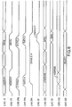
- Figure 8 shows the relative timing of the key signals required to set one of the bit positions of 'SREG 21 (i.e., 2 16 or 217) to a binary one, causing closed loop row or column address return.
- Line 12 contains the data from CPU 10 transferred as an address word and an 8, 16, or 32 bit data word.
- Line 113 shows the presence of the access request and the write command.
- Line 29a indicates timing of the address word cycle, ACYCLE, and the data word cycle, WCYCLE: gating signals are supplied by TIMING AND CONTROL 28 to DMUX 102 via line 29b to gate the address word to AREG 104 (i.e., GATE A) and to gate the data word to DREG 103 (i.e., GATE D).
- TIMING AND CONTROL 28 transfers ENABLE A via line 29c to enable the address determination result (i.e., does AREG 104 contain X77777 8 ) to line 25.
- Lines 120, 121 and 122 conduct the address word and the data word.
- Priority 100 notifies MUX 101 of which of the possible eight interfaces to select via line 126.
- Figure 9a shows the timing of closed loop row address.
- Line 12 contains first the address (see Figure 5a) being transferred to MEMORY 11 from CPU 10 and then ROW ADDRESS (see Figure 5b) being transferred to CPU 10 from MEMORY 11.
- the REQUEST signal is transferred to PRIORITY 100 from DRIVERS AND RECEIVERS 105 via line 112. Signals indicating the address and read cycles are transferred via line 29a.
- Line 29b gates the address as before.
- Line 112 contains the address word during the remaining time.
- Line 32b is low indicating that bit 2 16 of SREG 21 is set (i.e., row address).
- Lines 32c, 32d and 32e are low indicating that bits 2", 2 18 and 2 19 of SREG 21 are clear.
- Line 29d enables DRIVERS AND RECEIVERS 105 to place the data received via line 111 on line 12.
- Line 29e1 is low indicating no access to MEMORY ARRAY 22 is in process.
- Line 29e2 is low indicating row address selection (i.e., bit 2 16 of SREG 21 is set).
- Figure 9b shows the timing of closed loop column address. It is identical to closed loop row address (i.e., Figure 9a) except line 32b is high indicating bit 2 16 of SREG 21 clear, line 32c is low indicating bit 2 17 of SREG 21 set, and line 29e2 is high indicating column address selection (i.e., bit 217 of SREG 21 is set).
Description
- The present invention relates to programmable computers and provides means whereby the memory addressing circuits of the computers may be checked.
- Most present day medium and large scale computers have the capability for the addition or deletion of memory capacity through the addition or deletion of memory modules. These memory modules quite often are operated asynchronously from one another and from other modules (e.g., Central Processing Units, Input/Output Controllers, etc.) within the computer. Furthermore, these memory modules usually have their own addressing circuitry (i.e., holding registers, translators, etc.) to permit ease of interface to other modules within the computer. It is desirable to verify the correct operation of this addressing circuitry. The normal method is to write data into each (or each worst case) addressable location of the memory, read the data, and compare it with what was written. This technique has the advantage of being executed under software control, obviating the need of special test equipment, but it has the disadvantage that the writing and reading of many addressable locations is time consuming, and necessitates relatively large temporary storage capacity to prevent data from being destroyed. Furthermore, the use of addressable locations to test the addressing circuitry may cause errors or ambiguities in the test results if the memory arrays themselves malfunction.
- U.S. Patent Specification Number 3049692 describes a core memory provided with non- programmable means for checking the operation of its address decoder.
- The present invention provides a means whereby the addressing circuits may be tested under programme control without writing into the memory locations and so without the need for displacing data already stored there. To do this, settable means are provided in the memory modules to put them into a maintenance mode. In this mode the memory module responds to a read instruction, not by addressing the specified memory location, but by returning the address, or a portion of it, to the central processor.
- The memory module will normally contain a status register. The contents of the various bit positions of the status register control the operation of the memory module and record status information. One or more bit positions of this register may serve as the settable means for setting up the maintenance mode, which will be referred to herein as "closed loop address".
- In the embodiment to be described, two bit positions of the status register are dedicated to closed loop address. One bit position controls the use of one part of the address, and the second bit position controls the use of the remainder of the address. During normal operation both bit positions are clear (i.e., contain binary zeroes) causing the memory module to use each address instruction received to address the corresponding addressable location within the memory array of the memory module. If either bit is set, the memory module returns a portion of the address received with each read request to the requestor, using the same interface protocol as with a normal read. Two bit positions of the status register are used, and only a part of the address is returned at any one time, because of the manner in which the memory arrays are normally addressed.
- To test the addressing circuitry of the memory module, the CPU, under software control, sets (i.e., causes to contain a binary one) one of the closed loop address bit positions of the status register by writing a binary one into that bit position of the status register. The CPU then presents the memory module with several read requests using various addresses. For each read request, the memory module returns a part of the address as if it were the contents of the addressable location specified by the address. The CPU verifies that the part of the address returned is correct for each read request. The CPU then clears the first bit position of the status register and sets the second bit position of the status register by again writing into the status register. Additional read requests are then generated to verify the correct return of the remainder of the address.
- The invention will now be further described by way of example with reference to the accompanying drawings, in which
- Figure 1 is a schematic block diagram of a computer containing a memory module, showing its major components.
- Figure 2 is a more detailed block diagram of the memory interface circuit.
- Figure 3 is a logic diagram showing the provisions for manual mode change.
- Figure 4 shows the status register and associated circuits.
- Figure 5a shows the format of an address.
- Figure 5b shows the format of a returned row address.
- Figure 5c shows the format of a returned column address.
- Figure 5d is a block diagram showing the operation of the read selection circuits.
- Figure 6 shows the connections of the AND gate circuit.
- Figure 7 is a logic diagram showing the multiplexer enable circuitry.
- Figure 8 is a timing diagram for the operation of writing into the status register.
- Figure 9a is a timing diagram for the return of a closed loop row address.
- Figure 9b is a timing diagram for the return of a closed loop column address.
- The invention will be described in its application to an AN/UYK-7(V) computer set. This is a standard piece of military equipment used by the United States Department of Defence, and is described in the following publications issued by Naval Sea Systems Command in Washington, D.C., from whom copies may be obtained. The publications are, NAVSEA 0967-LP-319-4030; NAVSEA 0967-LP-319-4040; NAVSEA 0967-LP-319-4010 and NAVSEA 0967-LP-319-4020. The first two of these are circuit diagrams for the computer set, and the others are, respectively, a technical description and parts lists.
- Figure 1 is a schematic block diagram of the computer, containing a
memory module 11 employing the present invention. The central processing unit,CPU 10, is programmable through the execution of a series of software instructions as taught by the references cited above.CPU 10 is shown as interfacing to MEMORY 11 vialine 12. - The drawing is simplified for the purpose of describing the present invention, and in fact the interface to
MEMORY 11 is quite complex, and is more fully described in NAVSEA 0967-LP-319-4030. Only one requestor (i.e., CPU 10) is shown, although thememory 11 may have up to eight requestors, as it has eight requestor ports. (See NAVSEA 0967-LP-319-4030). - Interface circuitry, INTERFACE 20, interfaces directly with
CPU 10 vialine 12 and handles the protocol.INTERFACE 20 is shown as transferring data only to status register, SREG 21, vialines CONTROL 28, vialine 29. Actually, INTERFACE 20 also transfers data toMEMORY ARRAY 22 through data paths not shown. - MEMORY ARRAY 22 is a semiconductor random access store constructed using 214 bit monolithic devices such as Motorola MCM4116, MOSTEK MK4116, or National Semiconductor MM5290. MEMORY ARRAY 22 is configured as a 215217 word by 72 bit store. The computer uses a basic 32 bit word without parity, although
CPU 10 may also read into or write fromMEMORY 11 using an eight bit byte or 16 bit half word. Each 72 bit word of MEMORY ARRAY 22 is stored in a group of 72 chips, one bit in each chip, and provides two 32 bit data words and an eight bit error code. Each access (i.e., read from or write into) causes the access of a full 72 bit word from MEMORY ARRAY 22. MEMORY ARRAY 22 is addressed by a word formatted as in Figure 5a. The 18 bit address shown is sufficient to select any one- half word from the possible 217 72-bit words ofMEMORY ARRAY 22. The least significant bit (i.e., 2°) of the address selects the upper or lower half of one 72 bit (i.e., 64 data bits) word of MEMORY ARRAY 22. Bit positions 15, 16 and 17 are designated the ARRAY field. The ARRAY field selects the desired group of chips. Bit positions 1-14 select a given bit on each chip. As those skilled in the art are aware, the referenced devices used in the preferred embodiment have only seven address lines. Therefore, the addressing on each chip is accomplished by supplying first a seven bit ROW ADDRESS followed by a seven bit COLUMN ADDRESS. The impact of this addressing scheme upon the embodiment described herein will become more apparent below. - Referring again to Figure 1, the normal mode change circuitry,
MODE 31, supplies mode change commands to astatus register SREG 21 vialine 27. TIMING ANDCONTROL 28 receives request notification signals fromINTERFACE 20 vialine 29 and supplies timing signals toMEMORY ARRAY 22 vialine 26,INTERFACE 20 vialine 29, andSREG 21 vialine 30. The data path wherebyMEMORY ARRAY 22 supplies read data to INTERFACE 20 is shown asline 24. - Figure 2 provides a more detailed view of
INTERFACE 20. DRIVERS ANDRECEIVERS 105 receive data and control signals fromCPU 10 and transfer data and control signals toCPU 10 vialine 12 which is described by the cited references as the CPU operand memory bus. The cited references also supply circuit descriptions of DRIVERS ANDRECEIVERS 105. The control signals received fromCPU 10 are transferred toPRIORITY 100, which determines when a request received vialine 12 will be honoured. The data received fromCPU 10 vialine 12 are transferred to multiplexer,MUX 101, vialine 110.MUX 101 is necessary becauseMEMORY 11 may interface with up to eight requestors, each with a separate interface to DRIVERS AND RECEIVERS 105 (see NAVSEA 0967-LP-319-4030).PRIORITY 100 determines when any one of the eight requestor ports will be granted access toMEMORY 11.PRIORITY 100 notifiesMUX 101 vialine 126 to select data from one of the eight requestors, only one of which is shownPRIORITY 100 notifies TIMING ANDCONTROL 28 vialine 29a when an access request is to be processed.MUX 101 selects data from one of the eight requestors as specified byPRIORITY 100 vialine 126 and transfers the data to the demultiplexer,DMUX 102, vialine 120.DMUX 102 routes the data to either the data register,DREG 103, vialine 121, or to the address register,AREG 104, vialine 122, based upon a command from TIMING ANDCONTROL 28 received vialine 29b. - The addressing format was explained above. The data word is 8, 16 or 32 bits. Therefore,
DMUX 102 either routes an address word received fromMUX 101 vialine 120 toAREG 104 vialine 122 or routes an 8, 16 or 32 bit data word received fromMUX 101 vialine 120 to DREG 103 vialine 121. The selection is accomplished byDMUX 102 in response to a command from TIMING ANDCONTROL 28 received vialine 29b.AREG 104 is a register which holds the address word received fromDMUZ 102 vialine 122.AREG 104 is normally used to address the memory arrays ofMEMORY 11 via circuitry which is not shown.AREG 104 is also used in accessingSREG 21 through circuitry which is shown.AREG 104 holds the address word. In the preferred embodiment,SREG 21 is accessed using address 77777g (but only ifMEMORY 11 is in MAINTENANCE mode, as explained below). Therefore, to select access to SREG 21 requiresAREG 104 to have bit position 20-214 (i.e., 20, 21, 22, 23, ...., 214) contain binary ones. This provides an address of 77777g. (Note that the address is really X777778 wherein X is determined by address bits 215―217 which are not used to determine access to the status register.) The contents of the 15 bit positions (i.e., 20, 21, 22, 23, ...., 214) are transferred vialines 125 to ANDgate 106. If, and only if, all 15 bit positions contain binary ones (i.e.,AREG 104 contains an address word of X77777$), ANDgate 106 makesline 107 low.Line 107 is high ifAREG 104 contains any other address word. ANDgate 108 makes line 25 a high if and only ifline 29c is high andline 107 is low.Line 29c is a timing signal received from TIMING ANDCONTROL 28. - As stated above,
DREG 103 receives an 8, 16 or 32 bit data word fromDMUX 102 vialine 121.DREG 103 has a number of outputs. The only one relating to the present invention is shown asline 23.Line 23 contains four conductors representing the contents of the four bit positions ofDREG 103 which will be transferred to SREG 21 at those bit positions relating to maintenance routines. In the preferred embodiment they are bit positions 216, 217, 218 and 219. If one of these bit positions contains a binary zero, the corresponding one of the four conductors ofline 23 is at a high. If one of these bit positions contains a binary one, the corresponding one of the four conductors ofline 23 is at a low. -
Line 32 transfers the contents of the status register, including,bits 216, 217, 218 and 2 19 to the read selection circuitry,READ SELECTION 109. Of these, bits 216 and 217 are employed in the present invention, and bits 218 and 219 are concerned with checking of the error correction circuits, as described in our co-pending application no. 79302727.7 filed on the same data as the present invention and claiming priority from U.S. patent application 964 993 (Thorsrud) filed 30 November 1978.Line 33 transfers an enable signal to READSELECTION 109 which is discussed further below.READ SELECTION 109 also receives the contents ofAREG 104 vialine 112.Line 29e providesREAD SELECTION 109 with some required timing signals. DRIVERS ANDRECEIVERS 105 receive an enable from TIMING ANDCONTROL 28 vialine 29d. - Figure 3 is a circuit diagram of the manual mode change circuit,
MODE 31. Single pole- double throw (SPDT)switch 200 is a means whereby an operator enters the mode change.SPDT switch 200 is a momentary contact switch to provide some noise immunity. The use of a momentary contact switch is permissible because a flip-flop, discussed below, stores the actual switch position. Upon being switched to MAINTENANCE mode,SPDT switch 200 momentarily couplesline 220 to ground. NORgate 209 senses this as a low, causing NORgate 209 to makeline 222 high. Assumingline 219 is also high (i.e., no stop signal is present), ANDgate 211 allowsline 224 to be high.Inverter 213 inverts the high and applies a low toline 27a. MAINTENANCE mode may also be entered via automatic means atline 216.Resistors line 220,line 216 andline 224, respectively) to provide desirable rise-times on transitions to high.Capacitor 207 decouples high frequency switching transients. The STOP signal prevents mode change during primary power transients. - A switch to NORMAL mode is accomplished by
SPDT switch 200 being placed into the NORMAL position. The signal is propagated in similar fashion throughNAND gate 210, ANDgate 212 andinverter 214.Pullup resistors inverter 214 applying a low toline 27b.Line 218 provides for return to normal mode in automatic operation. - Figure 4 shows the operation of status register,
SREG 21. Only four bit positions (i.e., bit positions 216, 217, 218 and 219) are illustrated for clarity. The remaining bit positions of SREG 21 provide functions not relevant to the present invention.Line 27a andline 27b transfer the mode change signals (i.e.,line 27a = low + MAINTENANCE mode;line 27b = low NORMAL mode) received fromMODE 31. Flip-flop, F/F 300, actually stores the current mode (i.e., F/F 300 set ⇒MAINTENANCE mode F/F 300 clear ⇒ NORMAL mode). If F/F 300 is set, set output, S, is high. If F/F 300 is clear, S is low. The output of F/F 300 is inverted byinverter 301 and applied togate 302. The output ofgate 302 is high if F/F 300 is set (i.e., MAINTENANCE mode), andline 25 is high (i.e.,AREG 104 contains an address word of X777778 as shown on Figure 2). The output ofgate 302 is inverted byinverter 303 and applied as an input togate 304. During the time whenline 30 from TIMING ANDCONTROL 28 is high and the output ofinverter 303 is low (i.e., output ofgate 302 is high), the output ofgate 304 goes high, which is transferred to the clock input, CLK of the four bit latch 4-BIT LATCH 305 which is a monolithic device of the type 54LS174. Each of the four conductors of line 23 (i.e.,lines DREG 103 contains a binary zero, and is low if the corresponding bit position ofDREG 103 contains a binary one, as explained above. The four INVERTERS (i.e., 306, 307, 308 and 309) invert the signals on the four conductors ofline 23 and provide the inverted signals to 4-BIT LATCH 305 vialines example INVERTER 306 receives a low vialine 23a if bit position 216 ofDREG 103 contains a binary one, and supplies a high to 'input AØ. of 4-BIT LATCH 305. Similarly,INVERTER 307 receives a high vialine 23b if bit positions 2" ofDREG 103 contains a binary zero, and supplies a low to input A1 of 4-BIT LATCH 305. - The outputs of 4-
BIT LATCH 305 are complement outputs at Q0, Q1, Q2 and Q3. That is, if all bit portions of 4-BIT LATCH 305 contain binary zeros, Q0, Q1, Q2 and Q3 are high. If all bit positions of 4-BIT LATCH 305 contain binary ones, Q0, Q1, Q2 and Q3 are low. The state of a bit position of 4-BIT LATCH 305 is changed only when line 304a goes high. When line 304a goes high, the state of the four bit positions of 4-BIT LATCH 305 are determined bylines line 310 is high and line 304a goes high, bit position 216 will be caused to contain a binary one andline 32b will become low. Similarly, ifline 311 is low and line 304a goes high, bit position 217 will be caused to contain a binary zero andline 32c will become high.Lines line 32a. - As explained above Figure 5a shows the format of the address word received by
MEMORY 11. As also explained earlier,MEMORY ARRAY 22 requires presentation of a seen bit row address along with the three bits to select the chip group (i.e., ARRAY field) followed by presentation of a seven bit column address along with the ARRAY field. For that reason two closed loop address modes are defined. Figure 5b shows the format of the closed loop row address returned to CPU if bit 216 of the status
CPU 10 if bit 217 of the status register is set. The mode wherein both bits 216 and 217 are set is undefined and will not be discussed further. - Figure 5d shows the details of read selection circuitry,
READ SELECTION 109. Four multiplexers are shown (i.e.,AMUX 400,EMUX 401,RMUX 404 and SMUX 402). The standard monolithic part 54LS158 is used which provides selection of one of two groups of four signals. Each of the four multiplexers shown uses as many 54LS158 devices as required for the number of signals to be handled. Each of the four multiplexers has inputs from two data streams, an output of one data stream, a selector, and an enable. Table B shows the connections to each multiplexer. The grounded enable causes the devices to be enabled at all times. The multiplexer enable circuitry, MUXEN .403 provides control signals to EMUX 401,RMUX 418 andSMUX 402.AGATE 405 "ANDs" the two data streams fromline line 111. -
AMUX 400 selects row or column address formats.AMUX 400 is presented with an address of the format shown in Figure 5a with bit 20 (U/L) online 112a, bits 21―27 (row address) online 112b, bits 28_214 (column address) online 112c, and bits 215―217 (ARRAY field) ontine 112d.AMUX 400 places a row address (see Figure 5b) online 410 if line 29e2 from TIMING ANDCONTROL 28 is low, and places a column address (see Figure 5c) online 410 if line 29e2 from TIMING ANDCONTROL 28 is high. The selection of row address or column address based upon the state of line 29e2 is dynamic (i.e., line 29e2 changes state) during a normal access ofMEMORY ARRAY 22. This circuitry is not shown, however, as
SREG 21 is set and high if bit position 217 ofSREG 21 is set. (Note that both bits clear is normal access ofMEMORY ARRAY 22 and both bits set is undefined.) -
EMUX 401 receives the eight bit error log data vialine 411 or the address (row or column) data vialine 410 and selects one or the other for transfer to SMUX 402 vialine 413 based upon the state ofline 412 fromMUXEN 403. Ifline 412 is high, the error log data is selected. This mode is used in our co-pending application referred to above. Ifline 412 is low the address data is selected. If the eight bit error log data is selected, the remaining three bits transferred via the 11 -bit line 413 are binary ones. The circuitry determining the state ofline 412 is explained below. -
SMUX 402 selects either the 32-bit contents ofSREG 21 received vialine 32 or the 11-bit word received vialine 413 based upon the state ofline 33. Ifline 33 is low,SMUX 402 selects the 32-bit contents ofSREG 21. Ifline 33 is high,SMUX 402 selects the 11-bit word received vialine 413. The state ofline 33 is determined as explained above by AND gate 302 (see Figure 4).Line 416 is connected to the enable ofSMUX 402. Ifline 416 is low,SMUX 402 is enabled for output. Ifline 416 is high,SMUX 402 is disabled and all 32 conductors ofline 415 are high. Ifline 33 is high and the 11-bit word received vialine 413 is selected, bits 2" to 23i are high (see also Figures 5b and 5c). -
RMUX 404 is used to perform the upper/lower selection based upon bit 2° of the address word. Line 24a andline 24b transfer the upper and lower 32 bits respectively.Line 112a transfers bit 2° of the address word.Inverter 406 inverts the state of line 1 12a and applies it vialine 419 to the selection input ofRMUX 404.Line 418 is the enable input to RMUX 404 received fromMUXEN 403. Ifline 418 is low,RMUX 404 transfers the upper or lower 32 bits received vialines 24a and 24b, respectively as selected byline 419 toline 417. Ifline 418 is high,RMUX 404 makes all 32 conductors ofline 417 high. - Figure 6 shows the circuitry in
AGATE 405. The AND gates 500-531 combine the two 32-bit data streams received fromlines 415 and 517 into a single 32-bit data stream which is transferred to DRIVERS ANDRECEIVERS 105 vialine 111. As explained below,SMUX 402 and RMUX 404 cannot both be enabled simultaneously. Therefore, all 32 conductors of eitherline 415 orline 417 must be all ones. - Figure 7 shows the circuitry of
MUXEN 403.Line 412 is high, selecting error log data, (see also Figure 5d) atEMUX 401 ifline 32e is low andline 33a is low.Line 412 is high, selecting address data, if eitherline 32e or line 33al is high.Line 32c is low if bit 219 is set in SREG 21 (see Figure 4) andline 33a (i.e., 33 and 33a) is low ifSREG 21 is not being addressed (also see Figure 4). -
Line 416 enablesSMUX 402 if it is low and disablesSMUX 402 if it is high. ORgate 605 makesline 416 low (enables SMUX 402) if line 33a2 is low (i.e.,SREG 21 is not being addressed as explained above) or ifline 32e is low (i.e., bit 219 ofSREG 21 is set) or if either bit 216 (row address) or bits 217 (column address) is set andSREG 21 is not being addressed (i.e., line 33a4 is low). -
Line 418 is low enabling RMUX 404 if the error log data has not been selected by EMUX 401 (i.e.,line 412 is low) and either TIMING ANDCONTROL 28 makes line 29e1 high, signifying a read fromMEMORY ARRAY 22, or bit 218 ofSREG 21 is set andSREG 21 is not being addressed. The illustration ofRMUX 404 and associated circuitry is shown for completeness and not because of its necessity to the present invention. The logic devices used to implement the present invention are all common Schottky or low power Schottky devices. - Figure 8 shows the relative timing of the key signals required to set one of the bit positions of 'SREG 21 (i.e., 216 or 217) to a binary one, causing closed loop row or column address return.
Line 12 contains the data fromCPU 10 transferred as an address word and an 8, 16, or 32 bit data word.Line 113 shows the presence of the access request and the write command.Line 29a indicates timing of the address word cycle, ACYCLE, and the data word cycle, WCYCLE: gating signals are supplied by TIMING ANDCONTROL 28 to DMUX 102 vialine 29b to gate the address word to AREG 104 (i.e., GATE A) and to gate the data word to DREG 103 (i.e., GATE D). TIMING ANDCONTROL 28 transfers ENABLE A vialine 29c to enable the address determination result (i.e., doesAREG 104 contain X777778) toline 25.Lines Priority 100 notifiesMUX 101 of which of the possible eight interfaces to select vialine 126. - Figure 9a shows the timing of closed loop row address.
Line 12 contains first the address (see Figure 5a) being transferred toMEMORY 11 fromCPU 10 and then ROW ADDRESS (see Figure 5b) being transferred toCPU 10 fromMEMORY 11. The REQUEST signal is transferred toPRIORITY 100 from DRIVERS ANDRECEIVERS 105 vialine 112. Signals indicating the address and read cycles are transferred vialine 29a.Line 29b gates the address as before.Line 112 contains the address word during the remaining time.Line 32b is low indicating that bit 216 ofSREG 21 is set (i.e., row address).Lines SREG 21 are clear.Line 29d enables DRIVERS ANDRECEIVERS 105 to place the data received vialine 111 online 12. Line 29e1 is low indicating no access toMEMORY ARRAY 22 is in process. Line 29e2 is low indicating row address selection (i.e., bit 216 ofSREG 21 is set). - Figure 9b shows the timing of closed loop column address. It is identical to closed loop row address (i.e., Figure 9a) except
line 32b is high indicating bit 216 of SREG 21 clear,line 32c is low indicating bit 217 of SREG 21 set, and line 29e2 is high indicating column address selection (i.e.,bit 217 ofSREG 21 is set).
Claims (4)
Applications Claiming Priority (2)
| Application Number | Priority Date | Filing Date | Title |
|---|---|---|---|
| US05/964,992 US4227244A (en) | 1978-11-30 | 1978-11-30 | Closed loop address |
| US964992 | 1978-11-30 |
Publications (2)
| Publication Number | Publication Date |
|---|---|
| EP0012018A1 EP0012018A1 (en) | 1980-06-11 |
| EP0012018B1 true EP0012018B1 (en) | 1982-04-21 |
Family
ID=25509283
Family Applications (1)
| Application Number | Title | Priority Date | Filing Date |
|---|---|---|---|
| EP79302728A Expired EP0012018B1 (en) | 1978-11-30 | 1979-11-29 | Checking the memory addressing circuits of computers |
Country Status (4)
| Country | Link |
|---|---|
| US (1) | US4227244A (en) |
| EP (1) | EP0012018B1 (en) |
| JP (1) | JPS6034145B2 (en) |
| DE (1) | DE2962592D1 (en) |
Families Citing this family (10)
| Publication number | Priority date | Publication date | Assignee | Title |
|---|---|---|---|---|
| US4334307A (en) * | 1979-12-28 | 1982-06-08 | Honeywell Information Systems Inc. | Data processing system with self testing and configuration mapping capability |
| US4385349A (en) * | 1980-11-20 | 1983-05-24 | International Business Machines Corporation | Central processor supervised controller system having a simulation of the controller in the central processor for test purposes |
| US4449182A (en) * | 1981-10-05 | 1984-05-15 | Digital Equipment Corporation | Interface between a pair of processors, such as host and peripheral-controlling processors in data processing systems |
| US4608669A (en) * | 1984-05-18 | 1986-08-26 | International Business Machines Corporation | Self contained array timing |
| US4726023A (en) * | 1986-05-14 | 1988-02-16 | International Business Machines Corporation | Determination of testability of combined logic end memory by ignoring memory |
| FR2629248B1 (en) * | 1988-03-25 | 1992-04-24 | Sgs Thomson Microelectronics | SINGLE PROGRAMMING MEMORY TESTING METHOD AND CORRESPONDING MEMORY |
| US5231640A (en) * | 1990-07-20 | 1993-07-27 | Unisys Corporation | Fault tolerant processor/memory architecture |
| JP2549209B2 (en) * | 1991-01-23 | 1996-10-30 | 株式会社東芝 | Semiconductor memory device |
| GB9417266D0 (en) * | 1994-08-26 | 1994-10-19 | Inmos Ltd | Testing a non-volatile memory |
| US7234099B2 (en) * | 2003-04-14 | 2007-06-19 | International Business Machines Corporation | High reliability memory module with a fault tolerant address and command bus |
Family Cites Families (7)
| Publication number | Priority date | Publication date | Assignee | Title |
|---|---|---|---|---|
| US3049692A (en) * | 1957-07-15 | 1962-08-14 | Ibm | Error detection circuit |
| US3270318A (en) * | 1961-03-27 | 1966-08-30 | Sperry Rand Corp | Address checking device |
| GB948519A (en) * | 1961-11-10 | 1964-02-05 | Ass Elect Ind | Improvements relating to arrangements for detecting signal transmission errors in telegraph and like systems |
| US3665175A (en) * | 1968-09-03 | 1972-05-23 | Ibm | Dynamic storage address blocking to achieve error toleration in the addressing circuitry |
| DE2209253A1 (en) * | 1972-02-26 | 1973-09-06 | Ibm Deutschland | PROCEDURE AND CIRCUIT ARRANGEMENT FOR ERROR CHECKING A MEMORY ADDRESSING |
| DE2423260A1 (en) * | 1974-05-14 | 1975-11-20 | Siemens Ag | PROCEDURE AND CIRCUIT ARRANGEMENT FOR TESTING DATA PROCESSING SYSTEMS, IN PARTICULAR TELEVISION SYSTEMS WITH PERIPHERAL EQUIPMENT CONNECTED TO A CONTROL CENTER via a BUS SYSTEM |
| US3982111A (en) * | 1975-08-04 | 1976-09-21 | Bell Telephone Laboratories, Incorporated | Memory diagnostic arrangement |
-
1978
- 1978-11-30 US US05/964,992 patent/US4227244A/en not_active Expired - Lifetime
-
1979
- 1979-11-29 EP EP79302728A patent/EP0012018B1/en not_active Expired
- 1979-11-29 DE DE7979302728T patent/DE2962592D1/en not_active Expired
- 1979-11-30 JP JP54156300A patent/JPS6034145B2/en not_active Expired
Also Published As
| Publication number | Publication date |
|---|---|
| JPS5577100A (en) | 1980-06-10 |
| US4227244A (en) | 1980-10-07 |
| EP0012018A1 (en) | 1980-06-11 |
| JPS6034145B2 (en) | 1985-08-07 |
| DE2962592D1 (en) | 1982-06-03 |
Similar Documents
| Publication | Publication Date | Title |
|---|---|---|
| US3979726A (en) | Apparatus for selectively clearing a cache store in a processor having segmentation and paging | |
| EP0076629B1 (en) | Reconfigureable memory system | |
| US4084236A (en) | Error detection and correction capability for a memory system | |
| EP0012017B1 (en) | Programmable computer comprising means for checking the error-correcting circuits | |
| US5537665A (en) | Multiple bank column redundancy intialization controller for cache RAM | |
| US4617624A (en) | Multiple configuration memory circuit | |
| EP0336435B1 (en) | Memory diagnostic apparatus and method | |
| US3579199A (en) | Method and apparatus for fault testing a digital computer memory | |
| US4404647A (en) | Dynamic array error recovery | |
| US3815103A (en) | Memory presence checking apparatus | |
| GB1573539A (en) | Digital data processing apparatus | |
| JPS6349319B2 (en) | ||
| EP0012018B1 (en) | Checking the memory addressing circuits of computers | |
| US3866182A (en) | System for transferring information between memory banks | |
| GB1277902A (en) | Data processing systems | |
| US4809276A (en) | Memory failure detection apparatus | |
| WO1982002266A1 (en) | Method and apparatus for detecting and correcting errors in a memory | |
| US4796222A (en) | Memory structure for nonsequential storage of block bytes in multi-bit chips | |
| US4962501A (en) | Bus data transmission verification system | |
| EP0549218B1 (en) | A memory apparatus and method for use in a data processing system | |
| US3840864A (en) | Multiple memory unit controller | |
| US4992979A (en) | Memory structure for nonsequential storage of block bytes in multi bit chips | |
| CA2005698A1 (en) | Programmable option selection and paged memory cache coherency control | |
| US4811266A (en) | Multifunction arithmetic indicator | |
| WO1981001208A1 (en) | Data processor having common monitoring and memory loading and checking means |
Legal Events
| Date | Code | Title | Description |
|---|---|---|---|
| PUAI | Public reference made under article 153(3) epc to a published international application that has entered the european phase |
Free format text: ORIGINAL CODE: 0009012 |
|
| AK | Designated contracting states |
Designated state(s): DE FR GB IT |
|
| 17P | Request for examination filed | ||
| ITF | It: translation for a ep patent filed |
Owner name: ING. C. GREGORJ S.P.A. |
|
| GRAA | (expected) grant |
Free format text: ORIGINAL CODE: 0009210 |
|
| AK | Designated contracting states |
Designated state(s): DE FR GB IT |
|
| REF | Corresponds to: |
Ref document number: 2962592 Country of ref document: DE Date of ref document: 19820603 |
|
| PGFP | Annual fee paid to national office [announced via postgrant information from national office to epo] |
Ref country code: FR Payment date: 19921111 Year of fee payment: 14 |
|
| ITTA | It: last paid annual fee | ||
| PG25 | Lapsed in a contracting state [announced via postgrant information from national office to epo] |
Ref country code: FR Effective date: 19940729 |
|
| REG | Reference to a national code |
Ref country code: FR Ref legal event code: ST |
|
| PGFP | Annual fee paid to national office [announced via postgrant information from national office to epo] |
Ref country code: GB Payment date: 19941017 Year of fee payment: 16 |
|
| PGFP | Annual fee paid to national office [announced via postgrant information from national office to epo] |
Ref country code: DE Payment date: 19941130 Year of fee payment: 16 |
|
| PG25 | Lapsed in a contracting state [announced via postgrant information from national office to epo] |
Ref country code: GB Effective date: 19951129 |
|
| GBPC | Gb: european patent ceased through non-payment of renewal fee |
Effective date: 19951129 |
|
| PG25 | Lapsed in a contracting state [announced via postgrant information from national office to epo] |
Ref country code: DE Effective date: 19960801 |
|
| PLBE | No opposition filed within time limit |
Free format text: ORIGINAL CODE: 0009261 |
|
| STAA | Information on the status of an ep patent application or granted ep patent |
Free format text: STATUS: NO OPPOSITION FILED WITHIN TIME LIMIT |