EP0010882B1 - A switching circuit - Google Patents
A switching circuit Download PDFInfo
- Publication number
- EP0010882B1 EP0010882B1 EP79302162A EP79302162A EP0010882B1 EP 0010882 B1 EP0010882 B1 EP 0010882B1 EP 79302162 A EP79302162 A EP 79302162A EP 79302162 A EP79302162 A EP 79302162A EP 0010882 B1 EP0010882 B1 EP 0010882B1
- Authority
- EP
- European Patent Office
- Prior art keywords
- switch
- circuit
- fault
- load
- logic
- Prior art date
- Legal status (The legal status is an assumption and is not a legal conclusion. Google has not performed a legal analysis and makes no representation as to the accuracy of the status listed.)
- Expired
Links
- 239000007787 solid Substances 0.000 claims abstract description 4
- 239000003990 capacitor Substances 0.000 description 4
- 230000005540 biological transmission Effects 0.000 description 2
- 230000003111 delayed effect Effects 0.000 description 2
- 230000001419 dependent effect Effects 0.000 description 2
- 230000000295 complement effect Effects 0.000 description 1
- 238000010586 diagram Methods 0.000 description 1
- 230000001771 impaired effect Effects 0.000 description 1
- WFKWXMTUELFFGS-UHFFFAOYSA-N tungsten Chemical compound [W] WFKWXMTUELFFGS-UHFFFAOYSA-N 0.000 description 1
- 229910052721 tungsten Inorganic materials 0.000 description 1
- 239000010937 tungsten Substances 0.000 description 1
Images
Classifications
-
- H—ELECTRICITY
- H03—ELECTRONIC CIRCUITRY
- H03K—PULSE TECHNIQUE
- H03K17/00—Electronic switching or gating, i.e. not by contact-making and –breaking
- H03K17/08—Modifications for protecting switching circuit against overcurrent or overvoltage
- H03K17/082—Modifications for protecting switching circuit against overcurrent or overvoltage by feedback from the output to the control circuit
- H03K17/0826—Modifications for protecting switching circuit against overcurrent or overvoltage by feedback from the output to the control circuit in bipolar transistor switches
Definitions
- This invention relates to a switching circuit according to the first part of claim 1, which is known from US-A-3 906 258.
- a switching circuit comprising a solid state switch, switching power to a load drive circuitry for driving the switch, sensing circuitry for sensing an operating characteristic of the switch characterised in that the sensing circuitry comprises three individual circuitry each of which is set to indicate whether the operating characteristic sensed is greater or less than a given threshold value for that individual sensing circuit, and digital logic circuit means (5, 6, 8) operative to produce two digital output signals from the signals received from the sensing circuitry, one of the two signals indicating whether a fault in the switch or in the load, which in operation of the circuit is fed from the switch, is present or not and the other signal indicating whether that fault is serious or not.
- a preferred embodiment of the invention may comprise any of the following advantageous features:-
- the status of the power switch and the current in the load is sensed by the magnitude of the emitter-collector voltage in saturation (VECSAT).
- the sensing circuitry comprises three individual sensing circuits. If the current in the load is zero, then VECSAT is also approximately zero. If the normal current flows in the load then VECSAT is usually between 0.8 and 1.5 volts. If the load is short circuited, then VECSAT is obviously equal to the full rail voltage. If a partial short circuit load condition arises, or alternatively if the power transistor is faulty, an abnormally high VECSAT, say greater than three volts, will occur.
- the output of each of the three circuits of the sensing circuitry is either 0 or 1 depending upon whether VECSAT is greater or less than a given threshold voltage which is set at different values in each of the three circuits.
- the threshold value of the first circuit is set at 0.7 volts
- the threshold value of the second value of VECSAT which will depend on the characteristic of the power transistor and the size of the load.
- the third circuit has a threshold value at the rail voltage less than 0.7 volts.
- the three circuits are conceived in such a way that a current is supplied to the load when the power supply is off, and different combinations of the three digital logic output levels of the three circuits occur if faults in the switch or in the load, or a normal condition are present.
- a circuit 1 comprises an input 15, output 16, two resistors 13 and 14, two transistors 11 and 12 and power transistor means (9, 10) connected to perform the function of a power switch.
- Current is supplied to a load L from the output 16 through to ground, when the input 15 is high. If the input 15 is low then the power transistor 9 is off and cannot supply current to the load.
- Transistor 10 serves merely to provide sufficient base current to drive the power transistor 9, and transistor 12 similarly provides base current to drive the transistor 10.
- the presence of transistor 11 is to provide the load for transistor 12.
- the current consumed by the switch when off, is limited by the value of resistor 13 which can have a high value. If a typical power transistor such as TIP 3055 is used for transistor 9, the value of VECSAT depends on the load resistor and hence the load current as shown in the following table 1.
- a further circuit 2 contains a resistor 18 and a transistor 20 connected such that a digital output level at output A is high (logic 1) if the input which is connected to the emitter of the power transistor 9 (terminal 16) is within 0.7V approximately of the positive power rail 17. Transistor 20 is therefore used as a switch with a threshold of 0.7V.
- a circuit 4 similarly provides a digital logic output at E dependent upon the voltage at the input which is connected to the emitter of the power transistor 9.
- This circuit 4 comprises two transistors 22 and 26, a resistor 23 connected to the transistor 22 base, a resistor 24 connected to the transistor 22 collector, a zener diode 21 connected to the transistor 22 emitter, a resistor 25 connecting the collector of transistor 22 and base of transistor 26 and a resistor 27 connected to the collector of transistor 26.
- the threshold value for the input to circuit 4 is dependent upon the zener voltage of diode 21 summed with the threshold of transistor 22 which is approximately 0.7V.
- Transistor 26 simply provides an appropriate logic level for the output E at 12V when high, and approximately zero volts when low.
- a suitable value for the zener voltage of diode 21 would be 4.7V, in which case the output E would be high if VECSAT was less than 5.4V, alternately the output E would be low if VECSAT was greater than 5.4V.
- a circuit 3, is simply the complement of circuit 2, and a high digital output is obtained at output B of circuit 3 if VECSAT rises to within 0.7V of the rail voltage, alternately a low state for output B is obtained.
- Circuit 3 comprises a transistor 30 having a base resistor 29 and collector resistor 28. The inputs to the three circuits 2, 3 and 4 are all connected together with the following result. If the power transistor 9 is off and the load connected, then resistors 18 and 23 feed current through the load enabling its continuity to be tested. If the load is open circuit and transistor 9 is off then transistors 20 and 30 are biased on. The value of resistors 29, 23 and 18 are chosen so that, in this condition, transistor 22 is also biased on.
- the two inputs of an exclusive OR gate 31 are respectively connected to outputs A and B and produce from the signals presented at its inputs a digital output signal Z.
- the logic circuit 5 has digital inputs E, Z, V ln and B and produces a logic output P which can be expressed in Boolean algebra as
- the logic circuit 6 has digital inputs A, E, Z and V in and produces a logic output Q. This can be expressed as
- Q is low for serious faults, otherwise it is high. If P is high indicating a no fault condition, then Q is low, but at any rate the value of Q is irrelevant if no fault exists.
- Table 2 expresses the relationship between all the digital signals appropriate to the condition of the load and power transistor 9.
- Circuit 7 contains gating means to disable the switch by isolating input 15 to the switch circuit 1 from V in , which is applied at terminal 32, providing both P and Q are low together indicating a serious fault is present. This obviates the normal requirements to fuse the switch. For any other condition of P together with Q, the inverse of V in appears at terminal 15.
- a time constant made up of resistor 33 and capacitor 34 is inserted in order that the disabling signal is delayed. This is done so that initial surges of current when filament bulbs, for example, are first switched on, do not cause the switch circuit 1 to be turned off.
- the initial surge of current into the tungsten filament bulb may constitute a short circuit load condition for a short period of time which may be typical of the order of 30ms for a 22W bulb.
- the time constant obtained by the product of resistor 33 and capacitor 34 must therefore exist to enable the initial surge of current to occur.
- a low pass filter circuit comprising a resistor 35 and capacitor 37 is included in order that high frequency variations of the positive power rail 17 are not transmitted to the positive terminal V cc , of all the logic gates.
- the transistors 22 and 26 are also fed from the low pass filter comprising resistor 35 and capacitor 37. This filter prevents the system from oscillating when a short circuit load condition arises. If a filter were not present, then on the occurrence of a short circuit load the value of the voltage on the positive rail 17 may fall to such a low value, that the switch is disabled and the logic circuits do not function correctly such that the entire system can oscillate without the switch 1 being disabled by the circuit 7.
- Logic circuit 8 is supplied with logic inputs Q and P together with a square wave signal S from source M which alternately provides a logic 1 followed by a logic 0 sequentially in time.
- the logic output produced by the circuit at D provides information as to the presence of a fault when taken in association with S which is compared with Q by an exclusive OR gate 38.
- Signals S and D are, therefore appropriate signals for the sequential transmission of information regarding the presence or not of a fault and the type of fault if appropriate, by a multiplex transmission system.
- the truth table applicable to the logic produced by circuit 8 is set out in table 3 below.
Landscapes
- Electronic Switches (AREA)
Abstract
Description
- This invention relates to a switching circuit according to the first part of
claim 1, which is known from US-A-3 906 258. - In the event of a fault, either in the switch itself or in the load, the current through the switch will be greater than it should be. This change in the current operating characteristic of the switch can be monitored and used to indicate that a fault is present and that corrective action needs to be taken. Corrective action then taken can avoid further damage to the switch, and perhaps more important to the load itself.
- Switching circuitry of this general type is already known. U.S. Patent No. 3,950,656 to Sumida and U.S. Patent No. 3,906,258 to Moe each disclose circuitry in which a solid state switch is provided with sensing circuitry which enables an operating characteristic of the switch to be sensed. A control signal can then be produced in dependence upon the sensed operating characteristic. The circuitry of neither of these two U.S. Patents, however, provides for action to be taken in dependence upon the sensing of a serious as opposed to a non-serious fault. Such a facility is of great importance in multiplex information handling systems for vehicles for it enables provision to be made for the system to be shut down only when serious further damage may result if it is not or when safety may be impaired by the fault. Conversely, of course, in the case of a non-serious fault it is advantageous to be able to avoid having to shut down the system and thereby immobilise the vehicle with all the attendant inconvenience. An object of the present invention is therefore to provide this facility.
- According to the present invention, there is provided a switching circuit comprising a solid state switch, switching power to a load drive circuitry for driving the switch, sensing circuitry for sensing an operating characteristic of the switch characterised in that the sensing circuitry comprises three individual circuitry each of which is set to indicate whether the operating characteristic sensed is greater or less than a given threshold value for that individual sensing circuit, and digital logic circuit means (5, 6, 8) operative to produce two digital output signals from the signals received from the sensing circuitry, one of the two signals indicating whether a fault in the switch or in the load, which in operation of the circuit is fed from the switch, is present or not and the other signal indicating whether that fault is serious or not.
- A preferred embodiment of the invention may comprise any of the following advantageous features:-
- (a) Logic circuitry is provided to disable the switch if a serious fault exists, and
- (b) The logic circuitry of (a) incorporates means for delaying the application of a disabling signal.
- In a preferred way of carrying out the invention employing a bipolar power transistor as a switch applying a load, the status of the power switch and the current in the load is sensed by the magnitude of the emitter-collector voltage in saturation (VECSAT). The sensing circuitry comprises three individual sensing circuits. If the current in the load is zero, then VECSAT is also approximately zero. If the normal current flows in the load then VECSAT is usually between 0.8 and 1.5 volts. If the load is short circuited, then VECSAT is obviously equal to the full rail voltage. If a partial short circuit load condition arises, or alternatively if the power transistor is faulty, an abnormally high VECSAT, say greater than three volts, will occur.
- The output of each of the three circuits of the sensing circuitry is either 0 or 1 depending upon whether VECSAT is greater or less than a given threshold voltage which is set at different values in each of the three circuits. The threshold value of the first circuit is set at 0.7 volts, the threshold value of the second value of VECSAT, which will depend on the characteristic of the power transistor and the size of the load. The third circuit has a threshold value at the rail voltage less than 0.7 volts. The three circuits are conceived in such a way that a current is supplied to the load when the power supply is off, and different combinations of the three digital logic output levels of the three circuits occur if faults in the switch or in the load, or a normal condition are present.
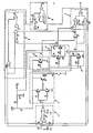
- In order that the invention may be more clearly understood, one embodiment thereof will now be described, by way of example, with reference to the accompanying drawing, which shows a circuit diagram of an electronic power switch with diagnostics for a vehicle.
- Referring to the drawing, a
circuit 1, comprises an input 15,output 16, tworesistors transistors 11 and 12 and power transistor means (9, 10) connected to perform the function of a power switch. Current is supplied to a load L from theoutput 16 through to ground, when the input 15 is high. If the input 15 is low then the power transistor 9 is off and cannot supply current to the load.Transistor 10 serves merely to provide sufficient base current to drive the power transistor 9, andtransistor 12 similarly provides base current to drive thetransistor 10. The presence of transistor 11 is to provide the load fortransistor 12. The current consumed by the switch when off, is limited by the value ofresistor 13 which can have a high value. If a typical power transistor such as TIP 3055 is used for transistor 9, the value of VECSAT depends on the load resistor and hence the load current as shown in the following table 1.
- A further circuit 2, contains a resistor 18 and a transistor 20 connected such that a digital output level at output A is high (logic 1) if the input which is connected to the emitter of the power transistor 9 (terminal 16) is within 0.7V approximately of the
positive power rail 17. Transistor 20 is therefore used as a switch with a threshold of 0.7V. A circuit 4 similarly provides a digital logic output at E dependent upon the voltage at the input which is connected to the emitter of the power transistor 9. This circuit 4 comprises twotransistors 22 and 26, aresistor 23 connected to thetransistor 22 base, a resistor 24 connected to thetransistor 22 collector, azener diode 21 connected to thetransistor 22 emitter, aresistor 25 connecting the collector oftransistor 22 and base of transistor 26 and aresistor 27 connected to the collector of transistor 26. The threshold value for the input to circuit 4 is dependent upon the zener voltage ofdiode 21 summed with the threshold oftransistor 22 which is approximately 0.7V. Transistor 26 simply provides an appropriate logic level for the output E at 12V when high, and approximately zero volts when low. A suitable value for the zener voltage ofdiode 21 would be 4.7V, in which case the output E would be high if VECSAT was less than 5.4V, alternately the output E would be low if VECSAT was greater than 5.4V. A circuit 3, is simply the complement of circuit 2, and a high digital output is obtained at output B of circuit 3 if VECSAT rises to within 0.7V of the rail voltage, alternately a low state for output B is obtained. Circuit 3 comprises atransistor 30 having abase resistor 29 andcollector resistor 28. The inputs to the three circuits 2, 3 and 4 are all connected together with the following result. If the power transistor 9 is off and the load connected, thenresistors 18 and 23 feed current through the load enabling its continuity to be tested. If the load is open circuit and transistor 9 is off thentransistors 20 and 30 are biased on. The value ofresistors transistor 22 is also biased on. - The two inputs of an
exclusive OR gate 31 are respectively connected to outputs A and B and produce from the signals presented at its inputs a digital output signal Z. - There are three
logic circuits logic circuit 5 has digital inputs E, Z, Vln and B and produces a logic output P which can be expressed in Boolean algebra as - P = B when Vin = 1 (the off condition of switch)
or - P = Z . E when Vin = 0 (the on condition of switch)
- If P is low there is a fault condition, otherwise P is high.
- The logic circuit 6 has digital inputs A, E, Z and Vin and produces a logic output Q. This can be expressed as
- Q = Z·
E when Vin = 1 (the off condition of switch)
or - Q =
A when Vin = 0 (the on condition of switch) - Providing a fault exists, Q is low for serious faults, otherwise it is high. If P is high indicating a no fault condition, then Q is low, but at any rate the value of Q is irrelevant if no fault exists. The following table 2 expresses the relationship between all the digital signals appropriate to the condition of the load and power transistor 9.

- Circuit 7 contains gating means to disable the switch by isolating input 15 to the
switch circuit 1 from Vin, which is applied atterminal 32, providing both P and Q are low together indicating a serious fault is present. This obviates the normal requirements to fuse the switch. For any other condition of P together with Q, the inverse of Vin appears at terminal 15. A time constant made up ofresistor 33 andcapacitor 34 is inserted in order that the disabling signal is delayed. This is done so that initial surges of current when filament bulbs, for example, are first switched on, do not cause theswitch circuit 1 to be turned off. The initial surge of current into the tungsten filament bulb may constitute a short circuit load condition for a short period of time which may be typical of the order of 30ms for a 22W bulb. The time constant obtained by the product ofresistor 33 andcapacitor 34 must therefore exist to enable the initial surge of current to occur. - A low pass filter circuit comprising a
resistor 35 andcapacitor 37 is included in order that high frequency variations of thepositive power rail 17 are not transmitted to the positive terminal Vcc, of all the logic gates. Thetransistors 22 and 26 are also fed from the low passfilter comprising resistor 35 andcapacitor 37. This filter prevents the system from oscillating when a short circuit load condition arises. If a filter were not present, then on the occurrence of a short circuit load the value of the voltage on thepositive rail 17 may fall to such a low value, that the switch is disabled and the logic circuits do not function correctly such that the entire system can oscillate without theswitch 1 being disabled by the circuit 7. -
Logic circuit 8 is supplied with logic inputs Q and P together with a square wave signal S from source M which alternately provides alogic 1 followed by a logic 0 sequentially in time. The logic output produced by the circuit at D provides information as to the presence of a fault when taken in association with S which is compared with Q by an exclusive ORgate 38. Signals S and D are, therefore appropriate signals for the sequential transmission of information regarding the presence or not of a fault and the type of fault if appropriate, by a multiplex transmission system. The logic can be stated as follows: if S = Q then set D = P, if S * Q then set D = 1. The truth table applicable to the logic produced bycircuit 8 is set out in table 3 below.
- It will be appreciated that the above embodiment has been described by way of example only. Instead of delaying acting upon a fault signal produced during initial switch on condition of a filament bulb, the fault signal can be accepted immediately but action normally consequent upon it to switch off the bulb will be delayed.
Claims (3)
Priority Applications (1)
| Application Number | Priority Date | Filing Date | Title |
|---|---|---|---|
| AT79302162T ATE4947T1 (en) | 1978-10-21 | 1979-10-10 | CIRCUIT. |
Applications Claiming Priority (2)
| Application Number | Priority Date | Filing Date | Title |
|---|---|---|---|
| GB7841475 | 1978-10-21 | ||
| GB4147578 | 1978-10-21 |
Publications (2)
| Publication Number | Publication Date |
|---|---|
| EP0010882A1 EP0010882A1 (en) | 1980-05-14 |
| EP0010882B1 true EP0010882B1 (en) | 1983-10-05 |
Family
ID=10500504
Family Applications (1)
| Application Number | Title | Priority Date | Filing Date |
|---|---|---|---|
| EP79302162A Expired EP0010882B1 (en) | 1978-10-21 | 1979-10-10 | A switching circuit |
Country Status (5)
| Country | Link |
|---|---|
| US (1) | US4441136A (en) |
| EP (1) | EP0010882B1 (en) |
| JP (1) | JPS5580917A (en) |
| AT (1) | ATE4947T1 (en) |
| DE (1) | DE2966268D1 (en) |
Families Citing this family (34)
| Publication number | Priority date | Publication date | Assignee | Title |
|---|---|---|---|---|
| US4375073A (en) * | 1980-06-16 | 1983-02-22 | Reliance Electric Company | Dual-monitoring protection circuit for switching transistor |
| FR2517067A1 (en) * | 1981-11-25 | 1983-05-27 | Renault Vehicules Ind | CONTROL, SAFETY AND DIAGNOSTIC DEVICE FOR VEHICLE ELECTRIC CIRCUIT |
| US4547828A (en) * | 1983-05-31 | 1985-10-15 | General Electric Company | Circuit for preventing excessive power dissipation in power switching semiconductors |
| US4628397A (en) * | 1984-06-04 | 1986-12-09 | General Electric Co. | Protected input/output circuitry for a programmable controller |
| FR2582879A1 (en) * | 1985-06-04 | 1986-12-05 | Telemecanique Electrique | STATIC SWITCHING APPARATUS OR CIRCUIT FOR PROTECTED POWER SUPPLY OF A LOAD AND ITS LINE |
| GB2183853B (en) * | 1985-12-02 | 1989-12-20 | Trw Inc | Power supply switch circuit for wafer scale applications |
| DE3767791D1 (en) * | 1986-06-14 | 1991-03-07 | Massey Ferguson Services Nv | ACTUATING DEVICE FOR TRACTOR LIFTERY. |
| JPH0630543B2 (en) * | 1987-01-13 | 1994-04-20 | 株式会社東芝 | Output circuit abnormality detection notification circuit |
| DE3712177A1 (en) * | 1987-04-10 | 1988-10-27 | Siemens Ag | CIRCUIT ARRANGEMENT FOR MONITORING A CIRCUIT FOR INTERRUPT |
| US5040088A (en) * | 1987-10-05 | 1991-08-13 | Chloride Group Public Limited Company | Electric motor controllers |
| USRE34159E (en) * | 1987-10-05 | 1993-01-12 | Chloride Group Public Limited Co. | Electric motor controllers |
| JPH01227611A (en) * | 1988-03-04 | 1989-09-11 | Alps Electric Co Ltd | Load controller |
| JPH0227580U (en) * | 1988-08-12 | 1990-02-22 | ||
| US5025344A (en) * | 1988-11-30 | 1991-06-18 | Carnegie Mellon University | Built-in current testing of integrated circuits |
| US5018041A (en) * | 1989-06-16 | 1991-05-21 | National Semiconductor Corp. | Circuit for internal current limiting in a fast high side power switch |
| JP3028371B2 (en) * | 1989-08-22 | 2000-04-04 | ヴアブコ・ヴエステイングハウス・フアールツオイクブレムゼン・ゲゼルシヤフト・ミツト・ベシユレンクテル・ハフツング | Power transistor and load monitoring method controlled by the power transistor |
| JP2504586B2 (en) * | 1989-10-31 | 1996-06-05 | 東芝マイクロエレクトロニクス株式会社 | Electronic circuit device having off-ground protection circuit |
| JPH074644Y2 (en) * | 1989-11-10 | 1995-02-01 | アルプス電気株式会社 | Load control circuit self-diagnosis circuit |
| US5055705A (en) * | 1990-02-15 | 1991-10-08 | National Semiconductor Corp. | Selecting one of a plurality of voltages without overlap |
| US5138516A (en) * | 1990-03-26 | 1992-08-11 | Motorola, Inc. | Fault sensing and driving system for output driver device |
| JPH04208023A (en) * | 1990-11-30 | 1992-07-29 | Toshiba Corp | Digital protective relay device |
| IT1245044B (en) * | 1991-04-09 | 1994-09-13 | Sgs Thomson Microelectronics | SHORT-CIRCUIT DETECTION CIRCUIT IN DRIVING DEVICES OF INDUCTIVE LOADS |
| DE4142666C2 (en) * | 1991-12-21 | 1996-02-08 | Vdo Schindling | Circuit arrangement with a semiconductor switch for switching a load |
| US5418676A (en) * | 1992-06-24 | 1995-05-23 | Alps Electric Co., Ltd. | Self-diagnosing apparatus for brushless motor |
| EP0606160A1 (en) * | 1993-01-08 | 1994-07-13 | National Semiconductor Corporation | Protection circuit used for deactivating a transistor during a short circuit having an inductive component |
| DE69320974T2 (en) * | 1993-12-31 | 1999-02-04 | Stmicroelectronics S.R.L., Agrate Brianza, Mailand/Milano | Operational amplifier protection circuit that uses the same circuit elements to detect permanent abnormal output conditions either during operation or when switched on |
| US5528446A (en) * | 1994-07-05 | 1996-06-18 | Ford Motor Company | Integrated power module diagnostic unit |
| US5684482A (en) * | 1996-03-06 | 1997-11-04 | Ian A. Galton | Spectral shaping of circuit errors in digital-to-analog converters |
| US6606228B1 (en) * | 2000-11-27 | 2003-08-12 | Ametek, Inc. | Fault detection circuit for use with a power control device |
| US7492297B2 (en) * | 2006-08-11 | 2009-02-17 | Realtek Semiconductor Corp. | Digital-to-analog converter and method thereof |
| US7446687B2 (en) * | 2006-10-27 | 2008-11-04 | Realtek Semiconductor Corp. | Method and apparatus to reduce internal circuit errors in a multi-bit delta-sigma modulator |
| US7545295B2 (en) * | 2007-09-14 | 2009-06-09 | Realtek Semiconductor Corp. | Self-calibrating digital-to-analog converter and method thereof |
| US8253612B2 (en) * | 2009-10-16 | 2012-08-28 | Realtek Semiconductor Corp. | Self-calibrating R-2R ladder and method thereof |
| US9960588B2 (en) | 2015-03-19 | 2018-05-01 | Infineon Technologies Ag | Power switch device |
Family Cites Families (15)
| Publication number | Priority date | Publication date | Assignee | Title |
|---|---|---|---|---|
| DE1139879B (en) * | 1960-05-02 | 1962-11-22 | Licentia Gmbh | Overload protection device for switching transistors |
| US3589282A (en) * | 1969-08-29 | 1971-06-29 | Potter Instrument Co Inc | Hammer protection device for high-speed line printers |
| US3663958A (en) * | 1970-06-24 | 1972-05-16 | Harold E Crane | Voltage monitoring device having a pair of differential amplifiers |
| JPS49109846A (en) * | 1973-02-22 | 1974-10-18 | ||
| DE2310448C3 (en) * | 1973-03-02 | 1981-10-01 | Robert Bosch Gmbh, 7000 Stuttgart | Circuit arrangement for protecting an electronic switch |
| JPS5046374A (en) * | 1973-08-30 | 1975-04-25 | Toyo Kogyo Co | |
| IT1026679B (en) * | 1973-12-22 | 1978-10-20 | Amp Inc | PROTECTION CIRCUIT AGAINST SHORT CIRCUITS |
| US3906258A (en) * | 1974-03-04 | 1975-09-16 | Rca Corp | Failure detecting and inhibiting circuit |
| US3927352A (en) * | 1974-05-22 | 1975-12-16 | Applied Materials Inc | Logic system for protecting transistors |
| JPS5512261Y2 (en) * | 1974-11-14 | 1980-03-17 | ||
| US4016459A (en) * | 1975-08-12 | 1977-04-05 | Robert Bosch G.M.B.H. | Protective system for intermittently operating semiconductor switch |
| US4021701A (en) * | 1975-12-08 | 1977-05-03 | Motorola, Inc. | Transistor protection circuit |
| JPS5332428A (en) * | 1976-09-08 | 1978-03-27 | Hitachi Ltd | Safety check circuit of combustion controlling apparatus |
| US4178620A (en) * | 1977-10-11 | 1979-12-11 | Signetics Corporation | Three state bus driver with protection circuitry |
| US4150413A (en) * | 1977-11-04 | 1979-04-17 | Rohr Industries, Inc. | Transistor overload inhibit |
-
1979
- 1979-10-10 DE DE7979302162T patent/DE2966268D1/en not_active Expired
- 1979-10-10 AT AT79302162T patent/ATE4947T1/en not_active IP Right Cessation
- 1979-10-10 EP EP79302162A patent/EP0010882B1/en not_active Expired
- 1979-10-22 JP JP13693679A patent/JPS5580917A/en active Pending
-
1982
- 1982-06-04 US US06/384,943 patent/US4441136A/en not_active Expired - Fee Related
Also Published As
| Publication number | Publication date |
|---|---|
| EP0010882A1 (en) | 1980-05-14 |
| ATE4947T1 (en) | 1983-10-15 |
| JPS5580917A (en) | 1980-06-18 |
| US4441136A (en) | 1984-04-03 |
| DE2966268D1 (en) | 1983-11-10 |
Similar Documents
| Publication | Publication Date | Title |
|---|---|---|
| EP0010882B1 (en) | A switching circuit | |
| US4698582A (en) | Power driver having short circuit protection | |
| US4771357A (en) | Power driver having short circuit protection | |
| US4178620A (en) | Three state bus driver with protection circuitry | |
| US4962350A (en) | Load condition detecting and driving system | |
| US5623254A (en) | Drive circuit fault detection drive | |
| EP0083504B1 (en) | Mos type output driver circuit | |
| US20210209051A1 (en) | Bus subscriber and method for operating a bus subscriber | |
| US4612638A (en) | Diagnostic protection circuit and method using tri-state control and positive feedback | |
| US4695915A (en) | Short circuit and overload protection circuit for output stage transistors | |
| US5357395A (en) | Undervoltage protection circuit, system and method of operating same | |
| US5138516A (en) | Fault sensing and driving system for output driver device | |
| US4547740A (en) | Monitoring device for integrated drive amplifiers | |
| US5448441A (en) | Fault protection circuit for power switching device | |
| EP0429406B1 (en) | A circuit for interfacing between a microprocessor and a plurality of power stages, particularly for controlling electro-injectors | |
| US4815041A (en) | Current surge elimination for CMOS devices | |
| US3599042A (en) | Overload protection device for emitter-follower line driver | |
| US5424897A (en) | Three leaded protected power device having voltage input | |
| USRE33941E (en) | Power driver having short circuit protection | |
| US5568342A (en) | Apparatus and method for protecting an amplifier circuit | |
| EP4206697A1 (en) | Self-locking and detection circuit and apparatus, and control method | |
| US3974403A (en) | Digital data transmission system | |
| US5479314A (en) | Circuit arrangement having a semiconductor switch for the switching of a load | |
| US5119371A (en) | Automotive multipath transmission system with power always supplied to at least two transmission unit | |
| US3979643A (en) | Logic driver circuit with output protection |
Legal Events
| Date | Code | Title | Description |
|---|---|---|---|
| PUAI | Public reference made under article 153(3) epc to a published international application that has entered the european phase |
Free format text: ORIGINAL CODE: 0009012 |
|
| AK | Designated contracting states |
Designated state(s): AT BE CH DE FR GB IT LU NL SE |
|
| 17P | Request for examination filed |
Effective date: 19801107 |
|
| ITF | It: translation for a ep patent filed | ||
| GRAA | (expected) grant |
Free format text: ORIGINAL CODE: 0009210 |
|
| PGFP | Annual fee paid to national office [announced via postgrant information from national office to epo] |
Ref country code: LU Payment date: 19830929 Year of fee payment: 4 |
|
| AK | Designated contracting states |
Designated state(s): AT BE CH DE FR GB IT LU NL SE |
|
| REF | Corresponds to: |
Ref document number: 4947 Country of ref document: AT Date of ref document: 19831015 Kind code of ref document: T |
|
| PG25 | Lapsed in a contracting state [announced via postgrant information from national office to epo] |
Ref country code: LU Free format text: LAPSE BECAUSE OF NON-PAYMENT OF DUE FEES Effective date: 19831031 |
|
| REF | Corresponds to: |
Ref document number: 2966268 Country of ref document: DE Date of ref document: 19831110 |
|
| ET | Fr: translation filed | ||
| PLBE | No opposition filed within time limit |
Free format text: ORIGINAL CODE: 0009261 |
|
| STAA | Information on the status of an ep patent application or granted ep patent |
Free format text: STATUS: NO OPPOSITION FILED WITHIN TIME LIMIT |
|
| 26N | No opposition filed | ||
| PGFP | Annual fee paid to national office [announced via postgrant information from national office to epo] |
Ref country code: CH Payment date: 19841026 Year of fee payment: 6 |
|
| PGFP | Annual fee paid to national office [announced via postgrant information from national office to epo] |
Ref country code: FR Payment date: 19841029 Year of fee payment: 6 |
|
| PGFP | Annual fee paid to national office [announced via postgrant information from national office to epo] |
Ref country code: DE Payment date: 19841222 Year of fee payment: 6 |
|
| PGFP | Annual fee paid to national office [announced via postgrant information from national office to epo] |
Ref country code: SE Payment date: 19841231 Year of fee payment: 6 Ref country code: BE Payment date: 19841231 Year of fee payment: 6 |
|
| PGFP | Annual fee paid to national office [announced via postgrant information from national office to epo] |
Ref country code: AT Payment date: 19860930 Year of fee payment: 8 |
|
| PGFP | Annual fee paid to national office [announced via postgrant information from national office to epo] |
Ref country code: NL Payment date: 19861031 Year of fee payment: 8 |
|
| PG25 | Lapsed in a contracting state [announced via postgrant information from national office to epo] |
Ref country code: AT Effective date: 19871010 |
|
| PG25 | Lapsed in a contracting state [announced via postgrant information from national office to epo] |
Ref country code: CH Effective date: 19871031 |
|
| PG25 | Lapsed in a contracting state [announced via postgrant information from national office to epo] |
Ref country code: NL Effective date: 19880501 |
|
| NLV4 | Nl: lapsed or anulled due to non-payment of the annual fee | ||
| REG | Reference to a national code |
Ref country code: CH Ref legal event code: PL |
|
| PG25 | Lapsed in a contracting state [announced via postgrant information from national office to epo] |
Ref country code: GB Effective date: 19891010 |
|
| PG25 | Lapsed in a contracting state [announced via postgrant information from national office to epo] |
Ref country code: SE Effective date: 19891011 |
|
| PG25 | Lapsed in a contracting state [announced via postgrant information from national office to epo] |
Ref country code: BE Effective date: 19891031 |
|
| BERE | Be: lapsed |
Owner name: WARD & GOLDSTONE LTD Effective date: 19891031 |
|
| GBPC | Gb: european patent ceased through non-payment of renewal fee | ||
| PG25 | Lapsed in a contracting state [announced via postgrant information from national office to epo] |
Ref country code: FR Effective date: 19900629 |
|
| PG25 | Lapsed in a contracting state [announced via postgrant information from national office to epo] |
Ref country code: DE Effective date: 19900703 |
|
| REG | Reference to a national code |
Ref country code: FR Ref legal event code: ST |
|
| EUG | Se: european patent has lapsed |
Ref document number: 79302162.7 Effective date: 19900705 |