EP0010731B1 - Quaternary modulation method for digital data transmission and device for realizing this method - Google Patents
Quaternary modulation method for digital data transmission and device for realizing this method Download PDFInfo
- Publication number
- EP0010731B1 EP0010731B1 EP79104126A EP79104126A EP0010731B1 EP 0010731 B1 EP0010731 B1 EP 0010731B1 EP 79104126 A EP79104126 A EP 79104126A EP 79104126 A EP79104126 A EP 79104126A EP 0010731 B1 EP0010731 B1 EP 0010731B1
- Authority
- EP
- European Patent Office
- Prior art keywords
- component
- amplitude
- signal
- phase
- train
- Prior art date
- Legal status (The legal status is an assumption and is not a legal conclusion. Google has not performed a legal analysis and makes no representation as to the accuracy of the status listed.)
- Expired
Links
- 238000000034 method Methods 0.000 title claims description 19
- 230000005540 biological transmission Effects 0.000 title description 6
- 230000003111 delayed effect Effects 0.000 claims description 6
- 230000008569 process Effects 0.000 claims description 2
- 230000007704 transition Effects 0.000 description 16
- 230000011664 signaling Effects 0.000 description 14
- 230000004075 alteration Effects 0.000 description 11
- 238000004891 communication Methods 0.000 description 9
- 239000013598 vector Substances 0.000 description 8
- 238000010586 diagram Methods 0.000 description 7
- 230000008859 change Effects 0.000 description 5
- 230000000694 effects Effects 0.000 description 3
- 230000010363 phase shift Effects 0.000 description 3
- 239000000969 carrier Substances 0.000 description 2
- 238000001914 filtration Methods 0.000 description 2
- 230000004044 response Effects 0.000 description 2
- 230000003044 adaptive effect Effects 0.000 description 1
- 230000003466 anti-cipated effect Effects 0.000 description 1
- 230000015556 catabolic process Effects 0.000 description 1
- 230000003247 decreasing effect Effects 0.000 description 1
- 238000006731 degradation reaction Methods 0.000 description 1
- 230000003292 diminished effect Effects 0.000 description 1
- 230000006872 improvement Effects 0.000 description 1
- 230000009467 reduction Effects 0.000 description 1
- 238000007493 shaping process Methods 0.000 description 1
- 238000001228 spectrum Methods 0.000 description 1
Images

Classifications
-
- H—ELECTRICITY
- H04—ELECTRIC COMMUNICATION TECHNIQUE
- H04L—TRANSMISSION OF DIGITAL INFORMATION, e.g. TELEGRAPHIC COMMUNICATION
- H04L27/00—Modulated-carrier systems
- H04L27/18—Phase-modulated carrier systems, i.e. using phase-shift keying
- H04L27/20—Modulator circuits; Transmitter circuits
- H04L27/2032—Modulator circuits; Transmitter circuits for discrete phase modulation, e.g. in which the phase of the carrier is modulated in a nominally instantaneous manner
- H04L27/2053—Modulator circuits; Transmitter circuits for discrete phase modulation, e.g. in which the phase of the carrier is modulated in a nominally instantaneous manner using more than one carrier, e.g. carriers with different phases
- H04L27/206—Modulator circuits; Transmitter circuits for discrete phase modulation, e.g. in which the phase of the carrier is modulated in a nominally instantaneous manner using more than one carrier, e.g. carriers with different phases using a pair of orthogonal carriers, e.g. quadrature carriers
- H04L27/2067—Modulator circuits; Transmitter circuits for discrete phase modulation, e.g. in which the phase of the carrier is modulated in a nominally instantaneous manner using more than one carrier, e.g. carriers with different phases using a pair of orthogonal carriers, e.g. quadrature carriers with more than two phase states
- H04L27/2071—Modulator circuits; Transmitter circuits for discrete phase modulation, e.g. in which the phase of the carrier is modulated in a nominally instantaneous manner using more than one carrier, e.g. carriers with different phases using a pair of orthogonal carriers, e.g. quadrature carriers with more than two phase states in which the data are represented by the carrier phase, e.g. systems with differential coding
Definitions
- the invention relates to a quaternary modulation method of digital kind (PSK) in which the signal to be transmitted is divided into a first and a second binary signal train, phase-shifted relative to each other in time by half a symbol period; in which a first component of the carrier can assume and maintain during one symbol period one of two opposite phase states, said first component being phase-modulated in dependence on the symbols of said first binary train; in which a second carrier component can also assume and maintain during one symbol period one of two opposite phase states, said phase states being always in quadrature to those of the first component, said second component being phase-modulated in dependence on the symbols of said second binary train, said first and second carrier components being added together to obtain the quaternary signal, and to a device for realizing the method.
- PSK quaternary modulation method of digital kind
- Systems of group a provide an amplitude modulation which, though reduced, is still very high for transmission over non-linear channels.
- the invention is to solve the problem of providing for a low spurious amplitude modulation, by simple means in a manner easy to reproduce and with characteristics independent of the carrier frequency.
- this problem is solved by the invention which is characterized in that said first component is amplitude-modu-. lated in dependence on the sequence of symbols of said second binary train, and said second component is amplitude-modulated in dependence on the sequence of the symbols of said first binary train.
- the present invention applies to a Quaternary Phase Shift Keying system that corresponds to the sum of two bi-phase carriers duly phase-shifted and is adapted to the transmission of digital data previously subdivided into two binary signal trains, and also relates to a device in which the spurious amplitude modulation is compensated for, at least in part, by altering the amplitude of that component of the quaternary phase carrier which does not change its state in correspondence with the phase transitions of the modulated signal.
- the characteristics of said alterations more particularly their amplitude, can be chosen so as to match the characteristics of the modulated signal to the characteristics of the communication channel over which it is sent, and thus can be tailored to the communication channel in order to optimize performance and trade off between quality and interferences.
- the information signal can be recovered by the same demodulation and decision circuits which are usually adopted in the case of the conventional Quaternary Phase Shift Keying system.
- Amplitude modulating a PSK signal in dependence of its sequence of symbols is known per se (FR-A-2 173 642, DE-C-2 153 376), wherein some intersymbol-interference components resulting from the communication channel are compensated by a pre-distortion of the original binary signal which pre-distortion results in sending on the line a four-levels signal in place of the original two- levels signal. Even two components in phase quadrature may be each modulated by a sequence of binary symbols. Such technique, however, can not help to limit the amplitude modulation taking place in consequence of the necessary filter operations. Thus, it does not invite the person skilled in the art to derive therefrom the solution of the invention.
- the quaternary modulated PSK signal is represented by vector OC , which is obtained by vectorially adding two components in quadrature to each other, represented by vectors OA and OB .
- the two components are modulated by two different independent binary signal trains, each of them being associated with a step waveform.
- the signalling intervals of the two binary signal trains, which modulate the two components of the quaternary carrier, are phase-shifted one with respect to the other by a time period equal to half the symbol period.
- phase shift prevents the two components from changing their states simultaneously so that the resulting carrier can only have phase transitions of ⁇ 90°.
- the principle on which the present invention relies consists in duly incrementing or decrementing, in correspondence with the phase transition of the carrier, the amplitude of the component which does not change its state; on the contrary when neither component changes its state, and therefore no phase transition occurs, no amplitude alteration takes place.
- phase transition +90° shown in Figure 1
- said principle is realized by altering, in the particular case of positive increment, the amplitude of the component OB which does not change its state.
- trajectory covered by end C of vector OG is, for instance, trajectory c instead of b.
- trajectory c depends on the actual shape of the trajectory in case the principle upon which this invention relies was not applied (in the example of Figure 1, trajectory b) and obviously on the degree of alteration produced on the component that does not change its state; the degree of said alteration is determined so as to optimize the communication channel performance.
- end C of the vector representing said signal would cover an arc of circumference (dashed curve a) in its transition from C to C'.
- the changes of amplitude connected to other trajectories can be measured with respect to said circumference arc along the half-lines outgoing from 0.
- the maximum (m,) amplitude shift of trajectory b with respect to trajectory a is greater than the maximum (m 2 ) amplitude shift of trajectory c with respect to circular trajectory a.
- the inventor has even found it convenient to predetermine a reduction in the amplitude of the component that does not change its state, in correspondence with phase transitions in quaternary carrier.
- Figure 2 is referred to a particular example of application of the present invention, in which the amplitude of base-band modulating signals is modified, i.e. the amplitude of the two signals modulating the two biphase carriers composing the quaternary signal.
- GSM denotes the particular circuit that realizes the present invention; said circuit is able to receive at the input two binary signal trains having the signalling interval phase-shifted relative to each other by half signalling period T, and able also to emit at the output two waveforms, each one having four levels, utilized to amplitude-modulate the two components in quadrature of the quaternary signal.
- SS denotes a normal encoding circuit able to serially receive, at the input connected to wire '1, the binary digits of the information to the transmitted and convert them into two binary signal trains having the signalling period T equal to twice the signalling period of the input sequence; said trains, which are phase-shifted with respect to each other by half their signalling period T, are separately emitted at the output over wires 5 and 6.
- Reference CG denotes a usual generator of carrier wave
- reference PS denotes a usual circuit able to introduce a phase delay of 90° between the signal emitted at the output and the one received at the input
- references MQ and MP denote two usual amplitude modulators
- reference AD denotes a normal adder circuit.
- the network composed of blocks CG, PS, MQ, MP and AD is a structure well known in the technique as being able to generate and modulate a quaternary carrier.
- said structure receives from wires 2 and 3 the signals modulating the amplitude of the components of the quaternary modulated carrier, having respectively a lead of 45° and a lag of 45° with respect to non-modulated carrier.
- the modulated carrier is emitted at the output over wire 4.
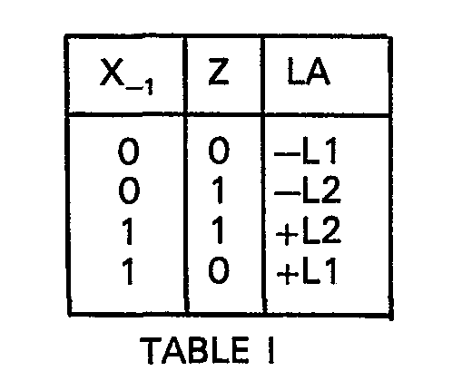
- the level LA of the signal present on wire 2 is determined as follows: the value of a logic variable Z is calculated by means of the expression and LA is given the level defined by the following table:
- Blocks D1, D2, D3, D4, E1, E2, G1, G2, composing block GSM are now examined in details.
- References E1, E2 denote two normal logic gates of exclusive ⁇ OR type; references D1 and D2 denote two normal delay cells, able to delay by one signalling period T the binary trains received at the input from wires 5 and 6 respectively; references D3 and D4 are delay cells analogous to D1 and D2, but able to delay the logic values received at their respective inputs by a time equal to half a signalling period (T/2), diminished by the response time ( ⁇ 1) introduced by gates E1, E2.
- References G1 and G2 denote two normal level generators each of them able to receive at the input two binary information signals and able also to emit at the output a signal level that can assume one among the four possible values iL1, +L2, according to the correspondence established in Tables I and II already examined.
- Binary signals X and Y corresponding to the already defined logic variables X o and Y -1/2 respectively, present on wires 5 and 6 respectively, are delayed by D1 and D2 by one signalling period T and emitted at the output on wires 7 and 8; therefore said signals present on wires 7 and 8 correspond to the previously examined logic variables X -1 and Y -3/2 respectively.
- Gate E1 receives at its two inputs, connected to wires 5 and 7 respectively both the signal of level X and the delayed repetition of the same, and emits at the output on wire 9 a binary signal that, with a lead equal to T/2, assumes the value of logic variable W already defined by the expression (2).
- Gate E2 has functions perfectly analogous to gate E1, but as regards the signal Y and its delayed repetition present on wires 6 and 8 respectively; E2 emits at the output on wire 10 a binary signal that, with a time lead equal to T/2 assumes the value of logic variable Z already defined by the expression (1).
- Delay cells D3 and D4 receive respectively from wires 9 and 10 the signals outgoing from gates E1 and E2 and emit at the output, respectively on wires 11 and 12, the same signals delayed by T/2; therefore said signals assume the values respectively of logic variables W and Z previously examined.
- Level generator G1 receives at the input, connected to wire 7, a binary signal having the value of the logic variable X_,, previously examined, and at the input connected to wire 12 a binary signal, having the value of logic variable Z, previously examined, and emits at the output on wire 2 a signal with level LA defined in Table I.
- Generator G2 has a perfectly analogous function as to what concerns binary signals Y -3/2 and W, received at the inputs connected to wires 8 and 11 respectively, and the signal outgoing on wire 3 of level LB, defined in Table II.
- the waveforms denoted by 2, 3, 5, 6, 7, 8, 9, 10, 11, 12 represent in a particular example of binary signals to be transmitted, just the signals present on the homonymous wires of Figure 2.
- Waveforms 5, 6, 7, 8, 9, 10, 11, 12 represent the values of logic variables under the assumption that the high level is associated to logic value 1 and the low level to logic value 0.
- Waveforms 2 and 3 represent levels LA and LB of modulating waveforms present on wires 2 and 3 respectively.
- the absolute value of levels ⁇ L2 is higher than the absolute value of levels ⁇ L1 and the ratio between said two absolute values is not given equal to any particular value. Yet generally the absolute value of levels +L2 can also be less than the absolute value of levels ⁇ L1.
- Reference ⁇ 1 denotes the delay time proper to gates E1 and E2. Such delay time is compensated for, in the example of Figure 3, by a reduced delay introduced by cells D3 and D4 of magnitude exactly equal to ⁇ 1.
- Reference ⁇ 2 denotes the proper delay time of level generators G1 and G2 that do not require any compensation.
- Waveforms 2 and 3 of Figure 3 outline that in correspondence with the sign changes of each one of the two waveforms, the absolute value of the other one is incremented by magnitude L2-L1.
- This increment of the absolute value of the amplitude of the modulating waveforms corresponds, after the amplitude modulation process operated by MP and MQ, to an incremented amplitude of the respective components of the quaternary phase-modulated signal, according to the principle disclosed with reference to Figure 1.
- the diagram of Figure 4 depicts, more particularly, a type of application in which the two components of the quaternary carrier are modulated first in sign and then in amplitude.
- references CG', PS', SS', D1', D2', D3', D4', E1', E2', AD' denote blocks perfectly identical to the homonymous blocks denoted, with only the apex excepted, in Figure 2.
- References M and M2 ( Figure 4) denote two normal modulators of the sign inversion type able to receive at the input, respectively from wires 13 and 14, periodical waveforms in order to operate the sign inversion on the basis of suitable control signals received from wires 15 and 16 respectively, and to emit said waveforms, possibly inverted, on the respective outputs connected to wires 17 and 18.
- References AT1, AT2 denote two normal attenuators apt to receive, from wires 17 and 18 respectively, modulated waveforms and to emit them on the respective outputs, connected to adder AD', at one of the two pre-determined amplitude levels LL1, LL2, in dependence on suitable control signals that AT1 and AT2 receive from wires 19 and 20 respectively.
- Blocks SS', D1', D2', D3', D4', E1', E2' are connected to one another exactly as their homonymous blocks denoted, with only the apex excepted, in Figure 2, and obviously carry out the same functions.
- level LA of the signal that modulates the phase-lead component is negative; whereas when X -1 assumes value 1, level LA is positive.
- the signals present on wires 19 and 20 represent a level that the components of the quaternary modulated signal can assume between the two possible levels: LL1, LL2; LL1 being for instance associated to the presence of a signal corresponding to logic value 1 and LL2 to the presence of a signal corresponding to logic value 0. That is the same as saying that, owing to the operation of blocks D2' and E2', for the phase-lead component the amplitude level LL1 is associated to the occurrence of a variation of the logic value of Y during the passage from one symbol to the next and the amplitude level LL2 is associated to the permanence of the logic value of Y during the passage from one symbol to the next.
- the amplitude level LL1 is associated to the occurrence of a variation of the logic value of X during the passage from one symbol to the next and the amplitude level LL2 is associated to the permanence of the logic value of X during the passage from one symbol to the next.
- the levels connected to the amplitude modulation can be of whatever number in function of the desired precision in correcting the spurious amplitude modulation, that occurs in relationship with the characteristics of the communication channel.
Landscapes
- Engineering & Computer Science (AREA)
- Computer Networks & Wireless Communication (AREA)
- Signal Processing (AREA)
- Digital Transmission Methods That Use Modulated Carrier Waves (AREA)
Description
- The invention relates to a quaternary modulation method of digital kind (PSK) in which the signal to be transmitted is divided into a first and a second binary signal train, phase-shifted relative to each other in time by half a symbol period; in which a first component of the carrier can assume and maintain during one symbol period one of two opposite phase states, said first component being phase-modulated in dependence on the symbols of said first binary train; in which a second carrier component can also assume and maintain during one symbol period one of two opposite phase states, said phase states being always in quadrature to those of the first component, said second component being phase-modulated in dependence on the symbols of said second binary train, said first and second carrier components being added together to obtain the quaternary signal, and to a device for realizing the method.
- It is well known that a carrier wave modulated in a PSK system is subject to a considerable amplitude modulation as a consequence of the necessary filtering operations that said modulated carrier wave must undergo. Because of this modulation the signal alters in an undesirable manner when it is transmitted over non-linear channels.
- In order to limit the extent of this modulation, various solutions have been suggested. These solutions can each be categorized as falling into one of the following four groups:
-
- a) modulation systems, so arranged as to obviate the phase transitions that would cause the greatest maxima of the amplitude modulation (S. A. Rhodes: "Effects of Hard Limiting on Band Limited Transmissions with Conventional and Offset QPSK Modulation", Proc. Nat., Telecom. Conf. (1972), pp. 20F1-20F7; R. K. Kwan: "The effect of filtering and limiting a double-binary PSK signal". IEEE Trans. On Aerospace and Electronic Systems, Vol. AES-5, n. 4, July 1969);
- b) systems in which, by means of storage circuits and function generators, an appropriate waveform is associated with each phase transition to be performed (M. K. Simon: "A generalization of Minimum-Shift-Keying (MSK)-type signaling based upon input data symbol pulse shaping", IEEE Trans. Communications, Vol. COM-24, pp. 845-856, August 1976; F. de Jager and C. B. Dekker: "Tamed Frequency Modulation, a novel method to achieve spectrum economy in digital transmission", IEEE Trans. Communications, Vol. COM-26, pp. 534-542, May 1978);
- c) systems in which the PSK signal is filtered by means of circuits performing non-linear operations so as to limit the amplitude modulation depth (C. J. Wolejsza: "State of the art of PSK modulation techniques", Colloque Int. sur les Telec. Numeriques par Satellite, Paris 1972);
- d) systems in which the amplitude modulation is duly reduced by means of a suitable choice of the time instants at which the carrier-phase transitions are forced (US-A-3914695).
- Systems of group a) provide an amplitude modulation which, though reduced, is still very high for transmission over non-linear channels.
- Systems of groups b) and c) make it possible to reduce amplitude modulation depth within reasonable limits; however they use complex and expensive circuits, difficult to reproduce and to adjust.
- The advantages offered by systems of group d) depend on the ratio of the band of the filters used to limit the signal bandwidth occupation, to the frequency at which the modulation is effected; therefore the field of application of the aforementioned systems is very limited.
- The invention is to solve the problem of providing for a low spurious amplitude modulation, by simple means in a manner easy to reproduce and with characteristics independent of the carrier frequency.
- Starting out from modulation systems catagorized in group a) and known from the literature relating to group a), this problem is solved by the invention which is characterized in that said first component is amplitude-modu-. lated in dependence on the sequence of symbols of said second binary train, and said second component is amplitude-modulated in dependence on the sequence of the symbols of said first binary train.
- The present invention applies to a Quaternary Phase Shift Keying system that corresponds to the sum of two bi-phase carriers duly phase-shifted and is adapted to the transmission of digital data previously subdivided into two binary signal trains, and also relates to a device in which the spurious amplitude modulation is compensated for, at least in part, by altering the amplitude of that component of the quaternary phase carrier which does not change its state in correspondence with the phase transitions of the modulated signal. The characteristics of said alterations, more particularly their amplitude, can be chosen so as to match the characteristics of the modulated signal to the characteristics of the communication channel over which it is sent, and thus can be tailored to the communication channel in order to optimize performance and trade off between quality and interferences. Moreover, the information signal can be recovered by the same demodulation and decision circuits which are usually adopted in the case of the conventional Quaternary Phase Shift Keying system.
- Amplitude modulating a PSK signal in dependence of its sequence of symbols is known per se (FR-A-2 173 642, DE-C-2 153 376), wherein some intersymbol-interference components resulting from the communication channel are compensated by a pre-distortion of the original binary signal which pre-distortion results in sending on the line a four-levels signal in place of the original two- levels signal. Even two components in phase quadrature may be each modulated by a sequence of binary symbols. Such technique, however, can not help to limit the amplitude modulation taking place in consequence of the necessary filter operations. Thus, it does not invite the person skilled in the art to derive therefrom the solution of the invention.
- These and other characteristics of the present invention will become clearer from the following description of two preferred ways of embodiment thereof, given by way of example and not in a limiting sense, with reference to the accompanying drawings, in which:
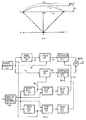
- Figure 1 is a vector diagram of a quaternary PSK signal, obtained by adding two biphase- signals in quadrature;
- Figure 2 is a block diagram of a first particular embodiment of the modulation method, object of the present invention, based on the amplitude alteration of the modulating waveforms;
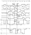
- Figure 3 is an example of waveforms of signals related to the diagram of Figure 2;
- Figure 4 is a block diagram of a second particular embodiment of the modulation method, object of the present invention, based on the amplitude alteration of the components forming the modulated carrier.
- Figure 1 schematically represents the principle on which the invention relies.
- Here, the quaternary modulated PSK signal, is represented by vector
OC , which is obtained by vectorially adding two components in quadrature to each other, represented by vectorsOA andOB . The two components are modulated by two different independent binary signal trains, each of them being associated with a step waveform. - The signalling intervals of the two binary signal trains, which modulate the two components of the quaternary carrier, are phase-shifted one with respect to the other by a time period equal to half the symbol period.
- This phase shift prevents the two components from changing their states simultaneously so that the resulting carrier can only have phase transitions of ±90°.
- Let assume, for instance, a phase transition of +90° of the carrier represented by vector
OC which, owing to the sign inversion of the component Oil from A to A', rotates from location OC to location OC'. - In case the principle of this invention was not applied, the trajectory along which the end of vector OC can move, in the transition from C to C', would only depend on the characteristics of the portion of transmission channel that is located prior to the observation point to which the vectorial diagram of Figure 1 is referred and on the phase of the carrier in correspondence with which the phase jump itself has been forced.
- Therefore it is impossible to predict what trajectory will be described by end C of vector OC.
- By way of example it can be supposed that, in case the principle of this invention was not applied, said transition might take place along the segment of straight line CC' including point B, that is, it might cover trajectory b.
- The principle on which the present invention relies consists in duly incrementing or decrementing, in correspondence with the phase transition of the carrier, the amplitude of the component which does not change its state; on the contrary when neither component changes its state, and therefore no phase transition occurs, no amplitude alteration takes place.
- In the case of phase transition +90°, shown in Figure 1, said principle is realized by altering, in the particular case of positive increment, the amplitude of the component
OB which does not change its state. - Due to said alteration, the trajectory covered by end C of vector
OG is, for instance, trajectory c instead of b. - The shape of trajectory c depends on the actual shape of the trajectory in case the principle upon which this invention relies was not applied (in the example of Figure 1, trajectory b) and obviously on the degree of alteration produced on the component that does not change its state; the degree of said alteration is determined so as to optimize the communication channel performance.
- In a solution of the adaptive kind, it will be sufficient to simulate the communication channel response and utilize in real time the results in order to choose the degree of said alteration; but in the most general cases said alteration can be determined once for all while planning the design.
- Hereinafter, to simplify the description, only the case will be considered in which the degree of said alteration is predetermined and kept equal for all phase transitions of the carrier.
- In the example depicted in Figure 1 the alteration of the amplitude of component 09 has been assumed to be such as to reduce the spurious amplitude modulation associated with phase transition, by making end C follow trajectory c.
- In fact, if phase transition were to occur without the modulated signal being affected by spurious amplitude modulation, end C of the vector representing said signal would cover an arc of circumference (dashed curve a) in its transition from C to C'.
- The changes of amplitude connected to other trajectories can be measured with respect to said circumference arc along the half-lines outgoing from 0.
- As shown in the drawing, the maximum (m,) amplitude shift of trajectory b with respect to trajectory a is greater than the maximum (m2) amplitude shift of trajectory c with respect to circular trajectory a.
- It is now worth noting that the improvement in the performance relating to the communication channel, generally, is not connected to the decreasing of the maximum of spurious amplitude modulation.
- For instance, if in the channel non-linear elements were present the application of the present principle could be oriented to obtain minimum degradation due to non-linearity effects.
- In some particular cases, the inventor has even found it convenient to predetermine a reduction in the amplitude of the component that does not change its state, in correspondence with phase transitions in quaternary carrier.
- Figure 2 is referred to a particular example of application of the present invention, in which the amplitude of base-band modulating signals is modified, i.e. the amplitude of the two signals modulating the two biphase carriers composing the quaternary signal.
- In Figure 2 reference GSM denotes the particular circuit that realizes the present invention; said circuit is able to receive at the input two binary signal trains having the signalling interval phase-shifted relative to each other by half signalling period T, and able also to emit at the output two waveforms, each one having four levels, utilized to amplitude-modulate the two components in quadrature of the quaternary signal.
- The blocks forming GSM as well as their functions will be described in details hereinafter.
- SS denotes a normal encoding circuit able to serially receive, at the input connected to wire '1, the binary digits of the information to the transmitted and convert them into two binary signal trains having the signalling period T equal to twice the signalling period of the input sequence; said trains, which are phase-shifted with respect to each other by half their signalling period T, are separately emitted at the output over
wires - Reference CG denotes a usual generator of carrier wave; reference PS denotes a usual circuit able to introduce a phase delay of 90° between the signal emitted at the output and the one received at the input; references MQ and MP denote two usual amplitude modulators; reference AD denotes a normal adder circuit.
- The network composed of blocks CG, PS, MQ, MP and AD is a structure well known in the technique as being able to generate and modulate a quaternary carrier.
- More particularly, said structure receives from
wires wire 4. - In order to allow better understanding of the structure and operation of block GSM, the description of the operating theoretical principle is now anticipated.
- Let references ±L1, and ±L2 denote the levels utilized to define levels LA and LB of the modulating signals present on
wires wires wire 2; let references X0, X-1 denote the logic levels present onwire 5 respectively at the time instants t=0 and t=-T and analogously let references Y-1/2, Y-3/2 denote the logic levels present onwire 6, respectively at time intervals t=-T/2 and t=-3/2T. - The level LA of the signal present on
wire 2 is determined as follows: the value of a logic variable Z is calculated by means of the expression
- Level LB, that is maintained during the signalling interval beginning at instant t=0, is determined as follows: the value of a logic variable W is computed by means of the expression:


- Blocks D1, D2, D3, D4, E1, E2, G1, G2, composing block GSM are now examined in details.
- References E1, E2 denote two normal logic gates of exclusive ―OR type; references D1 and D2 denote two normal delay cells, able to delay by one signalling period T the binary trains received at the input from
wires - References G1 and G2 denote two normal level generators each of them able to receive at the input two binary information signals and able also to emit at the output a signal level that can assume one among the four possible values iL1, +L2, according to the correspondence established in Tables I and II already examined.
- The operation of block GSM will now be investigated.
- Binary signals X and Y corresponding to the already defined logic variables Xo and Y-1/2 respectively, present on
wires wires wires - Gate E1 receives at its two inputs, connected to
wires - Gate E2 has functions perfectly analogous to gate E1, but as regards the signal Y and its delayed repetition present on
wires - Delay cells D3 and D4 receive respectively from
wires wires - Level generator G1 receives at the input, connected to
wire 7, a binary signal having the value of the logic variable X_,, previously examined, and at the input connected to wire 12 a binary signal, having the value of logic variable Z, previously examined, and emits at the output on wire 2 a signal with level LA defined in Table I. - Generator G2 has a perfectly analogous function as to what concerns binary signals Y-3/2 and W, received at the inputs connected to
wires wire 3 of level LB, defined in Table II. - In Figure 3, the waveforms denoted by 2, 3, 5, 6, 7, 8, 9, 10, 11, 12 represent in a particular example of binary signals to be transmitted, just the signals present on the homonymous wires of Figure 2.
- The time scale t is normalized with respect to signalling period T and the origin t=0 has been arbitrarily chosen by way of example in correspondence with the central instant of a signalling interval of modulating
waveform 2. -
Waveforms logic value 1 and the low level tologic value 0. -
Waveforms wires - In the particular example of Figure 3 the absolute value of levels ±L2 is higher than the absolute value of levels ±L1 and the ratio between said two absolute values is not given equal to any particular value. Yet generally the absolute value of levels +L2 can also be less than the absolute value of levels ±L1.
- Reference △1 denotes the delay time proper to gates E1 and E2. Such delay time is compensated for, in the example of Figure 3, by a reduced delay introduced by cells D3 and D4 of magnitude exactly equal to △1.
- Reference Δ2 denotes the proper delay time of level generators G1 and G2 that do not require any compensation.
-
Waveforms - This increment of the absolute value of the amplitude of the modulating waveforms corresponds, after the amplitude modulation process operated by MP and MQ, to an incremented amplitude of the respective components of the quaternary phase-modulated signal, according to the principle disclosed with reference to Figure 1.
- In this way by MP and MQ a four-level (±L1; ±L2) modulation is carried out that gives rise in the two modulated components to two different amplitude levels in addition to a possible sign inversion, that is a two-level amplitude modulation in addition to a two-stages phase modulation.
- The same result can be obtained by modulating the two components of the quaternary carrier first in sign and then in amplitude or vice-versa.
- The diagram of Figure 4 depicts, more particularly, a type of application in which the two components of the quaternary carrier are modulated first in sign and then in amplitude.
- In Figure 4 references CG', PS', SS', D1', D2', D3', D4', E1', E2', AD' denote blocks perfectly identical to the homonymous blocks denoted, with only the apex excepted, in Figure 2.
- References M and M2 (Figure 4) denote two normal modulators of the sign inversion type able to receive at the input, respectively from
wires wires wires - References AT1, AT2 denote two normal attenuators apt to receive, from
wires wires - Blocks SS', D1', D2', D3', D4', E1', E2', are connected to one another exactly as their homonymous blocks denoted, with only the apex excepted, in Figure 2, and obviously carry out the same functions.
- Therefore the signals present on
wires wires 19 and 20 (Figure 4) correspond to the logic variables W (Table II) and Z (Table I), respectively. - The principle on which the particular diagram of Figure 4 relies depends on the consideration that the logic variables X-1 and Y-3/2 are in relationship, as clearly results from Tables I and II, respectively with the sign of the component directly coming from CG', having a phase lead of 45° with respect to non-modulated carrier, and with the sign of the component coming from PS', having a phase-lag of 45° with respect to non-modulated carrier.
- In fact, when X-1 (Table I) assumes
logic value 0, level LA of the signal that modulates the phase-lead component is negative; whereas when X-1 assumesvalue 1, level LA is positive. - Analogously, when Y-3/2 (Table II) assumes
logic value 0, level LB of the signal modulating the phase-lag component is negative; whereas when Y-3/2 assumeslogic value 1, level LB is positive. - From these considerations it results that the signals present on
wires - Analogously the signals present on
wires logic value 1 and LL2 to the presence of a signal corresponding tologic value 0. That is the same as saying that, owing to the operation of blocks D2' and E2', for the phase-lead component the amplitude level LL1 is associated to the occurrence of a variation of the logic value of Y during the passage from one symbol to the next and the amplitude level LL2 is associated to the permanence of the logic value of Y during the passage from one symbol to the next. - Analogously, for the phase-lag component the amplitude level LL1 is associated to the occurrence of a variation of the logic value of X during the passage from one symbol to the next and the amplitude level LL2 is associated to the permanence of the logic value of X during the passage from one symbol to the next.
- This interpretation of the amplitude level association of the two components to the variations and permanences of the logic values of variables X and Y can obviously be also referred to the particular example of embodiment depicted in Figure 2, according to what mentioned in reference to Figure 3.
- It is now to be specified that the levels connected to the amplitude modulation (assumed thus far for simplicity in number of two: LL1, LL2) can be of whatever number in function of the desired precision in correcting the spurious amplitude modulation, that occurs in relationship with the characteristics of the communication channel.
- The extension entailing multilevel amplitude modulation is not anyway a problem to the skilled in the art.
- In our example, it will be enough to replace blocks D1, E1, D3 (Figure 2) and blocks D2, E2, E4 by two digital filters of any known type, able to generate at the output multilevel signals depending on the digital signals received at the input.
- Analogously in the scheme of Figure 4 it will be sufficient to replace blocks D1', E1', D3' and blocks D2', E2', D4' by filters of the same kind.
Claims (7)
Applications Claiming Priority (2)
| Application Number | Priority Date | Filing Date | Title |
|---|---|---|---|
| IT6947178 | 1978-10-27 | ||
| IT69471/78A IT1160910B (en) | 1978-10-27 | 1978-10-27 | FOUR-PHASE MODULATION SYSTEM FOR TRANSMISSION OF NUMERICAL INFORMATION |
Publications (2)
| Publication Number | Publication Date |
|---|---|
| EP0010731A1 EP0010731A1 (en) | 1980-05-14 |
| EP0010731B1 true EP0010731B1 (en) | 1983-06-22 |
Family
ID=11312206
Family Applications (1)
| Application Number | Title | Priority Date | Filing Date |
|---|---|---|---|
| EP79104126A Expired EP0010731B1 (en) | 1978-10-27 | 1979-10-25 | Quaternary modulation method for digital data transmission and device for realizing this method |
Country Status (3)
| Country | Link |
|---|---|
| EP (1) | EP0010731B1 (en) |
| DE (1) | DE2965751D1 (en) |
| IT (1) | IT1160910B (en) |
Families Citing this family (3)
| Publication number | Priority date | Publication date | Assignee | Title |
|---|---|---|---|---|
| EP0197529B1 (en) * | 1985-04-23 | 1992-02-05 | Josef Dirr | Method for the analogous or digital coding of information for use in angle and pulse modulation processes |
| US6101225A (en) * | 1998-04-29 | 2000-08-08 | Motorola, Inc. | Method and apparatus for performing a modulation |
| US11792777B2 (en) * | 2020-08-03 | 2023-10-17 | Qualcomm Incorporated | Peak to average power ratio reduction for supplementary uplink |
Family Cites Families (3)
| Publication number | Priority date | Publication date | Assignee | Title |
|---|---|---|---|---|
| US3406343A (en) * | 1965-07-01 | 1968-10-15 | Rca Corp | Pm/am multiplex communication |
| DE2153376B2 (en) * | 1971-10-27 | 1976-09-30 | Fujitsu Ltd., Kawasaki, Kanagawa (Japan) | DIGITAL MESSAGE TRANSFER ARRANGEMENT |
| IT991725B (en) * | 1973-07-12 | 1975-08-30 | Cselt Centro Studi Lab Telecom | FOUR-PHASE MODULATION SYSTEM FOR THE TRANSMISSION OF NUMERICAL INFORMATION |
-
1978
- 1978-10-27 IT IT69471/78A patent/IT1160910B/en active
-
1979
- 1979-10-25 EP EP79104126A patent/EP0010731B1/en not_active Expired
- 1979-10-25 DE DE7979104126T patent/DE2965751D1/en not_active Expired
Also Published As
| Publication number | Publication date |
|---|---|
| EP0010731A1 (en) | 1980-05-14 |
| DE2965751D1 (en) | 1983-07-28 |
| IT1160910B (en) | 1987-03-11 |
| IT7869471A0 (en) | 1978-10-27 |
Similar Documents
| Publication | Publication Date | Title |
|---|---|---|
| Linz et al. | Efficient implementation of an IQ GMSK modulator | |
| US5285479A (en) | Quadrature modulation circuit | |
| US4613976A (en) | Constant envelope offset QPSK modulator | |
| US4338579A (en) | Frequency shift offset quadrature modulation and demodulation | |
| KR100311072B1 (en) | Baseband Signal Generator for Multiple-value Nested Amplitude Modulation | |
| US3760277A (en) | Coding and decoding system with multi-level format | |
| EP0440187A2 (en) | Arrangement for converting binary input signal into corresponding in-phase and quadrature phase signals | |
| DE2153376B2 (en) | DIGITAL MESSAGE TRANSFER ARRANGEMENT | |
| EP0531100B1 (en) | Baseband pulse shaper for GMSK modulators | |
| US5027372A (en) | Differential phase shift keying modulator | |
| DE10318643B4 (en) | Multi-valued FSK frequency modulation system | |
| AU619398B2 (en) | Wave form generator | |
| EP0010731A1 (en) | Quaternary modulation method for digital data transmission and device for realizing this method | |
| US4500856A (en) | Simplified minimum shift keying modulator | |
| US3659207A (en) | Multi-waveform generation from a single tapped delay line | |
| US4210879A (en) | Four-phase staggered shift keying modulator system | |
| US3213369A (en) | Data control of carrier injection in sideband transmission systems | |
| US6430232B1 (en) | Phase constellation modulator | |
| Aein et al. | Effect of co-channel interference on CPSK carriers | |
| GB2038143A (en) | Circuit arrangements for converting binary digital signals to pseudo-ternary alternating pulses | |
| CA1226067A (en) | Multi-function data signal processing method and apparatus | |
| GB1318531A (en) | Data signal transmission system employing phase modulation | |
| Ruthroff et al. | Adaptive coding for coherent detection of digital phase modulation | |
| US3992673A (en) | System for demodulating a digital modulated wave | |
| EP0220705A2 (en) | Quadriphase phase modulation system |
Legal Events
| Date | Code | Title | Description |
|---|---|---|---|
| PUAI | Public reference made under article 153(3) epc to a published international application that has entered the european phase |
Free format text: ORIGINAL CODE: 0009012 |
|
| AK | Designated contracting states |
Designated state(s): DE FR GB |
|
| 17P | Request for examination filed | ||
| DET | De: translation of patent claims | ||
| GRAA | (expected) grant |
Free format text: ORIGINAL CODE: 0009210 |
|
| AK | Designated contracting states |
Designated state(s): DE FR GB |
|
| REF | Corresponds to: |
Ref document number: 2965751 Country of ref document: DE Date of ref document: 19830728 |
|
| ET | Fr: translation filed | ||
| PLBE | No opposition filed within time limit |
Free format text: ORIGINAL CODE: 0009261 |
|
| STAA | Information on the status of an ep patent application or granted ep patent |
Free format text: STATUS: NO OPPOSITION FILED WITHIN TIME LIMIT |
|
| 26N | No opposition filed | ||
| PGFP | Annual fee paid to national office [announced via postgrant information from national office to epo] |
Ref country code: DE Payment date: 19841029 Year of fee payment: 6 |
|
| PGFP | Annual fee paid to national office [announced via postgrant information from national office to epo] |
Ref country code: FR Payment date: 19841031 Year of fee payment: 6 |
|
| GBPC | Gb: european patent ceased through non-payment of renewal fee | ||
| PG25 | Lapsed in a contracting state [announced via postgrant information from national office to epo] |
Ref country code: FR Free format text: LAPSE BECAUSE OF NON-PAYMENT OF DUE FEES Effective date: 19880630 |
|
| PG25 | Lapsed in a contracting state [announced via postgrant information from national office to epo] |
Ref country code: DE Effective date: 19880701 |
|
| REG | Reference to a national code |
Ref country code: FR Ref legal event code: ST |
|
| PG25 | Lapsed in a contracting state [announced via postgrant information from national office to epo] |
Ref country code: GB Effective date: 19881118 |