EP0009131A1 - Process for in situ modification of solder alloy compositions - Google Patents
Process for in situ modification of solder alloy compositions Download PDFInfo
- Publication number
- EP0009131A1 EP0009131A1 EP79103107A EP79103107A EP0009131A1 EP 0009131 A1 EP0009131 A1 EP 0009131A1 EP 79103107 A EP79103107 A EP 79103107A EP 79103107 A EP79103107 A EP 79103107A EP 0009131 A1 EP0009131 A1 EP 0009131A1
- Authority
- EP
- European Patent Office
- Prior art keywords
- solder
- indium
- flux
- lead
- alloy
- Prior art date
- Legal status (The legal status is an assumption and is not a legal conclusion. Google has not performed a legal analysis and makes no representation as to the accuracy of the status listed.)
- Granted
Links
Images


Classifications
-
- H—ELECTRICITY
- H01—ELECTRIC ELEMENTS
- H01L—SEMICONDUCTOR DEVICES NOT COVERED BY CLASS H10
- H01L24/00—Arrangements for connecting or disconnecting semiconductor or solid-state bodies; Methods or apparatus related thereto
- H01L24/01—Means for bonding being attached to, or being formed on, the surface to be connected, e.g. chip-to-package, die-attach, "first-level" interconnects; Manufacturing methods related thereto
- H01L24/10—Bump connectors ; Manufacturing methods related thereto
-
- B—PERFORMING OPERATIONS; TRANSPORTING
- B23—MACHINE TOOLS; METAL-WORKING NOT OTHERWISE PROVIDED FOR
- B23K—SOLDERING OR UNSOLDERING; WELDING; CLADDING OR PLATING BY SOLDERING OR WELDING; CUTTING BY APPLYING HEAT LOCALLY, e.g. FLAME CUTTING; WORKING BY LASER BEAM
- B23K35/00—Rods, electrodes, materials, or media, for use in soldering, welding, or cutting
- B23K35/22—Rods, electrodes, materials, or media, for use in soldering, welding, or cutting characterised by the composition or nature of the material
- B23K35/24—Selection of soldering or welding materials proper
- B23K35/26—Selection of soldering or welding materials proper with the principal constituent melting at less than 400 degrees C
- B23K35/268—Pb as the principal constituent
-
- B—PERFORMING OPERATIONS; TRANSPORTING
- B23—MACHINE TOOLS; METAL-WORKING NOT OTHERWISE PROVIDED FOR
- B23K—SOLDERING OR UNSOLDERING; WELDING; CLADDING OR PLATING BY SOLDERING OR WELDING; CUTTING BY APPLYING HEAT LOCALLY, e.g. FLAME CUTTING; WORKING BY LASER BEAM
- B23K35/00—Rods, electrodes, materials, or media, for use in soldering, welding, or cutting
- B23K35/22—Rods, electrodes, materials, or media, for use in soldering, welding, or cutting characterised by the composition or nature of the material
- B23K35/36—Selection of non-metallic compositions, e.g. coatings, fluxes; Selection of soldering or welding materials, conjoint with selection of non-metallic compositions, both selections being of interest
- B23K35/3612—Selection of non-metallic compositions, e.g. coatings, fluxes; Selection of soldering or welding materials, conjoint with selection of non-metallic compositions, both selections being of interest with organic compounds as principal constituents
- B23K35/3618—Carboxylic acids or salts
-
- H—ELECTRICITY
- H01—ELECTRIC ELEMENTS
- H01L—SEMICONDUCTOR DEVICES NOT COVERED BY CLASS H10
- H01L23/00—Details of semiconductor or other solid state devices
- H01L23/48—Arrangements for conducting electric current to or from the solid state body in operation, e.g. leads, terminal arrangements ; Selection of materials therefor
- H01L23/488—Arrangements for conducting electric current to or from the solid state body in operation, e.g. leads, terminal arrangements ; Selection of materials therefor consisting of soldered or bonded constructions
-
- H—ELECTRICITY
- H01—ELECTRIC ELEMENTS
- H01L—SEMICONDUCTOR DEVICES NOT COVERED BY CLASS H10
- H01L24/00—Arrangements for connecting or disconnecting semiconductor or solid-state bodies; Methods or apparatus related thereto
- H01L24/01—Means for bonding being attached to, or being formed on, the surface to be connected, e.g. chip-to-package, die-attach, "first-level" interconnects; Manufacturing methods related thereto
- H01L24/10—Bump connectors ; Manufacturing methods related thereto
- H01L24/12—Structure, shape, material or disposition of the bump connectors prior to the connecting process
- H01L24/13—Structure, shape, material or disposition of the bump connectors prior to the connecting process of an individual bump connector
-
- H—ELECTRICITY
- H01—ELECTRIC ELEMENTS
- H01L—SEMICONDUCTOR DEVICES NOT COVERED BY CLASS H10
- H01L2224/00—Indexing scheme for arrangements for connecting or disconnecting semiconductor or solid-state bodies and methods related thereto as covered by H01L24/00
- H01L2224/01—Means for bonding being attached to, or being formed on, the surface to be connected, e.g. chip-to-package, die-attach, "first-level" interconnects; Manufacturing methods related thereto
- H01L2224/02—Bonding areas; Manufacturing methods related thereto
- H01L2224/04—Structure, shape, material or disposition of the bonding areas prior to the connecting process
- H01L2224/05—Structure, shape, material or disposition of the bonding areas prior to the connecting process of an individual bonding area
- H01L2224/05001—Internal layers
- H01L2224/05099—Material
- H01L2224/051—Material with a principal constituent of the material being a metal or a metalloid, e.g. boron [B], silicon [Si], germanium [Ge], arsenic [As], antimony [Sb], tellurium [Te] and polonium [Po], and alloys thereof
- H01L2224/05117—Material with a principal constituent of the material being a metal or a metalloid, e.g. boron [B], silicon [Si], germanium [Ge], arsenic [As], antimony [Sb], tellurium [Te] and polonium [Po], and alloys thereof the principal constituent melting at a temperature of greater than or equal to 400°C and less than 950°C
- H01L2224/05124—Aluminium [Al] as principal constituent
-
- H—ELECTRICITY
- H01—ELECTRIC ELEMENTS
- H01L—SEMICONDUCTOR DEVICES NOT COVERED BY CLASS H10
- H01L2224/00—Indexing scheme for arrangements for connecting or disconnecting semiconductor or solid-state bodies and methods related thereto as covered by H01L24/00
- H01L2224/01—Means for bonding being attached to, or being formed on, the surface to be connected, e.g. chip-to-package, die-attach, "first-level" interconnects; Manufacturing methods related thereto
- H01L2224/02—Bonding areas; Manufacturing methods related thereto
- H01L2224/04—Structure, shape, material or disposition of the bonding areas prior to the connecting process
- H01L2224/05—Structure, shape, material or disposition of the bonding areas prior to the connecting process of an individual bonding area
- H01L2224/05001—Internal layers
- H01L2224/05099—Material
- H01L2224/051—Material with a principal constituent of the material being a metal or a metalloid, e.g. boron [B], silicon [Si], germanium [Ge], arsenic [As], antimony [Sb], tellurium [Te] and polonium [Po], and alloys thereof
- H01L2224/05138—Material with a principal constituent of the material being a metal or a metalloid, e.g. boron [B], silicon [Si], germanium [Ge], arsenic [As], antimony [Sb], tellurium [Te] and polonium [Po], and alloys thereof the principal constituent melting at a temperature of greater than or equal to 950°C and less than 1550°C
- H01L2224/05147—Copper [Cu] as principal constituent
-
- H—ELECTRICITY
- H01—ELECTRIC ELEMENTS
- H01L—SEMICONDUCTOR DEVICES NOT COVERED BY CLASS H10
- H01L2224/00—Indexing scheme for arrangements for connecting or disconnecting semiconductor or solid-state bodies and methods related thereto as covered by H01L24/00
- H01L2224/01—Means for bonding being attached to, or being formed on, the surface to be connected, e.g. chip-to-package, die-attach, "first-level" interconnects; Manufacturing methods related thereto
- H01L2224/02—Bonding areas; Manufacturing methods related thereto
- H01L2224/04—Structure, shape, material or disposition of the bonding areas prior to the connecting process
- H01L2224/05—Structure, shape, material or disposition of the bonding areas prior to the connecting process of an individual bonding area
- H01L2224/05001—Internal layers
- H01L2224/05099—Material
- H01L2224/051—Material with a principal constituent of the material being a metal or a metalloid, e.g. boron [B], silicon [Si], germanium [Ge], arsenic [As], antimony [Sb], tellurium [Te] and polonium [Po], and alloys thereof
- H01L2224/05163—Material with a principal constituent of the material being a metal or a metalloid, e.g. boron [B], silicon [Si], germanium [Ge], arsenic [As], antimony [Sb], tellurium [Te] and polonium [Po], and alloys thereof the principal constituent melting at a temperature of greater than 1550°C
- H01L2224/05171—Chromium [Cr] as principal constituent
-
- H—ELECTRICITY
- H01—ELECTRIC ELEMENTS
- H01L—SEMICONDUCTOR DEVICES NOT COVERED BY CLASS H10
- H01L2224/00—Indexing scheme for arrangements for connecting or disconnecting semiconductor or solid-state bodies and methods related thereto as covered by H01L24/00
- H01L2224/01—Means for bonding being attached to, or being formed on, the surface to be connected, e.g. chip-to-package, die-attach, "first-level" interconnects; Manufacturing methods related thereto
- H01L2224/02—Bonding areas; Manufacturing methods related thereto
- H01L2224/04—Structure, shape, material or disposition of the bonding areas prior to the connecting process
- H01L2224/05—Structure, shape, material or disposition of the bonding areas prior to the connecting process of an individual bonding area
- H01L2224/0554—External layer
- H01L2224/05599—Material
- H01L2224/056—Material with a principal constituent of the material being a metal or a metalloid, e.g. boron [B], silicon [Si], germanium [Ge], arsenic [As], antimony [Sb], tellurium [Te] and polonium [Po], and alloys thereof
- H01L2224/05638—Material with a principal constituent of the material being a metal or a metalloid, e.g. boron [B], silicon [Si], germanium [Ge], arsenic [As], antimony [Sb], tellurium [Te] and polonium [Po], and alloys thereof the principal constituent melting at a temperature of greater than or equal to 950°C and less than 1550°C
- H01L2224/05644—Gold [Au] as principal constituent
-
- H—ELECTRICITY
- H01—ELECTRIC ELEMENTS
- H01L—SEMICONDUCTOR DEVICES NOT COVERED BY CLASS H10
- H01L2224/00—Indexing scheme for arrangements for connecting or disconnecting semiconductor or solid-state bodies and methods related thereto as covered by H01L24/00
- H01L2224/01—Means for bonding being attached to, or being formed on, the surface to be connected, e.g. chip-to-package, die-attach, "first-level" interconnects; Manufacturing methods related thereto
- H01L2224/10—Bump connectors; Manufacturing methods related thereto
- H01L2224/12—Structure, shape, material or disposition of the bump connectors prior to the connecting process
- H01L2224/13—Structure, shape, material or disposition of the bump connectors prior to the connecting process of an individual bump connector
- H01L2224/13001—Core members of the bump connector
- H01L2224/13099—Material
-
- H—ELECTRICITY
- H01—ELECTRIC ELEMENTS
- H01L—SEMICONDUCTOR DEVICES NOT COVERED BY CLASS H10
- H01L2224/00—Indexing scheme for arrangements for connecting or disconnecting semiconductor or solid-state bodies and methods related thereto as covered by H01L24/00
- H01L2224/01—Means for bonding being attached to, or being formed on, the surface to be connected, e.g. chip-to-package, die-attach, "first-level" interconnects; Manufacturing methods related thereto
- H01L2224/10—Bump connectors; Manufacturing methods related thereto
- H01L2224/12—Structure, shape, material or disposition of the bump connectors prior to the connecting process
- H01L2224/13—Structure, shape, material or disposition of the bump connectors prior to the connecting process of an individual bump connector
- H01L2224/1354—Coating
- H01L2224/13599—Material
- H01L2224/136—Material with a principal constituent of the material being a metal or a metalloid, e.g. boron [B], silicon [Si], germanium [Ge], arsenic [As], antimony [Sb], tellurium [Te] and polonium [Po], and alloys thereof
- H01L2224/13601—Material with a principal constituent of the material being a metal or a metalloid, e.g. boron [B], silicon [Si], germanium [Ge], arsenic [As], antimony [Sb], tellurium [Te] and polonium [Po], and alloys thereof the principal constituent melting at a temperature of less than 400°C
- H01L2224/13609—Indium [In] as principal constituent
-
- H—ELECTRICITY
- H01—ELECTRIC ELEMENTS
- H01L—SEMICONDUCTOR DEVICES NOT COVERED BY CLASS H10
- H01L2224/00—Indexing scheme for arrangements for connecting or disconnecting semiconductor or solid-state bodies and methods related thereto as covered by H01L24/00
- H01L2224/01—Means for bonding being attached to, or being formed on, the surface to be connected, e.g. chip-to-package, die-attach, "first-level" interconnects; Manufacturing methods related thereto
- H01L2224/10—Bump connectors; Manufacturing methods related thereto
- H01L2224/15—Structure, shape, material or disposition of the bump connectors after the connecting process
- H01L2224/16—Structure, shape, material or disposition of the bump connectors after the connecting process of an individual bump connector
-
- H—ELECTRICITY
- H01—ELECTRIC ELEMENTS
- H01L—SEMICONDUCTOR DEVICES NOT COVERED BY CLASS H10
- H01L2924/00—Indexing scheme for arrangements or methods for connecting or disconnecting semiconductor or solid-state bodies as covered by H01L24/00
- H01L2924/01—Chemical elements
- H01L2924/01012—Magnesium [Mg]
-
- H—ELECTRICITY
- H01—ELECTRIC ELEMENTS
- H01L—SEMICONDUCTOR DEVICES NOT COVERED BY CLASS H10
- H01L2924/00—Indexing scheme for arrangements or methods for connecting or disconnecting semiconductor or solid-state bodies as covered by H01L24/00
- H01L2924/01—Chemical elements
- H01L2924/01013—Aluminum [Al]
-
- H—ELECTRICITY
- H01—ELECTRIC ELEMENTS
- H01L—SEMICONDUCTOR DEVICES NOT COVERED BY CLASS H10
- H01L2924/00—Indexing scheme for arrangements or methods for connecting or disconnecting semiconductor or solid-state bodies as covered by H01L24/00
- H01L2924/01—Chemical elements
- H01L2924/01023—Vanadium [V]
-
- H—ELECTRICITY
- H01—ELECTRIC ELEMENTS
- H01L—SEMICONDUCTOR DEVICES NOT COVERED BY CLASS H10
- H01L2924/00—Indexing scheme for arrangements or methods for connecting or disconnecting semiconductor or solid-state bodies as covered by H01L24/00
- H01L2924/01—Chemical elements
- H01L2924/01024—Chromium [Cr]
-
- H—ELECTRICITY
- H01—ELECTRIC ELEMENTS
- H01L—SEMICONDUCTOR DEVICES NOT COVERED BY CLASS H10
- H01L2924/00—Indexing scheme for arrangements or methods for connecting or disconnecting semiconductor or solid-state bodies as covered by H01L24/00
- H01L2924/01—Chemical elements
- H01L2924/01029—Copper [Cu]
-
- H—ELECTRICITY
- H01—ELECTRIC ELEMENTS
- H01L—SEMICONDUCTOR DEVICES NOT COVERED BY CLASS H10
- H01L2924/00—Indexing scheme for arrangements or methods for connecting or disconnecting semiconductor or solid-state bodies as covered by H01L24/00
- H01L2924/01—Chemical elements
- H01L2924/01049—Indium [In]
-
- H—ELECTRICITY
- H01—ELECTRIC ELEMENTS
- H01L—SEMICONDUCTOR DEVICES NOT COVERED BY CLASS H10
- H01L2924/00—Indexing scheme for arrangements or methods for connecting or disconnecting semiconductor or solid-state bodies as covered by H01L24/00
- H01L2924/01—Chemical elements
- H01L2924/01057—Lanthanum [La]
-
- H—ELECTRICITY
- H01—ELECTRIC ELEMENTS
- H01L—SEMICONDUCTOR DEVICES NOT COVERED BY CLASS H10
- H01L2924/00—Indexing scheme for arrangements or methods for connecting or disconnecting semiconductor or solid-state bodies as covered by H01L24/00
- H01L2924/01—Chemical elements
- H01L2924/01079—Gold [Au]
-
- H—ELECTRICITY
- H01—ELECTRIC ELEMENTS
- H01L—SEMICONDUCTOR DEVICES NOT COVERED BY CLASS H10
- H01L2924/00—Indexing scheme for arrangements or methods for connecting or disconnecting semiconductor or solid-state bodies as covered by H01L24/00
- H01L2924/01—Chemical elements
- H01L2924/01082—Lead [Pb]
-
- H—ELECTRICITY
- H01—ELECTRIC ELEMENTS
- H01L—SEMICONDUCTOR DEVICES NOT COVERED BY CLASS H10
- H01L2924/00—Indexing scheme for arrangements or methods for connecting or disconnecting semiconductor or solid-state bodies as covered by H01L24/00
- H01L2924/013—Alloys
- H01L2924/014—Solder alloys
-
- H—ELECTRICITY
- H01—ELECTRIC ELEMENTS
- H01L—SEMICONDUCTOR DEVICES NOT COVERED BY CLASS H10
- H01L2924/00—Indexing scheme for arrangements or methods for connecting or disconnecting semiconductor or solid-state bodies as covered by H01L24/00
- H01L2924/10—Details of semiconductor or other solid state devices to be connected
- H01L2924/11—Device type
- H01L2924/14—Integrated circuits
-
- H—ELECTRICITY
- H01—ELECTRIC ELEMENTS
- H01L—SEMICONDUCTOR DEVICES NOT COVERED BY CLASS H10
- H01L2924/00—Indexing scheme for arrangements or methods for connecting or disconnecting semiconductor or solid-state bodies as covered by H01L24/00
- H01L2924/15—Details of package parts other than the semiconductor or other solid state devices to be connected
- H01L2924/151—Die mounting substrate
- H01L2924/156—Material
- H01L2924/15786—Material with a principal constituent of the material being a non metallic, non metalloid inorganic material
- H01L2924/15787—Ceramics, e.g. crystalline carbides, nitrides or oxides
-
- H—ELECTRICITY
- H05—ELECTRIC TECHNIQUES NOT OTHERWISE PROVIDED FOR
- H05K—PRINTED CIRCUITS; CASINGS OR CONSTRUCTIONAL DETAILS OF ELECTRIC APPARATUS; MANUFACTURE OF ASSEMBLAGES OF ELECTRICAL COMPONENTS
- H05K3/00—Apparatus or processes for manufacturing printed circuits
- H05K3/30—Assembling printed circuits with electric components, e.g. with resistor
- H05K3/32—Assembling printed circuits with electric components, e.g. with resistor electrically connecting electric components or wires to printed circuits
- H05K3/34—Assembling printed circuits with electric components, e.g. with resistor electrically connecting electric components or wires to printed circuits by soldering
- H05K3/3457—Solder materials or compositions; Methods of application thereof
- H05K3/3463—Solder compositions in relation to features of the printed circuit board or the mounting process
-
- H—ELECTRICITY
- H05—ELECTRIC TECHNIQUES NOT OTHERWISE PROVIDED FOR
- H05K—PRINTED CIRCUITS; CASINGS OR CONSTRUCTIONAL DETAILS OF ELECTRIC APPARATUS; MANUFACTURE OF ASSEMBLAGES OF ELECTRICAL COMPONENTS
- H05K3/00—Apparatus or processes for manufacturing printed circuits
- H05K3/30—Assembling printed circuits with electric components, e.g. with resistor
- H05K3/32—Assembling printed circuits with electric components, e.g. with resistor electrically connecting electric components or wires to printed circuits
- H05K3/34—Assembling printed circuits with electric components, e.g. with resistor electrically connecting electric components or wires to printed circuits by soldering
- H05K3/3489—Composition of fluxes; Methods of application thereof; Other methods of activating the contact surfaces
Definitions
- the invention relates to a method for in situ modification 'of the compositions of solder alloy containing lead and a wetting agent, such as tin or indium. With this method, the lead content in the alloy of the soldered connection is increased, which is particularly important in semiconductor production.
- solder connections are obtained, for example, with lead alloys such as 95: 5 lead / tin or 95: 5 lead / indium.
- solder connections made of pure lead or lead with a high lead content would, however, exhibit 2 to 3 times better fatigue behavior compared to conventional solder alloys. Also, solder connections made of essentially pure lead would have an increased creep resistance under permanent load compared to that of a 50:50 lead / indium solder.
- the object of the invention is therefore to provide a method for changing the compositions of solder alloys containing lead and a wetting agent in situ.
- the object of the invention is achieved by a method of the type mentioned at the outset, which is characterized in that. that the molten solder alloy is heated with a solder flux for a sufficient time to reduce the level of wetting agent in the molten solder alloy.
- soldered joints with increased resistance to fatigue and also with increased creep resistance can be obtained compared to previously known soldering alloys.
- the composition of the solder alloy can be changed after the connection point has been produced by the action of a suitable soldering flux, for example the lead content of the solder connections can be increased to a desired value.
- solder connections made from a lead alloy can be increased by modifying them, in particular in a method in which the integrated semiconductor chips are turned onto the substrates before soldering and then soldered on.
- Conventional solders for example 95: 5 lead / tin and 95: 5 lead / indium or 50:50 lead / indium solders, are used to form solder connections of this type, and then the excess tin or indium from the resulting connections is fluxed, which contains at least one resin acid selected from the group of monocarboxylic acids of an alkylated hydrophenanthrene skeleton with the empirical formula C19H20COOH.
- the flux reduces the tin content of a 95: 5 lead / tin solder joint to less than 1% by weight at elevated temperatures. Indium reacts even more easily and can be leached out even more easily from a lead / indium solder connection.
- semiconductor chips 1 are used, which are referred to below as integrated semiconductor chips (FIG. 1) and consist of a first aluminum metallization 2, a silicon dioxide layer 3 and a contact point 4, the latter consisting of a 200 nm thick chromium layer 5, one 1000 nm thick copper layer 6 with an initial, about 80 nm thick layer of a chrome copper phase and a 140 nm thick gold layer 8 is formed.
- Each integrated semiconductor chip contains 121 such contact points 4.
- Wafers which contain integrated semiconductor chips of this type are referred to below as integrated semiconductor wafers, each wafer containing some 100 integrated semiconductor chips.
- the solder connection point 9 was evaporated onto the contact points 4 at a height of 0.1143 mm through a mask. Because of the higher vapor pressure of lead, it is first evaporated in a layer 10, and then the indium is evaporated in a layer 11. The shape of the evaporated solder connection points was that of a truncated cone.
- Subsequent wetting which is used here, denotes melting for modifying the solder connection points, for example in order to fuse the two layers of the solder connection point 4 together and thereby incorporate the wetting agent, the indium / or tin layer 11, the lead as a solder alloy.
- compositions of the solder alloys were determined by measuring their melting points using a Perkin-Elmer differential calorimeter (DSC). Because experimentally easier to carry out, the cooling curves were used in the measurements. Standards were made from known compositions and tested under the same conditions as the solder alloys and the solder joints using the same amounts of material.
- the fluxes used were from Alpha Metals, for example a-102-1500 with an addition of 20% isopropyl alcohol (IPA) by weight of. a- 102-1500, and a-100-40.
- IPA isopropyl alcohol
- TBC water-white rosin and a water-soluble flux called TBC, which consisted of 50% by volume of triethanolamine and 50% by volume of butyl glycol (butyl cellosolve), were also used.
- the a-102-1500 flux is referred to below as a-102, with the second half of the number (1500) indicating the viscosity of the flux.
- the a-100-40 flux is referred to below as a-104.
- the a-102 flux is supplied as a 68% by weight solution of abietic acid in benzyl alcohol and the a-104 flux as a 40% by weight solution of abietic acid in isopropanol.
- Rosin is a rosin acid of the monocarboxylic acid type of the alkylated hydrophenanthrene skeleton with an empirical formula C 19 H 29 COOH.
- the remaining half wafer was subjected to the two reflow treatments in reverse order, that is, first a two minute reflow treatment at 275 ° C in a nitrogen atmosphere and then a two minute one Subject to reflow treatment with a-102 flux at 275 ° C.
- the invention also permits the repair or replacement of one or more chips from a plurality of chips connected to a carrier, for example a multilayer ceramic substrate, by a high-melting solder, for example an 85% lead / 15% indium solder (FIG. 2).
- a high-melting solder for example an 85% lead / 15% indium solder (FIG. 2).
- the chip can be mechanically separated or removed from the carrier.
- a new chip is then placed on the vacated area, the chip being provided with a low-melting solder, for example a 55% lead / 45% indium solder, and the unit is brought to a temperature (for example 250 ° C., FIG.
- the water-soluble TBC (triethanolamine / butyl cellosolve) caused only a slight decrease in the indium content of the solder connection points. Chips without contact points had a higher indium content, reflecting the lack of influence from copper and gold metallurgy.
- the indium content which was determined by the weight loss, showed slight fluctuations which were attributed to inadequate cleaning of the samples after the leaching melt.
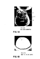
- Figs. 1A and 1B show electron micrographs of two solder pads; one immediately after evaporation and the other half an hour after the leaching melt at 280 ° C in a-102 flux.
- the indium cover 11 is visible on the vapor-deposited solder joint, as is the change in the volume of the solder joint due to the heating in the flux, which reflects the removal of the indium from the solder joint.
- the time dependence of the a-102 and TBC (triethanolamine-butyl cellosolve) reactions was determined at 280 ° C at 50:50 indium / lead solder joints.
- the a-102 flux was reacted at 280 0 with the vapor-deposited on the chips and solder pads with the same according to a first performed melting: A difference between the two could, as can be seen from Table IV, are not detected.
- Fig. 3 the time dependence of the leaching of indium by a-1 0 2 and TBC (triethanolamine / butyl cellosolve) flux is plotted. After a start-up time for the a-102 flux, a very rapid leaching takes place, the speed decreasing as the indium concentration decreases. The amount leached out by the TBC flux decreased at a constant rate.
- Figure 4 shows the time dependence of the leaching of indium by the a-102 flux at different temperatures, the 250 0 curve probably having the same shape as the 280 curve when additional points are measured. Note that the indium content after 5 minutes at 350 ° C is essentially the same as after half an hour at 280 ° C.
- the time in the experiments described above is the total time in the oven. 5 shows the thermal profile of an oven which has been heated to 280.degree. This was obtained by mounting the thermocouple in a flux beaker and determining the temperatures of the beaker placed in the oven. All conditions were similar to the experimental conditions. After 5 minutes The temperature is only 245 ° C, which is the start-up time that is shown in FIGS. 3 and 4 appears to explain ..
- the figures 6A and 6B show intermediate stages in the production of a modified solder connection of a chip 20 to a, conductor pattern 21 on a ceramic carrier 22.
- the integrated semiconductor chip 20, not shown, contains integrated circuits. It is covered with a first aluminum conductor pattern 23, parts of which are exposed via contact openings in the passivating layer 24, for example made of silicon dioxide.
- the contact points 4 (as in FIG. 1) are formed in contact with the underlying metallization 23 over each opening.
- a lead layer 10 and a tin layer 11A are deposited as double-layer solder connection points 9 on each contact point.
- This double-layer solder connection point 9 can be heated in order to fuse the tin layer 11A with the lead layer 10 to form a solder connection point 25 made of a 5:95 tin / lead alloy.
- the chip 20 is then placed relative to the ceramic substrate 22 to make solder connections 25 to the metallization 21 of the ceramic substrate 22 at the desired locations, and the units are bonded together by conventional heating.
- the voids between the chip 20 connected to the substrate 22 are filled with a-102 flux 3 and the assembly is heated at 350 ° C for leaching for 1/2 hour.
- the tin content in the alloy of the solder pads 25 was reduced to about 0.4% tin.
Landscapes
- Engineering & Computer Science (AREA)
- Computer Hardware Design (AREA)
- Microelectronics & Electronic Packaging (AREA)
- Power Engineering (AREA)
- Mechanical Engineering (AREA)
- Physics & Mathematics (AREA)
- Condensed Matter Physics & Semiconductors (AREA)
- General Physics & Mathematics (AREA)
- Electric Connection Of Electric Components To Printed Circuits (AREA)
- Wire Bonding (AREA)
Abstract
Description
Die Erfindung betrifft ein Verfahren zur in-situ Änderung' der Zusammensetzungen von Lötlegierungen mit einem Gehalt an Blei und einem Netzmittel, beispielsweise Zinn oder Indium. Bei diesem Verfahren wird der Bleigehalt in der Legierung der gelöteten Verbindung erhöht, was besonders bei der Halbleiterfertigung von Bedeutung ist.The invention relates to a method for in situ modification 'of the compositions of solder alloy containing lead and a wetting agent, such as tin or indium. With this method, the lead content in the alloy of the soldered connection is increased, which is particularly important in semiconductor production.
Es ist bekannt, daß reines Blei zur Herstellung von Lötverbindungen nicht geeignet ist, weil es nicht benetzend wirkt, was für gute Lötverbindungen unbedingt erforderlich ist. Gute Lötverbindungen werden beispielsweise mit Bleilegierungen, wie 95:5 Blei/Zinn oder 95:5 Blei/Indium erhalten.It is known that pure lead is not suitable for producing soldered connections because it does not have a wetting effect, which is absolutely necessary for good soldered connections. Good solder connections are obtained, for example, with lead alloys such as 95: 5 lead / tin or 95: 5 lead / indium.
Lötverbindungen aus reinem Blei oder Blei mit einem hohen Bleigehalt würden jedoch im Vergleich mit konventionellen Lötlegierungen ein 2- bis 3mal besseres Verhalten hinsichtlich der Ermüdung aufweisen. Auch würden Lötverbindungen aus im wesentlichen reinem Blei eine erhöhte Kriechfestigkeit unter Dauerbelastung verglichen mit der eines 50:50 Blei/ Indiumlots aufweisen. In diesem Zusammenhang werden auf die US-Patentschrift 3 380 821 und auf die Veröffentlichung von R. Herdzik et a. "Blinde Anschlußstellen für erhöhte Kriechbeständigkeit", IBM Technical Disclosure Bulletin, Vol. 20, Nr. 4, September 1977, Seite 1394 hingewiesen. Bisher ist kein vernünftiges Verfahren bekannt, Blei-Lötverbindungen ohne einen wesentlichen Gehalt an Netzmitteln, wie Zinn oder Indium herzustellen.Solder connections made of pure lead or lead with a high lead content would, however, exhibit 2 to 3 times better fatigue behavior compared to conventional solder alloys. Also, solder connections made of essentially pure lead would have an increased creep resistance under permanent load compared to that of a 50:50 lead / indium solder. In this connection, U.S. Patent 3,380,821 and the publication by R. Herdzik et a. "Blind connection points for increased creep resistance", IBM Technical Disclosure Bulletin, Vol. 20, No. 4, September 1977, page 1394. To date, no reasonable method is known for producing lead solder connections without a substantial content of wetting agents, such as tin or indium.
Aufgabe der Erfindung ist deshalb die Bereitstellung eines Verfahrens zur in-situ Änderung der Zusammensetzungen von Lötlegierungen mit einem Gehalt an Blei und einem Netzmittel.The object of the invention is therefore to provide a method for changing the compositions of solder alloys containing lead and a wetting agent in situ.
Die Aufgabe der Erfindung wird gelöst durch ein Verfahren der eingangs genannten Art, daß dadurch gekennzeichnet ist,. daß die Lötlegierungen in geschmolzener Form eine ausreichende Zeit lang mit einem Lötflußmittel erhitzt werden, um den Gehalt an Netzmittel in der geschmolzenen Lötlegierung herabzusetzen.The object of the invention is achieved by a method of the type mentioned at the outset, which is characterized in that. that the molten solder alloy is heated with a solder flux for a sufficient time to reduce the level of wetting agent in the molten solder alloy.
Vorteilhafte Ausgestaltungen der Erfindung sind in den Unteransprüchen angegeben. Mit dem erfindungsgemäßen Verfahren können Lötverbindungen mit einer erhöhten Beständigkeit hinsichtlich Ermüdung und auch mit erhöhter Kriechfestigkeit im Vergleich mit bisher bekannten Lötlegierungen erhalten werden. Die Zusammensetzung der Lötlegierung kann dabei nach Herstellung der Verbindungsstelle durch die Einwirkung eines geeigneten Lötflußmittels geändert werden, beispielsweise kann'der Bleigehalt der Lötverbindungen auf einen gewünschten Wert erhöht werden.Advantageous embodiments of the invention are specified in the subclaims. With the method according to the invention, soldered joints with increased resistance to fatigue and also with increased creep resistance can be obtained compared to previously known soldering alloys. The composition of the solder alloy can be changed after the connection point has been produced by the action of a suitable soldering flux, for example the lead content of the solder connections can be increased to a desired value.
Die Erfindung wird anhand der Figuren und der Beschreibung näher erläutert.The invention is explained in more detail with reference to the figures and the description.
- Fig. 1 ist ein vergrößerter Querschnitt einer Struktur, die bei der Herstellung eines Lötanschlusses erhalten wird.1 is an enlarged cross section of a structure obtained in making a solder joint.
- Fign. 1A sind Elektronenmikroskopaufnahmen bei 700facher und 1B Vergrößerung und einem Winkel von 60° der Struktur von Fig. 1 und einer Lötanschlußstelle, die erfindungsgemäß ausgelaugt wurde.Fig. 1A are electron micrographs at 700x and 1B magnification and an angle of 60 ° of the structure of FIG. 1 and a solder connection point which was leached out according to the invention.
- Fig. 2 ist ein binäres Phasendiagramm von Blei/Indium in Gleichgewicht.Figure 2 is a binary phase diagram of lead / indium in equilibrium.
- In Fig. 3 ist das Auslaugen von Indium aus einer 50:50 Indium/Blei-Lötanschlußstelle mit Abhängigkeit von der Zeit dargestellt.3 shows the leaching of indium from a 50:50 indium / lead solder connection with time.
- In Fig. 5 ist das thermische Profil eines Ofens, der auf 280 °C gehalten wird, dargestellt.5 shows the thermal profile of an oven which is kept at 280.degree.
- Fign. 6A und zeigen den Zustand von Lötverbindungen wäh-6B rend der Erhöhung des Gehalts an Blei, wie sie in der Halbleiterfertigung angewendet werden.Fig. 6A and 6B show the condition of solder joints during the increase in lead content as used in semiconductor manufacturing.
Es wurde gefunden, daß der Bleigehalt in Lötverbindungen aus einer Bleilegierung durch Modifizieren derselben erhöht werden kann, insbesondere bei einem Verfahren, bei dem die integrierten Halbleiterchips vor dem Auflöten auf die Substrate gewendet und dann aufgelötet werden. Zur Ausbildung von Lötverbindungen dieser Art werden konventionelle Lote, beispielsweise 95:5 Blei/Zinn und 95:5 Blei/Indium oder 50:50 Blei/Indium Lote verwendet, und anschließend wird das überschüssige Zinn oder Indium aus den resultierenden Verbindungen mit einem Flußmittel, welches wenigstens eine Harzsäure enthält, die aus der Gruppe der Monocarbonsäuren eines alkylierten Hydrophenanthrengerüsts mit der empirischen Formel C19H20COOH gewählt ist, entfernt. Auf diese Weise wird durch das Flußmittel bei erhöhten Temperaturen der Zinngehalt einer 95:5 Blei/Zinn-Lötverbindung auf weniger als 1 Gew.% erniedrigt. Indium reagiert noch leichter und kann aus einer Blei/Indium-Lötverbindung noch leichter ausgelaugt werden.It has been found that the lead content in solder connections made from a lead alloy can be increased by modifying them, in particular in a method in which the integrated semiconductor chips are turned onto the substrates before soldering and then soldered on. Conventional solders, for example 95: 5 lead / tin and 95: 5 lead / indium or 50:50 lead / indium solders, are used to form solder connections of this type, and then the excess tin or indium from the resulting connections is fluxed, which contains at least one resin acid selected from the group of monocarboxylic acids of an alkylated hydrophenanthrene skeleton with the empirical formula C19H20COOH. In this way, the flux reduces the tin content of a 95: 5 lead / tin solder joint to less than 1% by weight at elevated temperatures. Indium reacts even more easily and can be leached out even more easily from a lead / indium solder connection.
In der Mehrzahl der beschriebenen Experimente werden Halbleiterchips 1 verwendet, die nachfolgend als integrierte Halbleiterchips bezeichnet werden (Fig. 1) und aus einer ersten Aluminiummetallisierung 2, einer Siliciumdioxidschicht 3 und einer Kontaktstelle 4 bestehen, wobei letztere aus einer 200 nm dicken Chromschicht 5, einer 1000 nm dicken Kupferschicht 6 mit einer anfänglichen, etwa 80 nm dicken Schicht einer Chromkupferphase und einer 140 nm dicken Goldschicht 8 gebildet wird. Ein Beispiel dieser Art ist in Fig. 1 der IBM Technical Disclosure Bulletin-Veröffentlichung "Entfernungsverfahren" von C. Johnson et al., in Vol. 20, Nr. 6, . November 1977, auf den Seiten 2209 bis 2210 beschrieben. Jedes integrierte Halbleiterchip enthält 121 solcher Kontaktstellen 4.In the majority of the experiments described,
Wafer, welche integrierte Halbleiterchips dieser Art enthalten, werden nachfolgend als integrierte Halbleiterwafer bezeichnet, wobei jeder Wafer einige 100 integrierte Halbleiterchips enthält. Die Lötanschlußstelle 9 wurde auf die Kontaktstellen 4 in einer Höhe von 0,1143 mm durch eine Maske aufgedampft. Wegen des höheren Dampfdrucks von Blei wird dieses zuerst in einer Schicht 10 aufgedampft, und anschließend erfolgt das Aufdampfen von Indium in einer Schicht 11. Die Form der aufgedampfen Lötanschlußstellen war die eines Kegelstumpfs. Der Ausdruck "Nachträgliches Benetzen", der hier verwendet wird, bezeichnet ein Aufschmelzen zur Modifizierung der Lötanschlußstellen, beispielsweise um die beiden Schichten der Lötanschlußstelle 4 miteinander zu verschmelzen und dadurch das Netzmittel, die Indium-/oder Zinnschicht 11, dem Blei als Lötlegierung einzuverleiben.Wafers which contain integrated semiconductor chips of this type are referred to below as integrated semiconductor wafers, each wafer containing some 100 integrated semiconductor chips. The
Die Zusammensetzungen der Lötlegierungen einschließlich aller Lötanschlußstellen wurden durch Messung ihrer Schmelzpunkte unter Anwendung eines Perkin-Elmer-Differentialkalorimeters (Differential Scanning Calorimetry, abgekürzt DSC) bestimmt. Weil experimentell leichter durchführbar, wurden bei den Messungen die Abkühlungskurven verwendet. Aus bekannten Zusammensetzungen wurden Standards hergestellt und unter den gleichen Bedingungen wie die Lötlegierungen und die Lötanschlußstellen unter Verwendung der gleichen Materialmengen untersucht.The compositions of the solder alloys, including all solder joints, were determined by measuring their melting points using a Perkin-Elmer differential calorimeter (DSC). Because experimentally easier to carry out, the cooling curves were used in the measurements. Standards were made from known compositions and tested under the same conditions as the solder alloys and the solder joints using the same amounts of material.
Die Mehrzahl der Experimente wurde in einem Rohrofen einer Stickstoffatmosphäre durchgeführt. Die Proben wurden in ein Becherglas gegeben, mit dem auslaugenden Flußmittel bedeckt und auf einer Glasplatte, an der ein Thermoelement befestigt war, in den Ofen gestellt.The majority of the experiments were carried out in a tube furnace in a nitrogen atmosphere. The samples were placed in a beaker, covered with the leaching flux and on a glass plate to which a thermocouple was attached was put in the oven.
Die Flußmittel, welche verwendet wurden, waren von Alpha Metals, beispielsweise a-102-1500 mit einem Zusatz von 20 % Isopropylalkohol (IPA), bezogen auf das Gewicht von . a-102-1500, und a-100-40. Es wurden auch wasserhelles Kolophonium und ein wasserlösliches Flußmittel mit der Bezeichnung TBC, welches aus 50 Vol.% Triäthanolamin und 50 Vol.% Butylglykol (Butylcellosolve) bestand, verwendet. Das a-102-1500-Flußmittel wird nachfolgend als a-102 bezeichnet, wobei die zweite Hälfte der Zahlenangabe (1500) die Viskosität des Flußmittels angibt. In ähnlicher Weise wird das a-100-40-Flußmittel nachfolgend als a-104 bezeichnet. Das a-102-Flußmittel wird als 68 Gew.%ige Lösung von Abietinsäure in Benzylalkohol und das a-104-Flußmittel als 40 Gew.%ige Lösung von Abietinsäure in Isopropanol geliefert. Wasserhelles Kolophonium ist eine Harzsäure vom Typ der Monocarbonsäuren des alkylierten Hydrophenanthrengerüsts mit einer empirischen Formel C19H29COOH.The fluxes used were from Alpha Metals, for example a-102-1500 with an addition of 20% isopropyl alcohol (IPA) by weight of. a- 102-1500, and a-100-40. Water-white rosin and a water-soluble flux called TBC, which consisted of 50% by volume of triethanolamine and 50% by volume of butyl glycol (butyl cellosolve), were also used. The a-102-1500 flux is referred to below as a-102, with the second half of the number (1500) indicating the viscosity of the flux. Similarly, the a-100-40 flux is referred to below as a-104. The a-102 flux is supplied as a 68% by weight solution of abietic acid in benzyl alcohol and the a-104 flux as a 40% by weight solution of abietic acid in isopropanol. Rosin is a rosin acid of the monocarboxylic acid type of the alkylated hydrophenanthrene skeleton with an empirical formula C 19 H 29 COOH.
In den beiden ersten Experimenten wurden zwei integrierte Halbleiterwafer, die 200 integrierte Halbleiterchips enthielten, verwendet und einem vollständigen Verfahren mit aufeinanderfolgender Abscheidung von 50:50 Indium/Blei-Anschlüssen 9, d.h. einer Bleischicht 10 und einer Indiumschicht 11 (Fign. 1 und 1A) unterworfen. Auf die Hälfte eines Wafers wurde über den Lötanschlüssen das a-102-Flußmittel aufgetragen, diese wurden zwei Minuten lang bei 275 °C aufgeschmolzen, was nachfolgend mit auslaugendem Aufschmelzen bezeichnet wird. Nach dem auslaugenden Aufschmelzen wurde dieser Teil der Waferhälfte zwei Minuten lang bei 275 °C in einer Stickstoffatmosphäre einer zweiten Aufschmelzbehandlung unterworfen. Der restliche halbe Wafer wurde beiden Aufschmelzbehandlungen in umgekehrter Reihenfolge, d.h., zuerst einer zwei Minuten dauernden Aufschmelzbehandlung bei 275 °C in Stickstoffatmosphäre und dann einer zwei Minuten dauernden Aufschmelzbehandlung mit a-102-Flußmittel bei 275 °C unterworfen.In the first two experiments, two integrated semiconductor wafers, which contained 200 integrated semiconductor chips, were used and a complete process with successive deposition of 50:50 indium /
Die Ergebnisse sind in der nachfolgenden Tabelle I aufgetragen. Es ist ersichtlich, daß die Aufschmelzbehandlung.in Stickstoffatmosphäre keinen Einfluß auf die Indiumkonzentration ausübt, während die Indiumkonzentration durch das auslaugende Aufschmelzen mit a-102-Flußmittel reduziert wird.

Im nächsten Versuch wurden einzelne Wafersegmente, welche je drei integrierte Halbleiterchips enthielten (aus dem integrierten Halbleiterwafer abgeteilt), in ein Becherglas gegeben und mit verschiedenen Flußmitteln für Reaktionszeiten und Temperatur bedeckt. Zusätzlich wurde eine Kontrollprobe angewendet, bei der die Lötanschlußstelle nur in Stickstoffatmosphäre aufgeschmolzen wurde. In jedem Fall hatten die Proben eine Kontaktstelle 4. Es wurden auch Proben angewendet, bei denen die Lötanschlußstelle 9 direkt auf eine blanke Siliciumsubstratoberfläche aufgedampft war. Die nachfolgende Tabelle II zeigt den Effekt des Auslaugens von Indium durch verschiedene Flußmittel während einer halben Stunde bei 280 °C.In the next experiment, individual wafer segments, each containing three integrated semiconductor chips (separated from the integrated semiconductor wafer), were placed in a beaker and with different fluxes for reaction times and temperature covered. In addition, a control sample was used in which the solder connection point was only melted in a nitrogen atmosphere. In each case, the samples had a
Die Erfindung gestattet auch die Reparatur oder den Ersatz eines oder mehrerer Chips einer Vielzahl von Chips, die mit einem Träger, beispielsweise einem mehrschichtigen Keramiksubstrat durch ein hochschmelzendes Lot, beispielsweise ein 85 % Blei/15 % Indiumlot (Fig. 2) verbunden sind. Bei dieser Anwendung kann das Chip, weil die Lötstellen außerordentlich klein sind, mechanisch abgetrennt oder von dem Träger entfernt werden. Anschließend wird ein neues Chip auf der freigewordenen Stelle angeordnet, wobei das Chip mit einem niedrigschmelzenden Lot, beispielsweise einem 55 % Blei/45 % Indiumlot versehen ist, und die Einheit wird auf eine Temperatur (beispielsweise 250 °C, Fig. 2), die über dem Schmelzpunkt des 55 Blei/45 Indiumlots, aber unter dem Schmelzpunkt des 85 Blei/15 Indiumlots liegt, erhitzt, um die Zusammensetzung 55 Blei/45 Indium isothermisch in 85 Blei/15 Indium zu ändern, d.h., um das Lot in dem Solidusteil des Phasendiagramms zu positionieren. Auf diese Weise können einzelne Chips auf einer Anordnung mit vielen Chips ersetzt werden, ohne daß die Lötstellen der übrigen Chips aufgeschmolzen werden müssen.

In den Fign. 1A und 1B sind Elektronenmikroskopaufnahmen zweier Lötanschlußstellen gezeigt; eine unmittelbar nach dem Aufdampfen und die andere eine halbe Stunde nach dem auslaugenden Aufschmelzen bei 280 °C in a-102 Flußmittel. Die Indiumbedeckung 11 ist auf der aufgedampften Lötanschlußstelle sichtbar, wie auch die Änderung des Volumens der Lötanschlußstelle durch das Erhitzen in dem Flußmittel, welche die Abnahme des Indiums aus der Lötstelle wiederspiegelt.In Figs. 1A and 1B show electron micrographs of two solder pads; one immediately after evaporation and the other half an hour after the leaching melt at 280 ° C in a-102 flux. The
Die Temperaturabhängigkeit der Entfernung von Indium durch Auslaugen aus 50:50 Indium/Blei Lötanschlußstellen ist in der nachfolgenden Tabelle III gezeigt.


In Tabelle III wurden alle Chips eine halbe Stunde auf den angegebenen Temperaturen gehalten. Die gleichen Ergebnisse sind in dem Indium-Phasendiagramm in Fig. 2 aufgetragen, welches graphisch die Abnahme von Indium bei 280 °C und 250 °C zeigt.In Table III, all chips were held at the indicated temperatures for half an hour. The same results are plotted in the indium phase diagram in Fig. 2, which graphically shows the decrease in indium at 280 ° C and 250 ° C.
Die Zeitabhängigkeit der a-102- und TBC (TriäthanolaminButylcellosolve)-Reaktionen wurde bei 280 °C an 50:50 Indium/Blei-Lötanschlußstellen bestimmt. Das a-102-Flußmittel wurde bei 2800 mit den auf den Chips aufgedampften Lötanschlußstellen und mit denselben nach einem zuerst durchgeführten Aufschmelzen umgesetzt: Ein Unterschied zwischen den beiden konnte, wie aus Tabelle IV ersichtlich ist, nicht festgestellt werden.


In Fig. 4 ist die Zeitabhängigkeit des Auslaugens von Indium durch das a-102 Flußmittel bei verschiedenen Temperaturen dargestellt, wobei die 2500-Kurve wahrscheinlich die gleiche Form wie die 280 -Kurve haben dürfte, wenn zusätzliche Punkte gemessen werden. Es sei bemerkt, daß der Indiumgehalt nach 5 Min. bei 350 °C im wesentlichen der gleiche ist wie nach einer halben Stunde bei 280 °C.Figure 4 shows the time dependence of the leaching of indium by the a-102 flux at different temperatures, the 250 0 curve probably having the same shape as the 280 curve when additional points are measured. Note that the indium content after 5 minutes at 350 ° C is essentially the same as after half an hour at 280 ° C.
Die Zeit in den zuvor beschriebenen Experimenten ist die Gesamtzeit im Ofen. In Fig. 5 ist das thermische Profil eines Ofens, der auf 280 °C erhitzt ist, dargestellt. Dieses wurde erhalten, indem man das Thermoelement in einem Becherglas mit Flußmittel befestigte und die Temperaturen des in den Ofen gestellten Becherglases bestimmte. Alle Bedingungen waren den experimentellen Bedingungen ähnlich. Nach 5 Minuten beträgt die Temperatur nur 245 °C, was die Anlaufzeit, die in den Fign. 3 und 4 angegeben ist, zu erklären scheint..The time in the experiments described above is the total time in the oven. 5 shows the thermal profile of an oven which has been heated to 280.degree. This was obtained by mounting the thermocouple in a flux beaker and determining the temperatures of the beaker placed in the oven. All conditions were similar to the experimental conditions. After 5 minutes The temperature is only 245 ° C, which is the start-up time that is shown in FIGS. 3 and 4 appears to explain ..
Eine Überprüfung der ungefähren Löslichkeit von Indium in Abietinsäure wurde durchgeführt, indem 500 mg Stücke von, reinem Indium in bekannte Gewichtsmengen von Abietinsäure gegeben wurde. Die Ergebnisse für 200 °C und 280 °C sind in der nachfolgenden Tabelle V angegeben.

Indium und Abietinsäure wurden durch Differentialkalorimetermessungen und Differentialthermoanalyse analysiert, Ergebnisse nicht überzeugend.Indium and abietic acid were analyzed by differential calorimeter measurements and differential thermal analysis, results not convincing.
Für die Werte in dieser Tabelle wurde der Gewichtsverlust von Indium bestimmt und die Löslichkeiten berechnet. Es sind zwei Löslichkeitswerte angegeben, bezogen auf das anfängliche und das Endgewicht des Harzes, weil beim'Erhitzen ein Verlust an Abietinsäure auftritt. Der Löslichkeitsunterschied zwischen 200 und 280 °C ist nicht groß genug, um die Ergebnisse der Auslaugversuche, die in Tabelle III angegeben und in Fig. 2 aufgezeichnet sind, zu erklären.The weight loss of indium was determined for the values in this table and the solubilities were calculated. Two solubility values are given, based on the initial and the final weight of the resin, because there is a loss of abietic acid when heated. The difference in solubility between 200 and 280 ° C is not large enough to explain the results of the leaching tests given in Table III and recorded in Fig. 2.
Da die Löslichkeit von Indium bei 280 °C in Kolophonium in der Größenordnung von 10 % liegt, würde eine Herabsetzung des Kolophoniums in dem Flußmittel die entfernte Menge Indium auch herabsetzen. Die Auswirkungen der Änderung des Gewichtsververhältnisses von Kolophonium zu dem 50:50 Indium/Bleitlot wurden bei 280 °C untersucht (tatsächliche Temperatur der Probe 285 °C). Es wurde Kolophonium im Verhältnis 1:1 und 5:1 zu dem 50:50 Indium/Bleilot verwendet. Ein 200 mg Stück von 50:50 Indium/Blei wurde in ein Becherglas mit dem gewünschten Gewicht an Kolophonium gegeben. Die Ergebnisse sind in Tabelle VI aufgezeichnet.

Wie zu erwarten ist, ist die Herabsetzung des Indiumgehalts in der Legierung um so größer, je größer der Kolophoniumanteil ist. Zum Vergleich werden Ergebnisse an Chiplötstellen bei Anwendung von Kontaktanschlußstellen gezeigt. Das Sollverhältnis von Kolophonium zu 50:50 Indium/Blei war 200:1, welches sich um + 25 % geändert haben mochte. Mit der größeren Menge an Kolophonium, die auf den Chips vorhanden war, wurde eine viel größere Abnahme an Indium in einer viel kürzeren Zeit erreicht.As can be expected, the greater the rosin content, the greater the reduction in the indium content in the alloy. For comparison, results are shown at chip solder joints when using contact connection points. The target ratio of rosin to 50:50 indium / lead was 200: 1, which may have changed by + 25%. With the greater amount of rosin present on the chips, a much greater decrease in indium was achieved in a much shorter time.
Ein weiterer Weg, diese Ergebnisse darzustellen, ist, die Konzentration von Indium in dem Kolophonium anzugeben. Diese Ergebnisse sind in Tabelle VII zusammengestellt.

Die Ergebnisse sind dargestellt als Zusammensetzungen unter Verwendung der Endgewichte von Kolophonium. Das Kolophonium war höchst wahrscheinlich für das 1:1 Gewichtsverhältnis nach 15 Stunden an Indium gesättigt oder nahezu gesättigt. Für das 5:1 Verhältnis nach 12 Stunden war das Kolophonium nicht gesättigt und bei den Chips war nur eine kleine Menge Indium in Lösung, obgleich nahezu alles Indium aus den Lötanschlußstellen entfernt war. Daraus ist klar zu erkennen, daß, je größer das Gewichtsverhältnis von Kolophonium zu 50:50 Indium/Bleilegierung ist, desto größer auch, wie zu erwarten ist, der Gehalt an gelöstem Indium ist.The results are presented as compositions using the final weights of rosin. The rosin was most likely saturated or nearly saturated for the 1: 1 weight ratio after 15 hours of indium. For the 5: 1 ratio after 12 hours, the rosin was not saturated and only a small amount of indium was in solution in the chips, although almost all of the indium was removed from the solder pads. From this it can be clearly seen that the greater the weight ratio of rosin to 50:50 indium / lead alloy, the greater, as can be expected, the content of dissolved indium.
Ein Chip mit 5:95 Zinn/Blei wurde 1/2 Stunde lang auf 350 °C erhitzt, und der Zinngehalt wurde mit einem -102 Flußmittel von 5 % auf 3/4 % reduziert. Die Ergebnisse in Tabelle 8 nach der Atomabsorption (AA) zeigen die Daten für kürzere Erhitzungszeiten.

Obgleich eine Diskrepanz bei Legierungen mit einem höheren Zinngehalt vorliegt, ist ersichtlich, daß Zinn auch aus Zinn/ Blei-Loten durch Lötflußmittel auf der Basis von Kolophonium ausgelaugt wird. Chips mit einem Sollwert 5:95 Zinn/Blei wurden drei Erhitzungszyklen unterworfen unter Anwendung des a-102-1500 Flußmittels mit 20 % Isopropylalkohol, wobei jedesmal ein neues Flußmittel angewendet wurde. Der Zinngehalt der Zusammensetzung änderte sich von 4,5 % Zinn auf 3,5 % Zinn, was mit dem Differentialkalorimeter bestimmt wurde.Although there is a discrepancy in alloys with a higher tin content, it can be seen that tin is also leached from tin / lead solders by rosin-based soldering fluxes. A setpoint 5:95 tin / lead chips were subjected to three heating cycles using the a-102-1500 flux with 20% isopropyl alcohol, each time using a new flux. The tin content of the composition changed from 4.5% tin to 3.5% tin, which was determined with the differential calorimeter.
Die Fign. 6A und 6B zeigen Zwischenstufen bei der Herstellung einer modifizierten Lötverbindung eines Chips 20 zu einem , Leiterzugmuster 21 auf einem Keramikträger 22. Das integrierte Halbleiterchip 20 enthält, nicht gezeigt, integrierte Schaltkreise. Es ist bedeckt mit einem ersten Aluminiumleiterzugmuster 23, von dem Teile über Kontaktöffnungen in der passivierenden Schicht 24, beispielsweise aus Siliciumdioxid, freigelegt sind. Die Kontaktstellen 4 (wie in Fig. 1) werden über jeder Öffnung in Kontakt mit der darunter liegenden Metallisierung 23 gebildet. Aufeinanderfolgend werden auf jeder Kontaktstelle eine Bleischicht 10 und eine Zinnschicht 11A als doppelschichtige Lötanschlußstelle 9 abgeschieden. Diese doppelschichtige Lötanschlußstelle 9 kann erhitzt werden, um die Zinnschicht 11A mit der Bleischicht 10 unter Ausbildung einer Lötanschlußstelle 25 aus einer 5:95 Zinn/Blei-Legierung zu verschmelzen. Das Chip 20 wird dann relativ zum Keramiksubstrat 22 angeordnet zur Herstellung von Lötverbindungen 25 mit der Metallisierung 21 des Keramiksubstrats 22 an den gewünschten Stellen, und die Einheiten werden durch konventionelles Erhitzen miteinander verbunden. Die Hohlräume zwischen dem Chip 20, das mit dem Substrat 22 verbunden ist, werden mit a-102 Flußmittel 3 gefüllt, und die Anordnung wird 1/2 Stunde lang bei 350 °C zum Auslaugen erhitzt. Der Zinngehalt in der Legierung der Lötanschlußstellen 25 wurde auf etwa 0,4 % Zinn herabgesetzt.The figures 6A and 6B show intermediate stages in the production of a modified solder connection of a
Claims (6)
dadurch gekennzeichnet,
daß die Lötlegierungen in geschmolzener Form eine ausreichende Zeit lang mit einem Lötflußmittel erhitzt werden, um den Gehalt an Netzmittel in der geschmolzenen Lötlegierung herabzusetzen.1. Process for in-situ changing of the composition of solder alloys containing lead and a wetting agent,
characterized,
that the molten solder alloy is heated with a solder flux for a sufficient time to reduce the level of wetting agent in the molten solder alloy.
dadurch gekennzeichnet,
daß die Lötlegierungen mit einem Gehalt an Zinn oder Indium in geschmolzener Form eine ausreichende Zeit lang mit wenigstens einem Lötflußmittel aus der Gruppe der Monocarbonsäuren eines alkylierten Hydrophenanthrengerüsts mit der allgemeinen Formel C19H29COOH erhitzt werden, um den Gehalt an Zinn oder Indium in der geschmolzenen Lötlegierung herabzusetzen.2. The method according to claim 1
characterized,
that the soldering alloys containing tin or indium in molten form are heated for a sufficient time with at least one soldering flux from the group of the monocarboxylic acids of an alkylated hydrophenanthrene skeleton with the general formula C 19 H 29 COOH in order to reduce the content of tin or indium in the to reduce molten solder alloy.
dadurch gekennzeichnet,
daß die Säuren in Form wasserhellen Kolophoniums angewendet werden.3. The method according to claim 2, characterized in
characterized,
that the acids are used in the form of water-bright rosin.
dadurch gekennzeichnet,
daß die Lötlegierungen bei Temperaturen oberhalb ihres Schmelzpunkts zwischen den miteinander zu verbindenden Teilen einer integrierten Schaltung aufgetragen und in geschmolzener Form eine ausreichende Zeit lang mit dem Lötflußmittel behandelt werden, um den Gehalt an Zinn oder Indium in der Lötlegierung herabzusetzen.4. The method according to claims 1 to 3,
characterized,
that the solder alloys are applied at temperatures above their melting point between the parts of an integrated circuit to be connected to one another and are treated in molten form with the solder flux for a sufficient time to reduce the content of tin or indium in the solder alloy.
dadurch gekennzeichnet,
daß die Lötlegierung zur Entfernung von Zinn oder Indium mit dem Lötflußmittel eine ausreichende Zeit lang auf einer bestimmten Temperatur gehalten wird, um die Zusammensetzung der geschmolzenen Lötlegierung bei der gewählten Temperatur so zu ändern, daß sie auf einem Punkt der Solidus-Kurve des Phasendiagramms der Legierung liegt.5. The method according to claims 1 to 4,
characterized,
that the soldering alloy for removing tin or indium with the soldering flux is held at a certain temperature for a sufficient time to change the composition of the molten soldering alloy at the selected temperature so that it is on a point on the solidus curve of the phase diagram of the alloy lies.
dadurch gekennzeichnet,
daß das Lötflußmittel auf Lötlegierungen angewendet wird, die ein integriertes Halbleiterchip mit einem dielektrischen Substrat verbinden, dessen Schaltkreismuster auf die Schaltkreiskonfiguration des Halbleiterchips abgestimmt ist.6. The method according to claims 1 to 5,
characterized,
that the soldering flux is applied to solder alloys that connect an integrated semiconductor chip to a dielectric substrate, the circuit pattern of which is matched to the circuit configuration of the semiconductor chip.
Applications Claiming Priority (2)
| Application Number | Priority Date | Filing Date | Title |
|---|---|---|---|
| US94422478A | 1978-09-20 | 1978-09-20 | |
| US944224 | 1978-09-20 |
Publications (2)
| Publication Number | Publication Date |
|---|---|
| EP0009131A1 true EP0009131A1 (en) | 1980-04-02 |
| EP0009131B1 EP0009131B1 (en) | 1981-12-23 |
Family
ID=25481021
Family Applications (1)
| Application Number | Title | Priority Date | Filing Date |
|---|---|---|---|
| EP79103107A Expired EP0009131B1 (en) | 1978-09-20 | 1979-08-23 | Process for in situ modification of solder alloy compositions |
Country Status (5)
| Country | Link |
|---|---|
| EP (1) | EP0009131B1 (en) |
| JP (1) | JPS5846176B2 (en) |
| CA (1) | CA1122856A (en) |
| DE (1) | DE2961610D1 (en) |
| IT (1) | IT1122873B (en) |
Cited By (4)
| Publication number | Priority date | Publication date | Assignee | Title |
|---|---|---|---|---|
| EP0068091A2 (en) * | 1981-06-30 | 1983-01-05 | International Business Machines Corporation | Method for connecting a semiconductor chip to a substrate and such connection |
| EP0073383A2 (en) * | 1981-09-02 | 1983-03-09 | Hitachi, Ltd. | Semiconductor device having external electrodes bonded to electrodes on a semiconductor substrate and method of fabricating such a semiconductor device |
| US4498096A (en) * | 1981-01-30 | 1985-02-05 | Motorola, Inc. | Button rectifier package for non-planar die |
| EP0365768A1 (en) * | 1988-10-17 | 1990-05-02 | International Business Machines Corporation | Flux composition and method of decreasing tin content in lead/tin solder joints |
Families Citing this family (2)
| Publication number | Priority date | Publication date | Assignee | Title |
|---|---|---|---|---|
| US5007163A (en) * | 1990-04-18 | 1991-04-16 | International Business Machines Corporation | Non-destructure method of performing electrical burn-in testing of semiconductor chips |
| CN105759522B (en) * | 2016-05-11 | 2019-01-22 | 深圳市华星光电技术有限公司 | The broken wire repair method of TFT substrate |
Citations (3)
| Publication number | Priority date | Publication date | Assignee | Title |
|---|---|---|---|---|
| US2043573A (en) * | 1934-05-26 | 1936-06-09 | American Smelting Refining | Process for recovering tin |
| US3380821A (en) * | 1965-10-21 | 1968-04-30 | Gen Motors Corp | Heat treatable creep resistant solder alloy |
| US3478414A (en) * | 1967-05-05 | 1969-11-18 | Ibm | Water white rosin flux in benzyl alcohol solution |
-
1979
- 1979-07-27 CA CA332,645A patent/CA1122856A/en not_active Expired
- 1979-08-14 JP JP54102850A patent/JPS5846176B2/en not_active Expired
- 1979-08-23 DE DE7979103107T patent/DE2961610D1/en not_active Expired
- 1979-08-23 EP EP79103107A patent/EP0009131B1/en not_active Expired
- 1979-08-29 IT IT25326/79A patent/IT1122873B/en active
Patent Citations (3)
| Publication number | Priority date | Publication date | Assignee | Title |
|---|---|---|---|---|
| US2043573A (en) * | 1934-05-26 | 1936-06-09 | American Smelting Refining | Process for recovering tin |
| US3380821A (en) * | 1965-10-21 | 1968-04-30 | Gen Motors Corp | Heat treatable creep resistant solder alloy |
| US3478414A (en) * | 1967-05-05 | 1969-11-18 | Ibm | Water white rosin flux in benzyl alcohol solution |
Non-Patent Citations (1)
| Title |
|---|
| FEINWERKTECHNIK, BAND 76, 1972, Heft 3, Seiten 130-134 Munchen, DE. P.A. AINSWORTH: "Beeinflussung der mechanischen Eigenschaften von Weichlotverbindungen in elektronischen Ausrustungen" * Seiten 130-134 * * |
Cited By (6)
| Publication number | Priority date | Publication date | Assignee | Title |
|---|---|---|---|---|
| US4498096A (en) * | 1981-01-30 | 1985-02-05 | Motorola, Inc. | Button rectifier package for non-planar die |
| EP0068091A2 (en) * | 1981-06-30 | 1983-01-05 | International Business Machines Corporation | Method for connecting a semiconductor chip to a substrate and such connection |
| EP0068091A3 (en) * | 1981-06-30 | 1984-11-14 | International Business Machines Corporation | Method for connecting a semiconductor chip to a substrate and such connection |
| EP0073383A2 (en) * | 1981-09-02 | 1983-03-09 | Hitachi, Ltd. | Semiconductor device having external electrodes bonded to electrodes on a semiconductor substrate and method of fabricating such a semiconductor device |
| EP0073383A3 (en) * | 1981-09-02 | 1984-08-08 | Hitachi, Ltd. | Semiconductor device having external electrodes bonded to electrodes on a semiconductor substrate and method of fabricating such a semiconductor device |
| EP0365768A1 (en) * | 1988-10-17 | 1990-05-02 | International Business Machines Corporation | Flux composition and method of decreasing tin content in lead/tin solder joints |
Also Published As
| Publication number | Publication date |
|---|---|
| JPS5574160A (en) | 1980-06-04 |
| DE2961610D1 (en) | 1982-02-11 |
| CA1122856A (en) | 1982-05-04 |
| EP0009131B1 (en) | 1981-12-23 |
| IT7925326A0 (en) | 1979-08-29 |
| JPS5846176B2 (en) | 1983-10-14 |
| IT1122873B (en) | 1986-04-30 |
Similar Documents
| Publication | Publication Date | Title |
|---|---|---|
| DE69217617T2 (en) | Connection method using a solder consisting of multiple alternating gold and tin layers | |
| DE69837224T2 (en) | Electronic device connected to lead-free solder | |
| DE19823615B4 (en) | soldering flux | |
| DE69521762T2 (en) | Lead-free, low-melting solder with improved mechanical properties and objects associated with this solder | |
| DE69900894T2 (en) | Fat-free, lead-free alloy | |
| DE19545783B4 (en) | A method for specifying the suitability of an organic substance as a soldering flux and soldering method using the same | |
| DE69522993T2 (en) | Soldering flux and method | |
| DE2424857C2 (en) | Process for producing a soldered connection by reflow soldering | |
| DE10208635B4 (en) | Diffusion soldering station, composite of two parts connected via a diffusion soldering station and method for producing the diffusion soldering station | |
| DE60217199T2 (en) | Lead-free soft solder and soft solder connection | |
| DE69813701T2 (en) | Electrode structure of a silicon semiconductor device | |
| EP2456589B1 (en) | Lead free high temperature connection | |
| DE60300669T2 (en) | Lead-free soldering alloy | |
| DE3650544T2 (en) | Lead base alloys and use to reduce electromigration activity | |
| DE69022668T2 (en) | Electronic connections, methods of forming end connectors therefor and paste for forming the same. | |
| DE68906853T2 (en) | Flux composition and method for reducing the tin content in lead-tin solder joints. | |
| DE1627762A1 (en) | Method for manufacturing semiconductor components | |
| EP0009131B1 (en) | Process for in situ modification of solder alloy compositions | |
| DE19750104B4 (en) | Use of a solder paste for chip components | |
| DE4016384A1 (en) | ELECTRONIC CIRCUIT DEVICE | |
| DE60305119T2 (en) | Leach-resistant solder alloys for silver-based electrically conductive thick films | |
| DE19542043A1 (en) | Lead-free, low temperature alloy and method of forming a mechanically superior joint using this alloy | |
| DE2550275A1 (en) | PROCESS FOR CREATING BARRIERS FOR LOETZINN ON LADDER | |
| DE3720594C2 (en) | ||
| DE1752137B2 (en) | Process for soldering microminiaturized circuits and flux to carry out the process |
Legal Events
| Date | Code | Title | Description |
|---|---|---|---|
| PUAI | Public reference made under article 153(3) epc to a published international application that has entered the european phase |
Free format text: ORIGINAL CODE: 0009012 |
|
| AK | Designated contracting states |
Designated state(s): DE FR GB |
|
| 17P | Request for examination filed | ||
| GRAA | (expected) grant |
Free format text: ORIGINAL CODE: 0009210 |
|
| AK | Designated contracting states |
Designated state(s): DE FR GB |
|
| REF | Corresponds to: |
Ref document number: 2961610 Country of ref document: DE Date of ref document: 19820211 |
|
| PGFP | Annual fee paid to national office [announced via postgrant information from national office to epo] |
Ref country code: DE Payment date: 19890904 Year of fee payment: 11 |
|
| PGFP | Annual fee paid to national office [announced via postgrant information from national office to epo] |
Ref country code: GB Payment date: 19900704 Year of fee payment: 12 |
|
| PG25 | Lapsed in a contracting state [announced via postgrant information from national office to epo] |
Ref country code: DE Effective date: 19910501 |
|
| PGFP | Annual fee paid to national office [announced via postgrant information from national office to epo] |
Ref country code: FR Payment date: 19910726 Year of fee payment: 13 |
|
| PG25 | Lapsed in a contracting state [announced via postgrant information from national office to epo] |
Ref country code: GB Effective date: 19910823 |
|
| GBPC | Gb: european patent ceased through non-payment of renewal fee | ||
| PG25 | Lapsed in a contracting state [announced via postgrant information from national office to epo] |
Ref country code: FR Effective date: 19930430 |
|
| REG | Reference to a national code |
Ref country code: FR Ref legal event code: ST |
|
| PLBE | No opposition filed within time limit |
Free format text: ORIGINAL CODE: 0009261 |
|
| STAA | Information on the status of an ep patent application or granted ep patent |
Free format text: STATUS: NO OPPOSITION FILED WITHIN TIME LIMIT |