EP0004870A1 - Transversal filter with parallel inputs - Google Patents
Transversal filter with parallel inputs Download PDFInfo
- Publication number
- EP0004870A1 EP0004870A1 EP79100803A EP79100803A EP0004870A1 EP 0004870 A1 EP0004870 A1 EP 0004870A1 EP 79100803 A EP79100803 A EP 79100803A EP 79100803 A EP79100803 A EP 79100803A EP 0004870 A1 EP0004870 A1 EP 0004870A1
- Authority
- EP
- European Patent Office
- Prior art keywords
- input
- evaluation
- shift register
- gate
- input signal
- Prior art date
- Legal status (The legal status is an assumption and is not a legal conclusion. Google has not performed a legal analysis and makes no representation as to the accuracy of the status listed.)
- Granted
Links
- 238000011156 evaluation Methods 0.000 claims abstract description 79
- 230000015654 memory Effects 0.000 claims abstract description 17
- 239000004065 semiconductor Substances 0.000 claims abstract description 9
- 230000003068 static effect Effects 0.000 claims abstract description 3
- 238000012546 transfer Methods 0.000 claims description 34
- 239000000758 substrate Substances 0.000 claims description 12
- 238000011144 upstream manufacturing Methods 0.000 claims 1
- 230000001419 dependent effect Effects 0.000 abstract 1
- 230000006870 function Effects 0.000 abstract 1
- 238000009792 diffusion process Methods 0.000 description 9
- 238000000034 method Methods 0.000 description 7
- 230000005669 field effect Effects 0.000 description 5
- 238000011161 development Methods 0.000 description 3
- 101150110971 CIN7 gene Proteins 0.000 description 2
- 101150110298 INV1 gene Proteins 0.000 description 2
- 101100397044 Xenopus laevis invs-a gene Proteins 0.000 description 2
- 239000002800 charge carrier Substances 0.000 description 2
- 238000010586 diagram Methods 0.000 description 2
- 238000006073 displacement reaction Methods 0.000 description 2
- 239000013589 supplement Substances 0.000 description 2
- MAYZWDRUFKUGGP-VIFPVBQESA-N (3s)-1-[5-tert-butyl-3-[(1-methyltetrazol-5-yl)methyl]triazolo[4,5-d]pyrimidin-7-yl]pyrrolidin-3-ol Chemical compound CN1N=NN=C1CN1C2=NC(C(C)(C)C)=NC(N3C[C@@H](O)CC3)=C2N=N1 MAYZWDRUFKUGGP-VIFPVBQESA-N 0.000 description 1
- 229910004298 SiO 2 Inorganic materials 0.000 description 1
- 230000005540 biological transmission Effects 0.000 description 1
- 230000000903 blocking effect Effects 0.000 description 1
- 239000000969 carrier Substances 0.000 description 1
- 238000006243 chemical reaction Methods 0.000 description 1
- 230000001427 coherent effect Effects 0.000 description 1
- 230000001934 delay Effects 0.000 description 1
- 238000013461 design Methods 0.000 description 1
- 239000010985 leather Substances 0.000 description 1
- KRTSDMXIXPKRQR-AATRIKPKSA-N monocrotophos Chemical compound CNC(=O)\C=C(/C)OP(=O)(OC)OC KRTSDMXIXPKRQR-AATRIKPKSA-N 0.000 description 1
- 230000000149 penetrating effect Effects 0.000 description 1
- 238000000926 separation method Methods 0.000 description 1
- 229910052710 silicon Inorganic materials 0.000 description 1
- 239000010703 silicon Substances 0.000 description 1
- 239000007787 solid Substances 0.000 description 1
- 230000007704 transition Effects 0.000 description 1
Images


Classifications
-
- H—ELECTRICITY
- H03—ELECTRONIC CIRCUITRY
- H03H—IMPEDANCE NETWORKS, e.g. RESONANT CIRCUITS; RESONATORS
- H03H15/00—Transversal filters
- H03H15/02—Transversal filters using analogue shift registers
- H03H15/023—Transversal filters using analogue shift registers with parallel-input configuration
-
- H—ELECTRICITY
- H01—ELECTRIC ELEMENTS
- H01L—SEMICONDUCTOR DEVICES NOT COVERED BY CLASS H10
- H01L29/00—Semiconductor devices adapted for rectifying, amplifying, oscillating or switching, or capacitors or resistors with at least one potential-jump barrier or surface barrier, e.g. PN junction depletion layer or carrier concentration layer; Details of semiconductor bodies or of electrodes thereof ; Multistep manufacturing processes therefor
- H01L29/66—Types of semiconductor device ; Multistep manufacturing processes therefor
- H01L29/68—Types of semiconductor device ; Multistep manufacturing processes therefor controllable by only the electric current supplied, or only the electric potential applied, to an electrode which does not carry the current to be rectified, amplified or switched
- H01L29/76—Unipolar devices, e.g. field effect transistors
- H01L29/762—Charge transfer devices
- H01L29/765—Charge-coupled devices
- H01L29/768—Charge-coupled devices with field effect produced by an insulated gate
- H01L29/76808—Input structures
Definitions
- the invention relates to a transversal filter, in which the stages of an analog CTD shift register integrated on a doped semiconductor substrate are provided with parallel inputs and evaluation circuits associated therewith, in which the evaluation circuits each have a region doped opposite to the substrate, a first and a second input gate and have a transfer gate, the transfer gate being arranged directly next to the transfer channel of the CTD shift register, the one input gate having an input signal, the other input gate having a constant DC voltage, the oppositely doped region being connected to a first and the transfer gate having a second clock voltage , and in which the output signal can be tapped at an output of the CTD shift register.
- Transversal filters of this type also form the subject of the German patent application P 26 43 704.7.
- Transverse filter in which a CCD shift register has a plurality of transfer channels isolated from one another by separating diffusions, each of which is individually assigned to the parallel inputs.
- the transfer gate provided in the evaluation circuits consists of the first displacement electrode of the associated transfer channel.
- the transfer channels are brought together in a common output stage, in the area of which the above-mentioned separation diffusions have been omitted.
- the signal components transmitted separately via the channels and arriving with different delays are summed to form an output signal.
- the weighting coefficients with which the signal fed to the parallel inputs is occupied are given by the gate areas in the individual weighting circuits.
- the disadvantage here is that the required semiconductor area increases sharply with the number of parallel inputs.
- a further transversal filter is known from the "Proceedings" mentioned above, printed in the "Japanese Journal of Applied Physics", Vol. 16 (1977), Supplement 16-1, pages 391-396, which differs from the type mentioned at the outset another education of the Be differentiating circuits and the parallel inputs.
- Each individual evaluation circuit here contains two MOS field-effect transistors connected in series and a resistance diffusion, while each parallel input has a stage of a four-phase CCD shift register provided with an input diffusion. The input diffusion is connected to a connection of the resistor and the last shift electrode is arranged adjacent to a shift electrode of a CCD shift register which makes the summation of the signal components.
- the gate of the one MOS field-effect transistor of each evaluation circuit is assigned the input signal, the gate of the other is in each case determined by a DC voltage, ie the size of the current flowing through the transistors and thus the respective evaluation coefficient.
- the transmission properties of the transversal filter can thus be set electrically. It is disadvantageous, however, that the current depends linearly on the DC voltage mentioned only in a small change range.
- the present invention is based on the object of providing a transversal filter of the type mentioned at the outset, the weighting coefficients of which can be set electrically with great accuracy, a large relative setting range being to be covered. This is according to the invention by the in the characterizing part of the patent Claim 1-listed measures achieved.
- the advantage achieved by the invention is, in particular, that the stored digital signals determine in a very clear manner how often an amount of charge given by its area is entered into the associated stage of the CTD shift register from an evaluation circuit, the number depending on the number of the respectively entered quantities of charge result in the evaluation coefficients assigned to the evaluation circuits. Since the charge quantities can be input at a significantly higher frequency than the clocking of the CTD shift register, it is possible to provide large relative setting ranges for the evaluation coefficients, which include, for example, size ratios of 1: 1000 or more. There is a linear dependency between the quantity controlling the setting of an evaluation coefficient, that is to say the stored digital signal, and the set evaluation coefficient. The simple adjustability of the evaluation coefficients, which is provided within wide limits, enables the transversal filter according to the invention to be used in a very versatile manner.
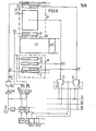
- the transversal filter shown schematically in FIG. 1 is designed as a monolithically integrated semiconductor circuit on a doped semiconductor substrate 1, for example p-type silicon.
- a terminal 2 is supplied with an analog input signal u e , while an analog output signal u a can be tapped at the output 3, the time profile of which corresponds to that of the signal u e after it has passed through a frequency filter with a specific frequency characteristic.
- the frequency characteristic can be that of a low pass, for example.
- a shift register denoted by 4 is designed as a charge-coupled arrangement (CCD) and operates in 3-phase operation. It has a series of electrodes 4 1 1, 412, 413, 422, 423 etc. which are placed close to one another in the direction of displacement R over a thin insulating layer covering the substrate 1, for example a gate oxide layer made of SiO 2 .
- Each three electrodes lying next to each other e.g. 411, 412 and 413 or 42 1 , 422 and 423, belong to a shift register stage, the first electrodes 411, 421 etc. of all stages being connected to a line 5 and connected via this to a shift clock voltage ⁇ 1 while the second electrodes 412, 422 etc. are on a common line 6 connected to a shift clock voltage ⁇ 2 and the third electrodes 413, 423 etc. are connected to a line 7 connected to a shift clock voltage ⁇ 3 .
- each third electrode local maxima of surface potential ⁇ s in the semiconductor substrate 1 So-called potential pots, which are shifted step by step from step to step in the direction of the voltages ⁇ 1 to ⁇ 3 in the direction R. Now one injects electrical charges into these potential pots, each surrounded by space charge zones, which have a polarity that corresponds to that of the minority charge carriers of the substrate 1,
- the output stage AS contains a diffusion region 9 (floating diffusion output) which is temporarily released from external potentials. This is conductively connected to the output 3 via an output amplifier 10.
- the region 9 together with a second diffusion region 11, which is connected via a connection 1 2 to a drain voltage V DD , and a gate electrode 13, which is connected via line 5 to the shift clock voltage ⁇ 1 , represents a field effect transistor which occurs when it occurs of the individual voltage pulses of ⁇ 1 intermittently sets the area 9 to a reference potential.
- the input 2 of the transversal filter is connected to a series of parallel inputs 21, 22, 2n, which are each assigned to individual stages of the shift register 4.
- Leather of these parallel inputs is provided with an evaluation circuit 81, 82, 8n. These each have an area D doped in opposition to the substrate 1 , a first input gate G1, a second input gate G2 and a transfer gate G3, the areas D of all conversion circuits 81 to 8n being formed contiguously and connected to a connection 14, while the transfer gate electrodes G3 all evaluation circuits are also coherent and are provided with a connection 15.
- the first input gate G1 Evaluation circuit 81 is provided with a connection E11, G2 with a connection E12.
- connections E21 and E22 those of the evaluation circuit 8n with En1 and En2.
- the connections E11, E21 and En1 are each connected to the parallel inputs 21, 22 and 2n, while the connections E11 and E21 are connected to a common connection B1 and the connection En2 to a connection B2.
- the evaluation circuit 81 is shown cut along the line II-II.
- the parts already shown in Figure 1 are provided with the same reference numerals.
- the thin insulating layer on which the parts 6 1 , 62, 63 and 411 are placed is denoted by 16.
- the evaluation circuit 81 is set up for a positive evaluation coefficient.
- a constant DC voltage U1 is supplied to the terminal E11 of the first input gate G1 via B1, which is at most as large as the smallest input signal u e to be evaluated, so that a fixed potential threshold W 1 results for the surface potential ⁇ s below G1.
- the input signal u e is fed to the terminal E12 via the parallel input 21, potential values between P 1 (for the maximum signal u e ) and P 0 (for the minimum signal u e ) being obtained below G2.
- an evaluation circuit for example the circuit 8n in FIG. 1, is set up for a negative evaluation coefficient
- the input signal u e is supplied to its first input gate via the connection En1 from a parallel input 2n, while its second input gate is now supplied via a connection En2 and a connection B2 is occupied with a constant DC voltage U2, which is at least as large as the maximum input signal u e to be evaluated and results in a fixed potential value W2 below G2.
- G1 there are potential values P 1 'for the maximum input signal and P C ' for the minimum input signal u e .
- FIG. 4 schematically shows a transversal filter designed according to the invention.
- the shift register 4 can generally consist of one of the known arrangements, known under the term charge transfer devices (CTD, Charge Transfer Device), as described, for example, in the book by Sequin and Tompsett "Charge Transfer Devices” Academic Press, New York , 1975, pages 1 to 18 are described.
- CCD Charge Transfer Device
- Such a charge transfer arrangement can work in 2-phase, 3-phase or 4-phase operation depending on its structure.
- the individual stages of the shift register are shown as blocks in FIG. 4 and are designated 401, 402 to 40n.
- the output stage is again designated AS, while the input stage indicated by 19 in FIG. 1 is omitted because of the better overview.
- the input signal u e supplied via the connection 2 is connected to the parallel inputs 21, 22 to 2n of the shift register 4 and further to the connections E12 and E22 of the evaluation circuits 81 and 82 and to the connection En1 of the evaluation circuits 8n.
- u e is connected to the first input gate G1, while the second input gate G2 is connected to a constant DC voltage U2, which is at least is as large as the largest signal u e . It follows from this that the evaluation circuits 81 and 82 are set up for a positive evaluation coefficient, whereas the circuit 8n is set up for a negative one.
- the evaluation circuits 81, 82 ... 8n are provided with connections 151, 152 ... 15n, to which the clock voltages for the individual transfer gate electrodes G3 are each supplied separately. These clock voltages are derived from a clock voltage Um supplied via a connection TA via a series of AND gates 51, 52 to 5n, the first inputs of which are connected to TA and the outputs of which are connected to connections 151, 152 to 15n. Your second inputs are connected to the outputs of comparators Kol, Ko2 ... Kon. The first inputs of all the comparators Ko1 to Kon are also at the output of a counter Z, the input of which is connected to the terminal TA. The second inputs of the comparators are connected to the outputs of a series of digital memories SP 1 to SPn, the input lines L of which are led to an input K.
- the counter Z Via K and the input line L of the first digital memory SP1, a number in the form of a digital signal is now first entered into it.
- the comparator Ko1 which compares the digital signal stored in SP1 with the output signal of the counter Z, in turn supplies an output signal which opens the AND gate 51 until the counter output signal or the respective counter reading expressed thereby reaches the digital signal in the memory SP1 or exceeds.
- the clock voltage U T is the terminal 151 of the evaluation circuit 81 from the time t 3 of resetting the counter Z via the open AND gate 51 as long as clock voltage ⁇ G '(Fig.
- the number stored in SP1 which can also have several digits, it can thus be precisely determined how often the amount of charge F, which is proportional to the respective amplitude of u e, is read into stage 401 via input 21.
- the repetition frequency of the voltage ⁇ G 'or' U T must be significantly higher than the repetition frequency of the shift clock voltage ⁇ 1 .
- a frequency divider TE the high repetition rate of U T to the ⁇ for the shift clock voltage 1 required value is lowered, wherein discharged via a flip-flop circuit FF, the voltages ⁇ 1 to ⁇ 3 from the divided clock voltage U T.
- the other digital memories SP2 to SPn can be assigned other digital signals, the numerical values entered blocking the inputs 152 to 15n in the same way via the comparators Ko2 to Kon and the AND gates 52 to 5n as soon as the counter reading the single ones Has reached or exceeded numbers.
- the parallel input 2n is connected to the input En2 of the evaluation circuit 8n and En1 is simultaneously supplied with the constant DC voltage U1, the sign of the evaluation coefficient is also positive for the evaluation circuit 8n.
- each of the evaluation circuits 81, 82 or one of the others can also be set up for negative signs by supplying u e to the respective first gate electrode G1 and simultaneously supplying U2 to the gate electrode G2.
- additional parallel inputs 21 ', 22' to 2n ' are provided which, via assigned evaluation circuits 81', 82 'to 8n', enable charge input at the same stages of the shift register 4 as the parallel inputs 21, 22 to 2n, but in each case on the opposite side of the transfer channel of 4.
- the evaluation circuits 81 to 8n are all aligned for a positive evaluation coefficient, while the evaluation circuits 81 'to 8n' are all aligned for a negative one.
- the sign of the individual evaluation coefficients is electrically programmable. This is done by the fact that the evaluation circuit of one, for example 81 ', of two opposing parallel inputs, for example 21 and 21', is permanently blocked at its one clock voltage input, for example 151 ', which can be done by entering the number "0" in the assigned memory, for example SP1 '. This means that only one of the two opposite parallel inputs is effective and determined by its circuitry the sign of the weighting coefficient assigned to the respective shift register level. In this way, the signs of the evaluation coefficients for the individual stages 401, 402 ... 40n can be selected independently of one another.
- the individual digital memories SP1 to SPn and possibly SP1 'to SPn' consist of the stages of a static shift register, in which the stored information does not have to be regenerated. All numbers to be stored are entered in the order of the stages SP1 ', SP2' one after the other via the input K and the input line L.
- FIG. 5 schematically shows another exemplary embodiment of the invention, in which the evaluation circuits 81 and 81 'located on the first stage 401 of the shift register on different sides of the transfer channel with the parts D, G1, G2 already described with reference to FIGS. 1 and 4, and G 3 or D ', G1', G2 'and G3' are provided.
- the first input gate electrodes G1 and G1 ' are led to a common connection E11, the second input gate electrodes G2 and G2' to a common connection E12.
- Both evaluation circuits are thus set up for a positive evaluation coefficient when supplying the input signal u from the parallel input 21 to the terminal E12 and with simultaneous supply of U1 to E11, while they have a negative sign when supplying u e to E11 and simultaneous occupancy E12 with the DC voltage U2 surrender.
- SPV1 and SPV2 which can again be designed as stages of the statistical shift register already described with reference to FIG. 4, are reached.
- the output of SPV 1 is connected to gate electrodes of two field effect transistors T1 and T2, the output of SPV2 to the gate electrodes of two further field effect transistors T3 and T4.
- the source-drain path of T2 is between connection 21 and E11, that of T3 between 21 and E 12, that of T1 between B2 and E12 and that of T4 between B1 and E11.
- T3 and T4 are conductive, which leads to the supply of u e to El2 and the supply of U1 on E11 means.
- the circuit 81 is thus designed for a positive evaluation coefficient, which also applies to the circuit 81 '. If a "1" is stored in SPV1, but a "0" in SPV2, u e is connected to connection E11 and U2 to connection E12. A negative sign of the evaluation coefficients of the circuits 81 and 81 'is thus achieved.
- the supply of the clock voltages ⁇ G 'and ⁇ G "provided for the transfer gate electrodes G3 of the circuits 81 and 81' at the inputs 151 and 151 ' is carried out in the manner already described with reference to FIG. 4 via AND gates 51 and 51', comparators Ko1 and Kol ', digital memories SP1 and SP1' and a counter Z controls, the counter Z and the first inputs of the AND gates 51 and 51 'are again connected to a terminal TA, at which a clock voltage U T is obtained. From the voltage U T is also used to derive the clock voltage ⁇ D 'supplied to the regions D and D' doped opposite to the substrate via an inverter INV1 and a delay element VZ.
- the amounts of charge read in via 81 'and 81 are in the ratio of the areas of G2' and G2, this ratio preferably being able to assume a value of 10 or 100.
- the number of the amounts of charge read in is determined by the digital numbers stored in S P 1 and SP1 '. The combination of both read-in processes results in a very fast read-in, even with coefficients whose amount is determined by large digital numerical values.
- the exemplary embodiment of the invention shown in FIG. 6 differs from FIG. 5 only in that the common connections E11 and E12 are actuated differently.
- the evaluation circuits 81 and 81 'for a positive evaluation coefficient which is done by supplying u to E12 and U1 to E11, a "1" is stored in SPV1 and a "0" in SPV2, one via the output of SPV1 controlled switching transistor T5 opens and connects the parallel input 21 to the terminal E12.
- a negative coefficient is set if a "0" is stored in SPV1 and a "1" in SPV2.
- a switching transistor T6 controlled via the output of SPV2 opens, the source-drain path of which is connected on the one hand via an inverter In to 21 and on the other hand to E12.
- the inverted input signal u is thus supplied to the terminal E12, while E 11 is assigned U1.
Abstract
Transversalfilter das ein CTD-Schieberegister (4) verwendet mit Paralleleingängen (2) und diesen zugeordneten Bewertungsschaltungen (81, 82, 83), die durch Mehrfach-Einlesen von signalabhängigen Ladungsmengen Bewertungskoeffizienten bilden. Die im Schieberegister (4) aufsummierten und nacheinander die Ausgangsstufe (AS) erreichenden Ladungen werden zur Bildung des gefilterten Ausgangssignals seriell ausgelesen. Es wird eine elektrische Koeffizienteneinstellung angestrebt, die bei einem geringen Bedarf an Halbleiterfläche einen grossen relativen Einstellbereich gewährleistet. Hierzu sind Bewertungsschaltungen (81, 82) vorgesehen deren Taktspannungen über Torschaltungen (51,52) gesteuert werden. Die Steuerung erfolgt in Abhängigkeit von einem digitalen Vergleich zwischen dem Ausgangssignal eines die Taktspannungsimpulse zählenden Zählers (Z) und Signalen, die in digitale Speicher (SP1, SP2) eingegeben und den Bewertungsschaltungen (81, 82) individuell zugeordnet sind. Die digitalen Speicher (SP1, SP2) werden vorzugsweise durch die Stufen eines statischen Schieberegisters gebildet. Das Transversalfilter ist für den Einsatz als elektrisch programmierbares Frequenzfilter geeignet.Transversal filter that uses a CTD shift register (4) with parallel inputs (2) and associated evaluation circuits (81, 82, 83), which form evaluation coefficients by multiple reading of signal-dependent charge quantities. The charges added up in the shift register (4) and successively reaching the output stage (AS) are read out serially to form the filtered output signal. An electrical coefficient setting is sought, which ensures a large relative setting range with a small need for semiconductor area. For this purpose, evaluation circuits (81, 82) are provided, the clock voltages of which are controlled via gate circuits (51, 52). Control takes place as a function of a digital comparison between the output signal of a counter (Z) counting the clock voltage pulses and signals which are input into digital memories (SP1, SP2) and individually assigned to the evaluation circuits (81, 82). The digital memories (SP1, SP2) are preferably formed by the stages of a static shift register. The transversal filter is suitable for use as an electrically programmable frequency filter.
Description
Die Erfindung bezieht sich auf ein Transversalfilter, bei dem die Stufen eines auf einem dotierten Halbleitersubstrat integrierten, analogen CTD-Schieberegisters mit Paralleleingängen und diesen zugeordneten Bewertungsschaltungen versehen sind, bei dem die Bewertungsschaltungen jeweils ein entgegengesetzt zu dem Substrat dotiertes Gebiet, ein erstes und zweites Eingangsgate und ein Transfergate aufweisen, wobei das Transfergate unmittelbar neben dem Transferkanal des CTD-Schieberegisters angeordnet ist, das eine Eingangsgate mit einem Eingangssignal, das andere Eingangsgate mit einer konstanten Gleichspannung, das entgegengesetzt dotierte Gebiet mit einer ersten und das Transfergate mit einer zweiten Taktspannung beschaltet sind, und bei dem das Ausgangssignal an einem Ausgang des CTD-Schieberegisters abgreifbar ist.The invention relates to a transversal filter, in which the stages of an analog CTD shift register integrated on a doped semiconductor substrate are provided with parallel inputs and evaluation circuits associated therewith, in which the evaluation circuits each have a region doped opposite to the substrate, a first and a second input gate and have a transfer gate, the transfer gate being arranged directly next to the transfer channel of the CTD shift register, the one input gate having an input signal, the other input gate having a constant DC voltage, the oppositely doped region being connected to a first and the transfer gate having a second clock voltage , and in which the output signal can be tapped at an output of the CTD shift register.
Ein derartiges Transversalfilter ist aus der Zeitschrift "Electronics Letters", Bd. 13, Nr. 5 vom 3. März 1977, Seiten 126 und 127, bekannt. Die Größe der einzelnen Koeffizienten, mit denen das Eingangssignal an jedem Paralleleingang individuell bewertet wird, ist dabei durch die Kapazität des zweiten Eingangsgate gegeben. Transversalfilter dieser Gattung bilden auch den Gegenstand der deutschen Patentanmeldung P 26 43 704.7.Such a transversal filter is from the magazine "Electronics Letters", Vol. 13, No. 5 dated March 3, 1977, Pages 126 and 127, known. The size of the individual coefficients with which the input signal is individually evaluated at each parallel input is given by the capacitance of the second input gate. Transversal filters of this type also form the subject of the German patent application P 26 43 704.7.
Aus den "Proceedings of the 8th Conference (1976 International) on Solid State Devices, Tokyo, 1976", abgedruckt im "Japanese Journal of Applied Physics", Vol. 16 (1977) Supplement 16-1, Seiten 387-390 ist ein solches Transversalfilter bekannt, bei dem ein CCD-Schieberegister mehrere durch Trenndiffusionen gegeneinander isolierte Transferkanäle aufweist, die den Paralleleingängen jeweils individuell zugeordnet sind. Hierbei besteht das in den Bewertungsschaltungen jeweils vorgesehene Transfergate aus der ersten Verschiebeelektrode des zugehörigen Transferkanals. Die Transferkanäle werden in einer gemeinsamen Ausgangsstufe, in deren Bereich die genannten Trenndiffusionen weggelassen sind, zusammengeführt. Dort erfolgt eine Summierung der über die Kanäle getrennt übertragenen und mit unterschiedlichen Verzögerungen eintreffenden Signalanteile zu einem Ausgangssignal. Die Bewertungskoeffizienten, mit denen das den Paralleleingängen zugeführte Signal belegt wird, sind durch die Gateflächen in den einzelnen Bewertungsschaltungen gegeben. Nachteilig ist hierbei, daß die erforderliche Halbleiterfläche mit der Anzahl der Paralleleingänge stark ansteigt.One such is from the "Proceedings of the 8th Conference (1976 International) on Solid State Devices, Tokyo, 1976", printed in the "Japanese Journal of Applied Physics", vol. 16 (1977) Supplement 16-1, pages 387-390 Transverse filter is known, in which a CCD shift register has a plurality of transfer channels isolated from one another by separating diffusions, each of which is individually assigned to the parallel inputs. In this case, the transfer gate provided in the evaluation circuits consists of the first displacement electrode of the associated transfer channel. The transfer channels are brought together in a common output stage, in the area of which the above-mentioned separation diffusions have been omitted. There, the signal components transmitted separately via the channels and arriving with different delays are summed to form an output signal. The weighting coefficients with which the signal fed to the parallel inputs is occupied are given by the gate areas in the individual weighting circuits. The disadvantage here is that the required semiconductor area increases sharply with the number of parallel inputs.
Aus den oben genannten "Proceedings", abgedruckt in dem "Japanese Journal of Applied Fhysics", Vol. 16 (1977), Supplement 16-1, Seiten 391-396, ist ein weiteres Transversalfilter bekannt, das sich von der eingangs erwähnten Gattung durch eine andere Ausbildung der Bewertungsschaltungen und der Paralleleingänge unterscheidet. Jede einzelne Bewertungsschaltung enthält hier zwei in Serie geschaltete MOS-Feldeffekttransistoren und eine Widerstandsdiffusion, während jeder Paralleleingang eine mit einer Eingangsdiffusion versehene Stufe eines Vier-Phasen-CCD-Schieberegisters aufweist. Dabei ist die Eingangsdiffusion mit einem Anschluß des Widerstandes verbunden und die letzte Verschiebeelektrode zu einer Verschiebeelektrode eines die Summierung der Signalanteile vornehmenden CCD-Schieberegisters benachbart angeordnet. Das Gate des einen MOS-Feldeffekttransistors jeder Bewertungsschaltung wird mit dem Eingangssignal belegt, das Gate des anderen jeweils mit einer Gleichspannung, di.e durch ihre Größe den durch die Transistoren fließenden Strom und damit den jeweiligen Bewertungskoeffizienten bestimmt. Damit sind die Übertragungseigenschaften des Transversalfilters elektrisch einstellbar. Nachteilig ist jedoch, daß der Strom nur in einem kleinen Änderungsbereich linear von der genannten Gleichspannung abhängt.A further transversal filter is known from the "Proceedings" mentioned above, printed in the "Japanese Journal of Applied Physics", Vol. 16 (1977), Supplement 16-1, pages 391-396, which differs from the type mentioned at the outset another education of the Be differentiating circuits and the parallel inputs. Each individual evaluation circuit here contains two MOS field-effect transistors connected in series and a resistance diffusion, while each parallel input has a stage of a four-phase CCD shift register provided with an input diffusion. The input diffusion is connected to a connection of the resistor and the last shift electrode is arranged adjacent to a shift electrode of a CCD shift register which makes the summation of the signal components. The gate of the one MOS field-effect transistor of each evaluation circuit is assigned the input signal, the gate of the other is in each case determined by a DC voltage, ie the size of the current flowing through the transistors and thus the respective evaluation coefficient. The transmission properties of the transversal filter can thus be set electrically. It is disadvantageous, however, that the current depends linearly on the DC voltage mentioned only in a small change range.
Es wurde bereits vorgeschlagen, vergl. die ältere deutsche Patentanmeldung P 26 44 284.2, bei einem Transversalfilter der eingangs genannten Art in den einzelnen Bewertungsschaltungen zur Realisierung eines Bewertungskoeffizienten jeweils zweimal hintereinander Ladungsmengen zu bilden und in die zugehörigen Stufen des CTD-Schieberegisters einzugeben, um die Bewertungsschaltungen flächensparend ausbilden zu können.It has already been proposed to compare the older German patent application P 26 44 284.2 with a transversal filter of the type mentioned in the individual evaluation circuits for realizing an evaluation coefficient twice in succession to form charge quantities and to enter them in the associated stages of the CTD shift register in order to enter the To be able to train evaluation circuits to save space.
Der vorliegenden Erfindung liegt die Aufgabe zugrunde, ein Transversälfilter der eingangs genannten Art vorzusehen, dessen Bewertungskoeffizienten mit großer Genauigkeit elektrisch einstellbar sind, wobei ein großer relativer Einstellbereich überstrichen werden soll. Das wird gemäß der Erfindung durch die im kennzeichnenden Teil des Patent- anspruches 1-angeführten Maßnahmen erreicht.The present invention is based on the object of providing a transversal filter of the type mentioned at the outset, the weighting coefficients of which can be set electrically with great accuracy, a large relative setting range being to be covered. This is according to the invention by the in the characterizing part of the patent Claim 1-listed measures achieved.
Der mit der Erfindung erzielte Vorteil besteht insbesondere darin, daß durch die gespeicherten digitalen Signale in sehr übersichtlicher Weise festgelegt ist, wie oft aus einer Bewertungsschaltung eine durch deren Fläche gegebene Ladungsmenge in die zugehörige Stufe des CTD-Schieberegisters eingegeben wird, wobei sich aus der Anzahl der jeweils eingegebenen Ladungsmengen die den Bewertungsschaltungen zugeordneten Bewertungskoeffizienten ergeben. Da das Eingeben der Ladungsmengen mit einer wesentlich höheren Frequenz erfolgen kann als das Takten des CTD-Schieberegistsrs, ist es möglich, für die Bewertungskoeffizienten große relative Einstellbereiche vorzusehen, die beispielsweise Größenverhältnisse von 1:1000 oder mehr einschließen. Zwischen der die Einstellung eines Bewertungskoeffizienten kontrollierenden Größe, das heißt dem eingespeicherten digitalen Signal, und dem eingestellten Bewertungskoeffizienten besteht dabei eine linieare Abhängigkeit. Die einfache und innerhalb weiter Grenzen gegebene Einstellbarkeit der Bewertungskoeffizienten ermöglicht eine sehr vielseitige Anwendung des erfindungsgemäßen Transversalfilters.The advantage achieved by the invention is, in particular, that the stored digital signals determine in a very clear manner how often an amount of charge given by its area is entered into the associated stage of the CTD shift register from an evaluation circuit, the number depending on the number of the respectively entered quantities of charge result in the evaluation coefficients assigned to the evaluation circuits. Since the charge quantities can be input at a significantly higher frequency than the clocking of the CTD shift register, it is possible to provide large relative setting ranges for the evaluation coefficients, which include, for example, size ratios of 1: 1000 or more. There is a linear dependency between the quantity controlling the setting of an evaluation coefficient, that is to say the stored digital signal, and the set evaluation coefficient. The simple adjustability of the evaluation coefficients, which is provided within wide limits, enables the transversal filter according to the invention to be used in a very versatile manner.
Die Erfindung wird nachfolgend anhand einiger in der Zeichnung dargestellter, bevorzugter Ausführungsbeispiele näher erläutert.The invention is explained in more detail below with reference to some preferred exemplary embodiments shown in the drawing.
Dabei zeigt:
- Fig. 1 eine Prinzipdarstellung des eingangs erwähnten, bekannten Transversalfilters mit einem CCD-Schieberegister mit Paralleleingängen und einem Serienausgang,
- Fig. 2 einen Querschnitt durch eine Teilschaltung von Fig. 1,
- Fig. 3 ein Zeitdiagramm der für ein Transversalfilter nach den
Figuren 1 und 2 erforderlichen Betriebsspannungen, - Fig. 4 ein erstes Ausführungsbeispiel der Erfindung,
- Fig. 5 ein zweites Ausführungsbeispiel und
- Fig. 6 ein weiteres Ausführungsbeispiel der Erfindung.
- 1 is a schematic diagram of the known transversal filter mentioned at the outset with a CCD shift register with parallel inputs and a series output,
- 2 shows a cross section through a subcircuit of FIG. 1,
- 3 shows a time diagram of the operating voltages required for a transversal filter according to FIGS. 1 and 2,
- 4 shows a first embodiment of the invention,
- Fig. 5 shows a second embodiment and
- Fig. 6 shows another embodiment of the invention.
Das in Figur 1 schematisch dargestellte Transversalfilter ist als eine auf einem dotierten Halbleitersubstrat 1, z.B. p-leitendem Silizium, monolithisch integrierte Halbleiterschaltung ausgebildet. Einem Anschluß 2 wird ein analoges Eingangssignal ue zugeführt, während am Ausgang 3 ein analoges Ausgangssignal ua abgreifbar ist, dessen zeitlicher Verlauf dem des Signals ue entspricht, nachdem dieses ein Frequenzfilter mit einer bestimmten Frequenzcharakteristik durchlaufen hat. Die Frequenzcharakteristik kann beispielsweise die eines Tiefpasses sein. Ein mit 4 bezeichnetes Schieberegister ist als eine ladungsgekoppelte Anordnung (CCD) ausgebildet und arbeitet im 3-Fhasen-Betrieb. Sie weist eine Reihe von Elektroden 411, 412, 413, 422, 423 usw. auf, die über einer das Substrat 1 abdeckenden, dünnen Isolierschicht, z.B. einer Gateoxidschicht aus Si02, dicht nebeneinanderliegend in Verschieberichtung R plaziert sind.The transversal filter shown schematically in FIG. 1 is designed as a monolithically integrated semiconductor circuit on a
Jeweils drei nebeneinander liegende Elektroden, z.B. 411, 412 und 413 oder 421, 422 und 423, gehören zu einer Schieberegisterstufe, wobei die ersten Elektroden 411, 421 usw. sämtlicher Stufen an eine Leitung 5 angeschlossen und über diese mit einer Verschiebetaktspannung φ1 beschaltet sind, während die zweiten Elektroden 412, 422 usw. an einer gemeinsamen, mit einer Verschiebetaktspannung φ2 beschalteten Leitung 6 und die dritten Elektroden 413, 423 usw. an einer mit einer Verschiebetaktspannung φ3 beschalteten Leitung 7 liegen. Bei einem zeitlichen Verlauf der Spannungen φ1 bis φ3 gemäß Figur 3 ergeben sich unterhalb jeder dritten Elektrode lokale Maxima des Oberflächenpotentials φs im Halbleitersubstrat 1, sogenannte Potentialtöpfe, die im Takte der Spannungen φ1 bis φ3 in Richtung R schrittweise von Stufe zu Stufe verschoben werden. Injiziert man nun in diese jeweils von Raumladungszonen umgebenen Potentialtöpfe elektrische Ladungen, die eine Polarität aufweisen, die der der Minoritätsladungsträger des Substrates 1 entspricht,Each three electrodes lying next to each other, e.g. 411, 412 and 413 or 42 1 , 422 and 423, belong to a shift register stage, the first electrodes 411, 421 etc. of all stages being connected to a line 5 and connected via this to a shift clock voltage φ 1 while the second electrodes 412, 422 etc. are on a common line 6 connected to a shift clock voltage φ 2 and the third electrodes 413, 423 etc. are connected to a line 7 connected to a shift clock voltage φ 3 . At a time profile of the voltages φ 1 to φ 3 according to Figure 3 will become apparent below each third electrode local maxima of surface potential φ s in the semiconductor substrate 1, So-called potential pots, which are shifted step by step from step to step in the direction of the voltages φ 1 to φ 3 in the direction R. Now one injects electrical charges into these potential pots, each surrounded by space charge zones, which have a polarity that corresponds to that of the minority charge carriers of the
so werden diese mit den Potentialtöpfen verschoben und können nach dem Durchlaufen des gesamten Schieberegisters 4 in dessen Ausgangsstufe AS zeitverzögert ausgelesen werden. Bei der in Figur 1 dargestellten Ausführungsform des Schieberegisters 4 enthält die Ausgangsstufe AS ein zeitweilig von äußeren Potentialen freigeschaltetes Diffusionsgebiet 9 (floating diffusion output). Dieses ist über einen Ausgangsverstärker 10 mit dem Ausgang 3 leitend verbunden. Das Gebiet 9 stellt zusammen mit-einem zweiten Diffusionsgebiet 11, das über einen Anschluß 12 mit einer Drainspannung VDD beschaltet ist, und einer Gateelektrode 13, die über die Leitung 5 an ier Verschiebetaktspannung φ1 liegt, einen Feldeffekttransistor dar, der beim Auftreten der einzelnen spannungsimpulse von φ1 das Gebiet 9 intermittierend auf ein Referenzpotential setzt.so they are shifted with the potential wells and can be read out after the
Der Eingang 2 des Transversalfilters ist mit einer Reihe von Paralleleingängen 21, 22, 2n verbunden, die jeweils einzelnen Stufen des Schieberegisters 4 zugeordnet sind. leder dieser Paralleleingänge ist mit einer Bewertungsschaltung 81, 82, 8n versehen. Diese weisen jeweils ein entgegengesetzt zum Substrat 1 dotiertes Gebiet D, ein erstes Eingangsgate G1, ein zweites Eingangsgate G2 und ein Transfergate G3 auf, wobei die Gebiete D aller Bevertungsschaltungen 81 bis 8n zusammenhängend ausgebildet und mit einem Anschluß 14 verbunden sind, während die Transfergateelektroden G3 aller Bewertungsschaltungen ebenfalls zusammenhängend ausgebildet und mit einem Anschluß 15 versehen sind. Das erste Eingangsgate G1 der Bewertungsschaltung 81 ist mit einem Anschluß E11 versehen, G2 mit einem Anschluß E12. Die entsprechenden Anschlüsse von 82 sind mit E21 und E22 bezeichnet, die der BewertungsschaLtung 8n mit En1 und En2. In Figur 1 sind die Anschlüsse E11, E21 und En1 jeweils mit den Paralleleingängen 21, 22 und 2n verbunden, während die Anschlüsse E11 und E21 an einen gemeinsamen Anschluß B1 und der Anschluß En2 an einen Anschluß B2 geführt sind.The input 2 of the transversal filter is connected to a series of
In Figur 2 ist die Bewertungsschaltung 81 längs der Linie II-II geschnitten dargestellte Dabei sind die bereits in Figur 1 gezeigten Teile mit denselben Bezugszeichen versehen. Die dünne Isolierschicht, auf der die Teile 61, 62, 63 und 411 plaziert sind, ist mit 16 bezeichnet. Die Bewertungsschaltung 81 ist für einen positiven Bewertungskoeffizienten eingerichtet. Dabei wird dem Anschluß E11 des ersten Eingangsgate G1 über B1 eine konstante Gleichspannung U1 zugeführt, die höchstens so groß ist wie das kleinste zu bewertende Eingangssignal ue, so daß sich für das Oberflächenpotential φs unterhalb von G1 eine feste Potentialschwelle W1 ergibt. Dem Anschluß E12 wird über den Paralleleingang 21 das Eingangssignal ue zugeführt, wobei sich unterhalb von G2 Potentialwerte zwischen P1 (für das maximale Signal üe) und P0 (für das minimale Signal ue) ergeben.In Figure 2, the
Unter dem Einfluß der in Figur 3 dargestellten Taktspannungen φG und φD, die jeweils den Anschlüssen 14 und 15 zugeführt werden, ergeben sich Potentialwerte D1 bzw. D0 und T1 bzw. TO innerhalb des dotierten Gebietes D und unterhalb des Transfergate G3 gemäß Figur 2. Zum Zeitpunkt tO (Fig. 3) besteht ein Potentialverlauf DO, W1' P, T0 und CO, wobei der Potentialwert P durch die Größe des auftretenden Eingangssignales ue gegeben ist. Dabei wird der unterhalt von G2 gebildete Potentialtopf mit Ladungsträgern überschwemmt. Zum Zeitpunkt t1 ist DO in D1 übergegangen, wobei die Ladungsträger wieder soweit aus dem Bereich unterhalb von G1 und G2 in das Gebiet D zurückfließen, daß der unterhalb von G2 gebildete Potentialtopf nur noch bis zu dem durch W1 gegebenen Rand angefüllt bleibt, was in Figur 2 durch die schraffierte Fläche F angedeutet ist. Ist dann TO in T1 übergegangen (Zeitpunkt t2) so wird die durch F angedeutete Ladungsmenge entsprechend dem Pfeil 17 unter die Elektrode 411 verschoben, da diese gleichzeitig mit einer relativ hohen Verschiebetaktspannung φ1 belegt ist, die einen Potentialwert C1 ergibt. Wesentlich ist hierbei, daß bei einer Ausbildung der Schaltung 81 für einen positiven Bewertungskoeffizienten beim Auftreten des minimalen Eingangssignais ue wegen P=PO keine Ladungsmenge eingelesen wird, beim Auftreten des maximalen Eingangssignals ue wegen P=P1 die maximale Ladungsmenge, die durch die zwischen den Werten Po und P1 liegende Fläche dargestellt werden kann. Der Einlesevorgang wiederholt sich mit der Frequenz der Verschiebe- taktspannung φ1.Under the influence of the clock voltages φ G and φ D shown in FIG. 3, which are respectively fed to the
Ist eine Bewertungsschaltung, z.B. die Schaltung 8n in Figur 1, für einen negativen Bewertungskoeffizienten eingerichtet, so wird ihrem ersten Eingangsgate über den Anschluß En1 von einem Paralleleingang 2n das Eingangssignal u e zugeführt, während ihr zweites Eingangsgate über einen Anschluß En2 und einen Anschluß B2 nunmehr mit einer konstanten Gleichspannung U2 belegt ist, die wenigstens so groß ist wie das maximale zu bewertende Eingangssignal ue und unterhalb von G2 einen festen Potentialwert W2 ergibt. Unterhalb von G1 ergeben sich dann Potentialwerte P1' für das maximale Eingangssignal und PC' für das minimale Eingangssignal ue. Das Anfüllen des Potentialtopfes unterhalb von G2 ist dabei nur bis zu dem durch das zum Zeitpunkt t1 anliegende Eingangssignal ue bestimmten Rand P' möglich, was in Figur 2 durch die Fläche F' gekennzeichnet ist. Nach dem Übergang von TO auf T1 und von Co auf C1 (Zeitpunkt t2) wird die Ladungsmenge F' wieder unter eine Elektrode des CCD-Schieberegisters 4 verschoben (Pfeil 8). Wesentlich ist, daß bei einem negativen Bewertungskoeffizienten beim Auftreten des minimalen Eingangssignals ue wegen P'=PO' die maximale Ladungsmenge eingegeben wird, was in Figur 2 durch eine Fläche unterhalb von G2 und zwischen den Potentialwerten PO' und P1' verdeutlicht wird, während für das maximale Eingangssignal ue wegen P'=P1' keine Ladungsmenge eingelesen wird. Auch dieser Einlesevorgang wiederholt sich mit der Frequenz der Verschiebetaktspannung φ1.If an evaluation circuit, for example the
Somit finden in dem Schieberegister 4 unter den Elektroden 411, 421 usw. jeweils beim Auftreten der Verschiebetaktspannungen φ1 Summierungsvorgänge statt, bei denen zu den jeweils innerhalb des Schieberegisters 4 verschobenen Ladungsmengen die über die zugehörigen Paralleleingänge eingegebenen Ladungsmengen F bzw. F' addiert werden. Die auf diese Weise durch mehrfache Summierungsvorgänge angewachsenen Ladungsmengen, die schließlich in der letzten Stufe des Schieberegisters 4 nacheinander ankommen, bewirken dann beim Eindringen in das Diffusionsgebiet 9, das zuvor auf Referenzpotential gebracht wurde, jeweils Potentialverschiebungen, die über den Verstärker 10 ausgewertet und zu dem gefilterten Ausgangssignal ua zusammengesetzt werden.Thus, in the
Man kann durch eine mit 19 angedeutete, an sich bekannte Eingangsstufe des Schieberegisters 4, die beispielsweise in dam Buch von Sequin und Tompsett "Charge Transfer Devi:es'', Academic Press, New York, 1975 auf den Seiten 48 bis 50, insbesondere Figur 3.12(d), beschrieben ist, zu den äber das Schieberegister verschobenen Ladungsmengen eine konstante Grundladung hinzufügen, die in der Literatur auch als "fat zero" bezeichnet wird. Hierbei besteht das dieser Eingangsstufe zugeführte Signal aus einer Gleichspannung.An input stage of the
In Figur 4 ist ein nach der Erfindung ausgebildetes Transversalfilter schematisch dargestellt. Dabei sind die bereits anhand der Figuren 1 bis 3 beschriebenen Teile mit den gleichen Bezugszeichen versehen. Das Schieberegister 4 kann jedoch ganz allgemein aus einer .der unter dem Begriff Ladungsverschiebeanordnungen (CTD, Charge Transfer Device) zusammengefaßten, an sich bekannten Anordnungen bestehen, wie sie beispielsweise in dem Buch von Sequin und Tompsett "Charge Transfer Devices" Academic Press, New York, 1975, Seiten 1 bis 18 beschrieben sind. Eine solche Ladungsverschiebeanordnung kann dabei entsprechend ihrem Aufbau im 2-Phasen-, 3-Phasen- oder 4-Phasen-Betrieb arbeiten. Die einzelnen Stufen des Schieberegisters sind in Figur 4 als Blöcke dargestellt und mit 401, 402 bis 40n bezeichnet. Die Ausgangsstufe ist wieder mit AS bezeichnet, während die in Figur 1 mit 19 angedeutete Eingang sstufe wegen der besseren Übersicht weggelassen ist. Das über den Anschluß 2 zugeführte Eingangssignal ue liegt an den Paralleleingängen 21, 22 bis 2n des Schieberegisters 4 und weiter an den Anschlüssen E12 und E22 der Bewertungsschaltungen 81 und 82 sowie an den Anschluß En1 der Bewertungsschaltungen 8n. Damit ist ue jeweils an das zweite Eingangsgate G2 der Schaltungen 81 und 82 geführt, während jeweils das erste Eingangsgate G1 dieser Schaltungen mit einer konstanten Gleichspannung U1 beschaltet sind, die höchstens so groß ist wie das kleinste Signal ue.. Bei der Bewertungsschaltung 8n ist ue an das erste Eingangsgate G1 geführt, während das zweite Eingangsgate G2 an einer konstanten Gleichspannung U2 liegt, die wenigstens so groß ist wie das größte Signal ue. Hieraus ergibt sich, daß die Bewertungsschaltungen 81 und 82 für einen positiven Bewertungskoeffizienten eingerichtet sind, die Schaltung 8n dagegen für einen negativen.FIG. 4 schematically shows a transversal filter designed according to the invention. The parts already described with reference to FIGS. 1 to 3 are provided with the same reference symbols. However, the
Die Bewertungsschaltungen 81, 82 ... 8n sind mit Anschlüssen 151, 152 ... 15n versehen, denen die Taktspannungen für die einzelnen Transfergateelektroden G3 jeweils getrennt zugeführt werden. Dabei sind diese Taktspannungen von einer über einen Anschluß TA zugeführten Taktspannung Um jeweils über eine Reihe von UND-Gattern 51, 52 bis 5n abgeleitet, deren erste Eingänge jeweils mit TA und deren Ausgänge mit den Anschlüssen 151, 152 bis 15n verbunden sind. Ihre zweiten Eingänge sind mit den Ausgängen von Komparatoren Kol, Ko2 ... Kon beschaltet. Die ersten Eingänge aller Komparatoren Ko1 bis Kon liegen ferner am Ausgang eines Zählers Z, dessen Eingang mit dem Anschluß TA verbunden ist. Die zweiten Eingänge der Komparatoren sind-mit den Ausgängen einer Reihe von digitalen Speichern SP1 bis SPn beschaltet, deren Eingabeleitungen L an einen Eingang K geführt sind.The
Über K und die Eingabeleitung L des ersten digitalen Speichers SP1 wird nun in diesen zunächst eine Zahl in Form eines digitalen Signals eingegeben. Nach dem Rücksetzen des Zählers Z beginnt dieser die Impulse der bei TA anliegenden Taktspannung UT zu zählen. Der Komparator Ko1, der das in SP1 gespeicherte digitale Signal mit dem Ausgangssignal des Zählers Z vergleicht, liefert seinerseits nur solange ein das UND-Gatter 51 öffnendes Ausgangssignal, bis das Zählerausgangssignal bzw. der hierdurch ausgedrückte jeweilige Zählerstand das digitale Signal im Speicher SP1 erreicht oder übersteigt. Somit wird die Taktspannung UT dem Anschluß 151 der Bewertungsschaltung 81 vom Zeitpunkt t3 des Rücksetzens des Zählers Z über das geöffnete UND-Gatter 51 solange als Takt- spannung φG' (Fig. 3) zugeführt, bis zum Zeitpunkt t4 die in SP gespeicherte Zahl, im dargestellten Fall die Zahl 3, durch das Zählergebnis erreicht bzw. überschritten wird. Von dem Zeitpunkt t4 an ist die UND-Schaltung 51-dann gesperrt. Für jeden Impuls von φG' wird zwischen den Zeitpunkten t3 und t4 beim Zuführen einer weiteren Taktspannung φD' an das entgegengesetzt dotierte Gebiet D von 81, die aus der Taktspannung φG' über einen Inverter und ein Verzögerungsglied abgeleitet ist, eine bestimmte Ladungsmenge F (Fig. 2) unterhalb von G2 gebildet und entsprechend dem Pfeil 17 jeweils unter eine Verschiebeelektrode der Stufe 401 verschoben. Aus der Anzahl der im Intervall t3 bis t4 eingelesenen Ladungsmengen F ergibt sich dann der Betrag des dem Paralleleingang 21 zugeordneten Bewergungskoeffizienten, aus der Ansteuerung der Bewertungsschaltung 81 sein Vorzeichen. Durch.Wahl der in SP1 gespeicherten Zahl, die auch mehrstellig sein kann, läßt sich somit genau festlegen, wie oft die Ladungsmenge F, die der jeweils anliegenden Amplitude von ue proprotional ist, über den Eingang 21 in die Stufe 401 eingelesen wird. Die Folgefrequenz der Spannung φG' bzw. von'UT muß dazu allerdings wesentlich höher liegen als die Folgefrequenz der Verschiebetaktspannung φ1. Durch einen Frequenzteiler TE wird die hohe Folgefrequenz von UT auf den für die Verschiebetaktspannung φ1 benötigten Wert herabgesetzt, wobei über eine Flip-Flop-Schaltung FF die Spannungen φ1 bis φ3 aus der geteilten Taktspannung UT abgeleitet werden.Via K and the input line L of the first digital memory SP1, a number in the form of a digital signal is now first entered into it. After the counter Z has been reset, it starts counting the pulses of the clock voltage U T present at TA. The comparator Ko1, which compares the digital signal stored in SP1 with the output signal of the counter Z, in turn supplies an output signal which opens the AND
Unabhängig voneinander können die weiteren digitalen Speicher SP2 bis SPn mit anderen digitalen Signalen belegt werden, wobei die eingegebenen Zahlenwerte in gleicher Weise eine Sperrung der Eingänge 152 bis 15n über die Komparatoren Ko2 bis Kon und die UND-Gatter 52 bis 5n vornehmen, sobald der Zählerstand die einzelnen Zahlen jeweils erreicht oder überschritten hat. Führt man beispielsweise den Paralleleingang 2n an den Eingang En2 der Bewertungsschaltung 8n und belegt En1 gleichzeitig mit der konstanten Gleichspannung U1, so ist auch für die Bewertungsschaltung 8n das Vorzeichen des Bewertungskoeffizienten positiv. Andererseits kann auch jede der Bewertungsschaltungen 81, 82 oder eine der weiteren durch Zuführung von ue an die jeweils erste Gateelektrode G1 und gleichzeitige Zuführung von U2 an die Gateelektrode G2 für negative Vorzeichen eingerichtet werden.Independently of one another, the other digital memories SP2 to SPn can be assigned other digital signals, the numerical values entered blocking the
Nach einer Weiterbildung der Erfindung sind zusätzliche Paralleleingänge 21', 22' bis 2n' vorgesehen, die über zugeordnete Bewertungsschaltungen 81', 82' bis 8n' eine Ladungseingabe bei denselben Stufen des Schieberegisters 4 ermöglichen wie die Paralleleingänge 21, 22 bis 2n, aber jeweils auf der gegenüberliegenden Seite des Transferkanals von 4. Dabei müssen zwei einander gegenüberliegende Eingänge, z.B. 21 und 21', jeweils Bewertungsschaltungen, z.B. 81 und 81', aufweisen, die für dasselbe Vorzeichen eingerichtet sind.According to a further development of the invention, additional parallel inputs 21 ', 22' to 2n 'are provided which, via assigned evaluation circuits 81', 82 'to 8n', enable charge input at the same stages of the
Eins andere Weiterbildung der Erfindung sieht vor, daß die Bewertungsschaltungen 81 bis 8n alle für einen positiven Bewertungskoeffizienten ausgerichtet sind, die Bewertungsschaltungen 81' bis 8n' dagegen alle für einen negativen. In diesem Fall ist das Vorzeichen der einzelnen Bewertungskoeffizienten elektrisch programmierbar. Das geschieht dadurch, daß von jeweils zwei einander gegenüberliegenden Paralleleingängen, z.B. 21 und 21', die Bewertungsschaltung des einen, z.B. 81', an ihrem einen Taktspannungseingang, z.B. 151', ständig gesperrt ist, was man durch die Eingabe der Zahl "0" in-den zugeordneten Speicher, z.B. SP1', erreicht. Damit ist von den beiden einander gegenüberliegenden Paralleleingängen nur einer wirksam und bestimmt durch seine Schaltungsgegebenheiten das Vorzeichen des der jeweiligen Schieberegisterstufe zugeordneten Bewertungskoeffizienten. In dieser Weise sind die Vorzeichen der Bewertungskoeffizienten für die einzelnen Stufen 401, 402 ... 40n unabhängig voneinander wählbar.Another development of the invention provides that the
Nach einer bevorzugten Weiterbildung des Erfindungsgedankens bestehen die einzelnen digitalen Speicher SP1 bis SPn und gegebenenfalls SP1' bis SPn' aus den Stufen eines statischen Schieberegisters, bei dem die gespeicherte Information nicht regeneriert werden muß. Dabei erfolgt die Eingabe aller zu speichernden Zahlen in der Reihenfolge der Stufen SP1', SP2' nacheinander über den Eingang K und die Eingabeleitung L.According to a preferred development of the inventive concept, the individual digital memories SP1 to SPn and possibly SP1 'to SPn' consist of the stages of a static shift register, in which the stored information does not have to be regenerated. All numbers to be stored are entered in the order of the stages SP1 ', SP2' one after the other via the input K and the input line L.
In Figur 5 ist ein anderes Ausführungsbeispiel der Erfindung schematisch dargestellt, bei dem die an der ersten Stufe 401 des Schieberegisters auf verschiedenen Seiten des Transferkanals liegenden Bewertungsschaltungen 81 und 81' mit den bereits anhand der Figuren 1 und 4 beschriebenen Teilen D, G1, G2, und G3 bzw. D', G1', G2' und G3' versehen sind. Die ersten Eingangsgate-Elektroden G1 und G1' sind an einen gemeinsamen Anschluß E11 geführt, die zweiten Eingangsgate-Elektroden G2 und G2' an einen gemeinsamen Anschluß E12. Damit sind beide Bewertungsschaltungen beim Zuführen des Eingangssignals u vom Paralleleingang 21 an den Anschluß E12 und bei gleichzeitiger Zuführung von U1 an E11 für einen positiven Bewertungskoeffizienten eingerichtet, während sie beim Zuführen von ue an E11 und gleichzeitigem Belegen E12 mit der Gleichspannung U2 ein negatives Vorzeichen ergeben. FIG. 5 schematically shows another exemplary embodiment of the invention, in which the
Die genannten zwei Möglichkeiten der Ansteuerung von E11 und E12 werden mittels zweier weiterer digitaler SpeicherThe two options mentioned for controlling E11 and E12 are by means of two further digital memories
SPV1 und SPV2, die wieder als Stufen des bereits anhand von Figur 4 beschriebenen statistischen Schieberegisters ausgebildet sein können, erreicht. Der Ausgang von SPV1 ist mit Gateelektroden zweier Feldeffekttransistoren T1 und T2 beschaltet, der Ausgang von SPV2 mit den Gateelektroden zweier weiterer Feldeffekttransistoren T3 und T4. Die Source-Drain-Strecke von T2 liegt zwischen dem Anschluß 21 und E11, die von T3 zwischen 21 und E 12, die von T1 zwischen B2 und E12 und die von T4 zwischen B1 und E11. Speichert man in SPV1 eine "0" und in SPV2 eine "1" ein, so daß der Ausgang von SPV2 spannungsführend ist, der Ausgang von SPV1 dagegen nicht, so sind T3 und T4 leitend, was eine Zuführung von ue an El2undeine Zuführung von U1 an E11 bedeutet. Damit ist die Schaltung 81 für einen positiven Bewertungskoeffizienten ausgelegt, was auch für die Schaltung 81' gilt. Ist eine "1" in SPV1 eingespeichert, in SPV2 dagegen eine "0", so wird ue an den Anschluß E11 gelegt und U2 an den Anschluß E12. Damit wird ein negatives Vorzeichen der Bewertungskoeffizienten der Schaltungen 81 und 81' erreicht.SPV1 and SPV2, which can again be designed as stages of the statistical shift register already described with reference to FIG. 4, are reached. The output of SPV 1 is connected to gate electrodes of two field effect transistors T1 and T2, the output of SPV2 to the gate electrodes of two further field effect transistors T3 and T4. The source-drain path of T2 is between
Die Zuführung der für die Transfergateelektroden G3 der Schaltungen 81 und 81' vorgesehenen Taktspannungen φG' und φG " an den Eingängen 151 und 151' wird in der bereits anhand von Figur 4 beschriebenen Weise über UND-Gatter 51 und 51', Komparatoren Ko1 und Kol', digitale Speicher SP1 und SP1' und einen Zähler Z kontrolliert, wobei der Zähler Z und die ersten Eingänge der UND-Gatter 51 und 51' wieder an einem Anschluß TA liegen, an dem eine Taktspannuag UT anfällt. Von der Spannung UT wird auch die den entgegengesetzt zum Substrat dotierten Gebieten D und D' zugeführte Taktsp annung φD' über einen Inverter INV1 und ein Verzögerungsglied VZ abgeleitet.The supply of the clock voltages φ G 'and φ G "provided for the transfer gate electrodes G3 of the
Wie aus Figur 5 ersichtlich ist, kann man die Fläche von G2' wesentlich größer wählen als die Fläche von G2. Damit wild erreicht, daß der Einlesevorgang, der über die Schaltung 81' abläuft, zur Grobeinstellung des Bewertungskoeffizienten dient, während der Einlesevorgang über die Schaltung 81 eine zusätzliche Feineinstellung ergibt. Dabei stehen die jeweils über 81' und 81 eingelesenen Ladungsmengen im Veihältnis der Flächen von G2' und G2, wobei dieses Verhältnis vorzugsweise einen Wert von 10 oder 100 annehmen kann. Die Anzahl der jeweils eingelesenen Ladungsmengen wird durch die in SP1 und SP1' gespeicherten digitalen Zahlen bestimmt. Aus der Kombination beider Einlesevorgänge ergibt sich eine sehr schnelle Einlesung auch bei solchen Koeffizienten, deren Betrag durch große digitale Zahlenwerte festgelegt ist.As can be seen from Figure 5, the area of Select G2 'much larger than the area of G2. It is thus wildly achieved that the read-in process, which takes place via the circuit 81 ', serves to roughly adjust the evaluation coefficient, while the read-in process via the
Das in Figur 6 dargestellte Ausführungsbeispiel der Erfindung unterscheidet sich von Figur 5 nur durch eine andere Ansteuerung der gemeinsamen Anschlüsse E11 und E12. Um hierbei die Bewertungsschaltungen 81 und 81' für einen positiven Bewertungskoeffizienten auszulegen, was durch Zuführung von u an E12 und von U1 an E11 geschieht, wird in SPV1 eine "1" und in SPV2 eine "0" abgespeichert, wobei ein über den Ausgang von SPV1 angesteuerter Schalttransistor T5 öffnet und den Paralleleingang 21 mit dem Anschluß E12 verbindet. Ein negativer Koeffizient wird eingestellt, wenn in SPV1 eine "0" und in SPV2 eine "1" gespeichert wird. In diesem Fall öffnet ein über den Ausgang von SPV2 angesteuerter Schalttransistor T6, dessen Source-Drain-Strecke einerseits über einen Inverter In an 21 und andererseits an E12 geschaltet ist. Damit wird dem Anschluß E12 das invertierte Eingangssignal u zugeführt, während E11 mit U1 belegt ist.The exemplary embodiment of the invention shown in FIG. 6 differs from FIG. 5 only in that the common connections E11 and E12 are actuated differently. In order to design the
In Abweichung von dem bisher beschriebenen Prinzip der digitalen Steuerung der Taktspannungen φG' und φG ", die den Transfergateelektroden, z.B. G3 und G3' von 81 und 81', zugeführt werden, können selbstverständlich stattdessen auch die den entgegengesetzt zum Substrat dotierten Gebieten D und D' zugeführten Taktspannungen φD' digital gesteuert werden. Dabei werden dann die Anschlüsse 151, 151' usw. der Transfergateelektroden der Bewertungsschaltungen 81, 81' usw. direkt an den Anschluß TA geführt, während die dotierten Gebiete D, D' usw. der einzelnen Bewertungsschaltungen voneinander getrennt ausgebildet und mit jeweils eigenen Anschlüssen versehen sind. An diese werden dann individuell zugeordnete Spannungen φD' geführt, die vom Anschluß TA über einen Inverter INV1 und ein Verzögerungsglied VZ sowie über jeweils eine der über die Komparatoren Kol, Ko1' usw. und Speicher SP1, SP1' kontrollierten UND-Gatter 51, 51' usw. abgeleitet sind. In diesem Fall können dann sämtliche der auf einer Seite des CTD-Transferkanals angeordneten Transfergateelektroden G3 der Bewertungsschaltungen 81, 82 usw. zu einem gemeinsamen Transfergate zusammengefaßt sein. Diesem wird dann-eine gemeinsame Taktspannung φG' über einen Anschluß 151 zugeführt.In deviation from the previously described principle of digital control of the clock voltages φ G 'and φ G ", which are supplied to the transfer gate electrodes, for example G 3 and G 3 ' of 81 and 81 ', can of course also instead the clock voltages φ fed to the regions D and D' doped in the opposite direction to the substrate D 'are digitally controlled. in this case, then, the
Claims (12)
Applications Claiming Priority (2)
| Application Number | Priority Date | Filing Date | Title |
|---|---|---|---|
| DE2814053 | 1978-03-31 | ||
| DE19782814053 DE2814053A1 (en) | 1978-03-31 | 1978-03-31 | TRANSVERSAL FILTER WITH PARALLEL INPUTS |
Publications (2)
| Publication Number | Publication Date |
|---|---|
| EP0004870A1 true EP0004870A1 (en) | 1979-10-31 |
| EP0004870B1 EP0004870B1 (en) | 1982-02-03 |
Family
ID=6035893
Family Applications (1)
| Application Number | Title | Priority Date | Filing Date |
|---|---|---|---|
| EP79100803A Expired EP0004870B1 (en) | 1978-03-31 | 1979-03-15 | Transversal filter with parallel inputs |
Country Status (5)
| Country | Link |
|---|---|
| US (1) | US4231002A (en) |
| EP (1) | EP0004870B1 (en) |
| JP (1) | JPS54134535A (en) |
| CA (1) | CA1135872A (en) |
| DE (1) | DE2814053A1 (en) |
Families Citing this family (4)
| Publication number | Priority date | Publication date | Assignee | Title |
|---|---|---|---|---|
| DE3104521A1 (en) * | 1981-02-09 | 1982-08-19 | Siemens AG, 1000 Berlin und 8000 München | CTD TRANSVERSAL FILTER |
| FR2507027A1 (en) * | 1981-05-27 | 1982-12-03 | Feldmann Michel | RECURSITIVE FILTERS WITH CHARGE TRANSFER DEVICE |
| DE3235744A1 (en) * | 1982-09-27 | 1984-03-29 | Siemens AG, 1000 Berlin und 8000 München | TRANSVERSAL FILTER WITH PARALLEL INPUTS |
| US4616334A (en) * | 1984-12-07 | 1986-10-07 | The United States Of America As Represented By The Secretary Of The Air Force | Pipelined programmable charge domain device |
Citations (6)
| Publication number | Priority date | Publication date | Assignee | Title |
|---|---|---|---|---|
| FR2285680A1 (en) * | 1974-09-17 | 1976-04-16 | Westinghouse Electric Corp | SIGNAL PROCESSING SYSTEM, INCLUDING IN PARTICULAR LOAD TRANSFER DEVICES |
| US4035628A (en) * | 1975-10-24 | 1977-07-12 | Westinghouse Electric Corporation | Analog transversal filtering and correlation with progressive summation of analog signals |
| BE859128A (en) * | 1976-09-28 | 1978-01-16 | Siemens Ag | TRANSVERSAL FILTER INCLUDING AT LEAST ONE ANALOGUE OFFSET REGISTER AND PROCESS FOR ITS IMPLEMENTATION |
| US4080581A (en) * | 1975-04-30 | 1978-03-21 | Tokyo Shibaura Electric Co., Ltd. | Charge transfer transversal filter |
| BE862285A (en) * | 1976-12-23 | 1978-04-14 | Siemens Ag | TRANSVERSAL FILTER |
| US4120035A (en) * | 1977-08-16 | 1978-10-10 | International Business Machines Corporation | Electrically reprogrammable transversal filter using charge coupled devices |
Family Cites Families (1)
| Publication number | Priority date | Publication date | Assignee | Title |
|---|---|---|---|---|
| US3979582A (en) * | 1974-09-17 | 1976-09-07 | Westinghouse Electric Corporation | Discrete analog processing system including a matrix of memory elements |
-
1978
- 1978-03-31 DE DE19782814053 patent/DE2814053A1/en not_active Withdrawn
-
1979
- 1979-03-05 US US06/017,242 patent/US4231002A/en not_active Expired - Lifetime
- 1979-03-15 EP EP79100803A patent/EP0004870B1/en not_active Expired
- 1979-03-29 CA CA000324461A patent/CA1135872A/en not_active Expired
- 1979-03-30 JP JP3830379A patent/JPS54134535A/en active Pending
Patent Citations (14)
| Publication number | Priority date | Publication date | Assignee | Title |
|---|---|---|---|---|
| FR2285680A1 (en) * | 1974-09-17 | 1976-04-16 | Westinghouse Electric Corp | SIGNAL PROCESSING SYSTEM, INCLUDING IN PARTICULAR LOAD TRANSFER DEVICES |
| US4080581A (en) * | 1975-04-30 | 1978-03-21 | Tokyo Shibaura Electric Co., Ltd. | Charge transfer transversal filter |
| US4035628A (en) * | 1975-10-24 | 1977-07-12 | Westinghouse Electric Corporation | Analog transversal filtering and correlation with progressive summation of analog signals |
| DE2644284A1 (en) * | 1976-09-28 | 1978-04-13 | Siemens Ag | PROCEDURE FOR OPERATING A TRANSVERSAL FILTER |
| DE2643704A1 (en) * | 1976-09-28 | 1978-03-30 | Siemens Ag | TRANSVERSAL FILTER WITH AT LEAST ONE ANALOG SLIDING REGISTER AND PROCEDURE FOR ITS OPERATION |
| NL7710541A (en) * | 1976-09-28 | 1978-03-30 | Siemens Ag | TRANSVERSAL FILTER WITH AT LEAST AN ANALOGUE SLIDE REGISTER AND A METHOD FOR ITS COMPANY. |
| BE859128A (en) * | 1976-09-28 | 1978-01-16 | Siemens Ag | TRANSVERSAL FILTER INCLUDING AT LEAST ONE ANALOGUE OFFSET REGISTER AND PROCESS FOR ITS IMPLEMENTATION |
| FR2365917A1 (en) * | 1976-09-28 | 1978-04-21 | Siemens Ag | TRANSVERSAL FILTER CONTAINING AT LEAST ONE ANALOGUE OFFSET REGISTER AND PROCESS FOR ITS IMPLEMENTATION |
| DE2658524A1 (en) * | 1976-09-28 | 1978-06-29 | Siemens Ag | TRANSVERSAL FILTER WITH AT LEAST ONE ANALOG SLIDING REGISTER AND A PROCEDURE FOR ITS OPERATION |
| BE862285A (en) * | 1976-12-23 | 1978-04-14 | Siemens Ag | TRANSVERSAL FILTER |
| NL7714198A (en) * | 1976-12-23 | 1978-06-27 | Siemens Ag | TRANSVERSAL FILTER. |
| DE2658525A1 (en) * | 1976-12-23 | 1978-06-29 | Siemens Ag | TRANSVERSAL FILTER |
| FR2375766A1 (en) * | 1976-12-23 | 1978-07-21 | Siemens Ag | TRANSVERSAL FILTER |
| US4120035A (en) * | 1977-08-16 | 1978-10-10 | International Business Machines Corporation | Electrically reprogrammable transversal filter using charge coupled devices |
Non-Patent Citations (3)
| Title |
|---|
| 3rd INTERNATIONAL CONFERENCE ON CHARGE COUPLED DEVICES, September 1976, University of Edinburgh, Edinburgh, GB, J.E. DILLEY: "A microcomputer controlled adaptive CCD transversal filter", Seiten 269-276. * Figuren 1, 2; Seite 269, Zeile 1 bis Seite 271, letze Zeile * * |
| NHK LABORATORIES NOTE, Serie Nr. 226, Mai 1978, Tokyo, JP, S. OHNISHI: "Application of charge-coupled device for cancellation of TV ghost signals", Seiten 1, 3-9. * Figuren 1, 4, 8; Seite 6, Zeile 1 bis Seite 8, Zeile 4 * * |
| SIEMENS FORSCHUNGS- UND ENTWICKLUNGSBERICHTE, Band 7, Nr. 3, Mai-Juni 1978, Berlin, DE, K. KNAUER: "CCD transversal filters with parallel-in/serial-out configuration", Seiten 138-142. * Das ganze Dokument * * |
Also Published As
| Publication number | Publication date |
|---|---|
| US4231002A (en) | 1980-10-28 |
| CA1135872A (en) | 1982-11-16 |
| DE2814053A1 (en) | 1979-10-11 |
| EP0004870B1 (en) | 1982-02-03 |
| JPS54134535A (en) | 1979-10-19 |
Similar Documents
| Publication | Publication Date | Title |
|---|---|---|
| EP0027881B1 (en) | Monolithic integrated two-dimensional picture sensor presenting a subtraction stage, and method of operating it | |
| DE2144235C3 (en) | Delay order | |
| CH629630A5 (en) | TRANSVERSAL FILTER WITH AT LEAST ONE ANALOG SLIDE REGISTER AND METHOD FOR OPERATING IT. | |
| DE1920077C2 (en) | Circuit arrangement for transferring charges | |
| EP0004870B1 (en) | Transversal filter with parallel inputs | |
| DE2933440C2 (en) | Charge transfer transversal filter | |
| DE3717922A1 (en) | SWITCH DEVICE DESIGNED AS AN INTEGRATED CIRCUIT | |
| DE2630085C3 (en) | CCD transversal filter | |
| EP0004563B1 (en) | Transversal filter | |
| DE2822746C2 (en) | ||
| DE2703317A1 (en) | CHARGE-COUPLED CORRELATOR ARRANGEMENT | |
| DE2936704A1 (en) | MONOLITHICALLY INTEGRATED CIRCUIT WITH A TWO-DIMENSIONAL IMAGE SENSOR | |
| EP0057751B1 (en) | Ctd transversal filter | |
| DE2936731C2 (en) | ||
| DE2813972C2 (en) | ||
| DE2721812A1 (en) | EVALUATION CIRCUIT FOR A LOAD SHIFTING ARRANGEMENT | |
| DE2813997C2 (en) | ||
| DE2830437A1 (en) | CHARGE-COUPLED FILTER | |
| DE3736735C2 (en) | ||
| AT377635B (en) | CHARGE TRANSFER ARRANGEMENT | |
| DE2838037A1 (en) | MONOLITHICALLY INTEGRATED LOAD SHIFTING ARRANGEMENT | |
| DE2813998A1 (en) | Transversal filter for programmable network - has charge-transfer shift register reading out serially to form filtered output | |
| DE2813971A1 (en) | Transverse filter with parallel inputs - has evaluating circuit with zones of opposite doping to which differently phased clock pulse voltages are applied | |
| DE2838097C2 (en) | ||
| DE1967141C3 (en) | Integrated semiconductor charge transfer device |
Legal Events
| Date | Code | Title | Description |
|---|---|---|---|
| PUAI | Public reference made under article 153(3) epc to a published international application that has entered the european phase |
Free format text: ORIGINAL CODE: 0009012 |
|
| AK | Designated contracting states |
Designated state(s): BE FR GB IT NL |
|
| 17P | Request for examination filed | ||
| ITF | It: translation for a ep patent filed |
Owner name: STUDIO JAUMANN |
|
| GRAA | (expected) grant |
Free format text: ORIGINAL CODE: 0009210 |
|
| AK | Designated contracting states |
Designated state(s): BE FR GB IT NL |
|
| PGFP | Annual fee paid to national office [announced via postgrant information from national office to epo] |
Ref country code: FR Payment date: 19820318 Year of fee payment: 4 |
|
| PGFP | Annual fee paid to national office [announced via postgrant information from national office to epo] |
Ref country code: NL Payment date: 19820331 Year of fee payment: 4 |
|
| PGFP | Annual fee paid to national office [announced via postgrant information from national office to epo] |
Ref country code: BE Payment date: 19820630 Year of fee payment: 4 |
|
| PG25 | Lapsed in a contracting state [announced via postgrant information from national office to epo] |
Ref country code: BE Effective date: 19830315 |
|
| PG25 | Lapsed in a contracting state [announced via postgrant information from national office to epo] |
Ref country code: NL Effective date: 19831001 |
|
| GBPC | Gb: european patent ceased through non-payment of renewal fee | ||
| NLV4 | Nl: lapsed or anulled due to non-payment of the annual fee | ||
| PG25 | Lapsed in a contracting state [announced via postgrant information from national office to epo] |
Ref country code: FR Free format text: LAPSE BECAUSE OF NON-PAYMENT OF DUE FEES Effective date: 19831130 |
|
| REG | Reference to a national code |
Ref country code: FR Ref legal event code: ST |
|
| PG25 | Lapsed in a contracting state [announced via postgrant information from national office to epo] |
Ref country code: GB Effective date: 19881117 |
|
| PLBE | No opposition filed within time limit |
Free format text: ORIGINAL CODE: 0009261 |
|
| STAA | Information on the status of an ep patent application or granted ep patent |
Free format text: STATUS: NO OPPOSITION FILED WITHIN TIME LIMIT |