DE69629068T2 - A semiconductor memory device - Google Patents
A semiconductor memory device Download PDFInfo
- Publication number
- DE69629068T2 DE69629068T2 DE69629068T DE69629068T DE69629068T2 DE 69629068 T2 DE69629068 T2 DE 69629068T2 DE 69629068 T DE69629068 T DE 69629068T DE 69629068 T DE69629068 T DE 69629068T DE 69629068 T2 DE69629068 T2 DE 69629068T2
- Authority
- DE
- Germany
- Prior art keywords
- bit line
- lines
- bit
- configuration
- folded
- Prior art date
- Legal status (The legal status is an assumption and is not a legal conclusion. Google has not performed a legal analysis and makes no representation as to the accuracy of the status listed.)
- Expired - Fee Related
Links
Classifications
-
- G—PHYSICS
- G11—INFORMATION STORAGE
- G11C—STATIC STORES
- G11C11/00—Digital stores characterised by the use of particular electric or magnetic storage elements; Storage elements therefor
- G11C11/21—Digital stores characterised by the use of particular electric or magnetic storage elements; Storage elements therefor using electric elements
- G11C11/34—Digital stores characterised by the use of particular electric or magnetic storage elements; Storage elements therefor using electric elements using semiconductor devices
- G11C11/40—Digital stores characterised by the use of particular electric or magnetic storage elements; Storage elements therefor using electric elements using semiconductor devices using transistors
- G11C11/401—Digital stores characterised by the use of particular electric or magnetic storage elements; Storage elements therefor using electric elements using semiconductor devices using transistors forming cells needing refreshing or charge regeneration, i.e. dynamic cells
- G11C11/4063—Auxiliary circuits, e.g. for addressing, decoding, driving, writing, sensing or timing
- G11C11/407—Auxiliary circuits, e.g. for addressing, decoding, driving, writing, sensing or timing for memory cells of the field-effect type
- G11C11/409—Read-write [R-W] circuits
- G11C11/4097—Bit-line organisation, e.g. bit-line layout, folded bit lines
Description
Diese Erfindung bezieht sich auf eine dynamische Halbleiter-Speichervorrichtung und insbesondere auf eine dynamische Halbleiter-Speichervorrichtung, die ausgestaltet ist, um ein verbessertes Leseverstärkersystem bereitzustellen.This invention relates to a dynamic semiconductor memory device, and in particular a dynamic semiconductor memory device designed to provide an improved sense amplifier system.
In den letzten Jahren haben es die Entwicklungen in den Technologien einer ultrafeinen Bearbeitung (ultrafine machining) und die Verbesserungen in der Speicherzellenstruktur unter anderem möglich gemacht, sehr hochintegrierte dynamische Halbleiter-Speichervorrichtungen mit einer Eintransistor-/Einkondensator-Speicherzellenstruktur (hier nachstehend als "DRAM's" bezeichnet) herzustellen, so dass weniger strenge Anforderungen an die Anordnungen von Bitleitungen und Wortleitungen und die Ausgestaltung der Transistoren gelegt werden können. Gegenwärtig wird eine offene Bitleitungskonfiguration (hier nachstehend als eine "offene BL-Konfiguration" bezeichnet) für Speichervorrichtungen bis zu 16 Kbit verwendet, wohingegen eine gefaltete Bitleitungskonfiguration (hier nachstehend als eine "gefaltete BL-Konfiguration" bezeichnet) für Vorrichtungen zwischen 16 Kbit und 64 Mbit verwendet wird, was das Kapazitätsniveau von Speichervorrichtungen der aktuellen Generation darstellt.In recent years they have Developments in the technologies of ultra-fine machining (ultrafine machining) and the improvements in memory cell structure among other things possible made highly integrated dynamic semiconductor memory devices with a single transistor / single capacitor memory cell structure (here hereinafter referred to as "DRAM's") so that less strict requirements for the arrangement of bit lines and word lines and the design of the transistors can be laid. Presently an open bit line configuration (hereinafter referred to as an "open BL configuration") for memory devices up to 16 Kbit is used, whereas a folded bit line configuration (hereinafter referred to as a "folded BL configuration ") for devices between 16 Kbit and 64 Mbit is used, which is the capacity level of current generation storage devices.
Die offene BL-Konfiguration ist dadurch
vorteilhaft, dass sie die Fläche
verringern kann, die von dem Speicherzellenabschnitt einer Speichervorrichtung
belegt wird, da alle Schnittpunkte der Bitleitungen und der Wortleitungen
verwendet werden können,
um eine Speicherzelle anzuordnen, obwohl sie von einem schwierigen
Problem des Anordnens eines jeden Leseverstärkers innerhalb der Breite
einer Bitleitung begleitet wird, da sich jede Bitleitung auf zwei
Zellenarrays erstreckt. Die offene BL-Konfiguration weist ein zusätzliches
Problem rigoroser Ausgestaltungseinschränkungen (design limitations)
auf, die dem Leseverstärkerabschnitt
aufgrund der Tatsache auferlegt werden, dass jedes Paar von Bitleitungen
einen Leseverstärker
benötigt,
sogar wenn der Leseverstärker
abwechselnd zwischen den Zellenarrays angeordnet ist, wie es in
Andererseits kann bei einer Halbleiter-Speichervorrichtung
der gefalteten BL-Konfiguration, die von der Generation der 64-KBit-DRAMs
bis heute „Mainstream" ist, weil Speicherzellen
nur bei der Hälfte
der Schnittpunkte der Bitleitungen und der Wortleitungen angeordnet
werden können
und ein Bitleitungspaar in einem einzigen Zellenarray gebildet wird,
ein Leseverstärker
für jeweils
vier Bitleitungen verwendet werden, wenn die Leseverstärker abwechselnd
an den entgegengesetzt angeordneten Enden der Zellenarrays angeordnet
sind, wie es in
Die gefaltete BL-Konfiguration weist jedoch einen Nachteil auf, dass Speicherzellen nur bei der Hälfte der Schnittpunkte der Wortleitungen und der Bitleitungen angeordnet werden können, so dass der Speicherzellenabschnitt der Vorrichtung unvermeidbarerweise eine große Fläche als ganzes beansprucht, so dass sich die Abmessungen des Endprodukts oder des Chips erhöhen. Insbesondere ist es extrem schwierig, den Speicherzellenabschnitt einer dynamischen Halbleiter-Speichervorrichtung mit einer gefalteten BL-Konfiguration aufgrund der auferlegten rigorosen Ausgestaltungsanforderungen zu verkleinern, wenn die Vorrichtung von einem 64-Mbit-Typ oder von einem obigen 256-Mbit-Typ ist.The folded BL configuration points However, a disadvantage is that memory cells are only used in half of the Intersections of the word lines and the bit lines arranged can be so that the memory cell portion of the device inevitably a big area claimed as a whole, so that the dimensions of the final product or raise the chip. In particular, the memory cell section is extremely difficult a dynamic semiconductor memory device with a folded BL configuration due to the rigorous design requirements imposed downsize if the device is of a 64 Mbit type or is of a 256 Mbit type above.
Kurz gesagt haben bekannte DRAMs das Problem einer Leseverstärkeranordnung aufgrund der rigorosen Anforderungen für die Ausgestaltungsrichtlinie von Leseverstärkern in einer offnen BL-Konfiguration, wohingegen sie in einer gefalteten BL-Konfiguration das Problem einer großen Speicherzellenfläche und somit einer großen Chipgröße haben, obwohl die Ausgestaltungsrichtlinie des Leseverstärkers extrem erleichtert werden kann.In short, well-known DRAMs the problem of a sense amplifier arrangement due to the rigorous requirements for the design guideline of sense amplifiers in an open BL configuration, whereas in a folded one BL configuration the problem of a large memory cell area and thus a big one Have chip size, although the sense amplifier design guideline is extreme can be facilitated.
Die US-5.396.450 beschreibt eine
dynamische Direktzugriffsspeichervorrichtung, die eine beschreibt, die
der in
Die EP-A-0.240.155 beschreibt eine Halbleiter-Speichervorrichtung, die Dummy-Zellenkondensatoren aufweist, die zwischen Bitleitungen und Dummy-Wortleitungen verbunden sind, die auf ein Potential zwischen den Hoch- und Niederspannungsversorgungen eingestellt sind, um die Potentialdifferenz zwischen Paaren von Bitleitungen zu verringern.EP-A-0.240.155 describes one Semiconductor memory device having dummy cell capacitors connected between bit lines and dummy word lines that to a potential between the high and low voltage supplies are set to the potential difference between pairs of Decrease bit lines.
Die Erfinder der Erfindung haben bereits eine dynamische Halbleiter-Speichervorrichtung vorgeschlagen, die verglichen mit einer Vorrichtung mit einer gefalteten BL-Konfiguration eine verringerte, von einem Speicherzellenabschnitt belegte Fläche hat, und die zur gleichen Zeit verglichen mit einer Vorrichtung mit der offenen BL-Konfiguration weniger strengen Anforderungen für die Ausgestaltung eines Leseverstärkers unterworfen wird. Mit anderen Worten wird die vorgeschlagene dynamische Halbleiter-Speichervorrichtung durch optimales Kombinieren der offenen BL-Konfiguration und der gefalteten BL-Konfiguration verwirklicht.The inventors of the invention have already proposed a dynamic semiconductor memory device which has a reduced area occupied by a memory cell section compared to a device having a folded BL configuration, and which at the same time compared to a device having the open BL configuration is subject to less stringent requirements for the design of a sense amplifier. In other words, the proposed dynamic semiconductor memory device is realized by optimally combining the open BL configuration and the folded BL configuration.
Beispielsweise werden bei einer bevorzugten
Ausführungsform
einer dynamischen Halbleiter-Speichervorrichtung der vorher vorgeschlagenen
Erfindung mit einer Mehrzahl von Zellenarrays die Speicherzellen selektiv
an den Schnittpunkte der Wortleitungen und Bitleitungen angeordnet,
wobei ein Teil der Bitleitungen eines ersten Zellenarrays eine Mehrzahl
von Bitleitungsarrays bildet und ist mit einem ersten Leseverstärker an
einem Ende eines ersten Zellenarrays verbunden, um eine gefaltete
BL-Konfiguration zu verwirklichen. Die verbleibenden Bitleitungen
des ersten Zellenarrays bilden Paare mit entsprechenden Bitleitungen
eines zweiten Zellenarrays, das benachbart dem ersten Zellenarray
angeordnet ist, mit einem dazwischen angeordneten Leseverstärker, um
eine offene BL-Konfiguration zu verwirklichen.
Bei einer weiteren vorher vorgeschlagenen
Erfindung umfasst die dynamische Halbleiter-Speichervorrichtung
eine Mehrzahl von Zellenarrays, wobei die Speicherzellen selektiv an
den Schnittpunkte von Wortleitungen und Bitleitungen angeordnet
sind, wobei ein Teil der Bitleitungen eines ersten Zellenarrays
eine Mehrzahl von Bitleitungsarrays bilden und mit einem ersten
Leseverstärker
an einem Ende eines ersten Zellenarrays verbunden sind, um eine
gefaltete BL-Konfiguration
zu verwirklichen. Die verbleibenden Bitleitungen des ersten Zellenarrays
bilden Paare mit entsprechenden Bitleitungen auf der Bezugsseite
der Bitleitungspaare der gefalteten BL-Konfiguration, um eine gefaltete
BL-Konfiguration zu bilden, bevor der Leseverstärker beginnt zu arbeiten, wohingegen
sie mit entsprechenden Bitleitungen eines zweiten Zellenarrays Paare
bilden, die benachbart dem ersten Zellenarray mit einem dazwischen
angeordneten Leseverstärker
angeordnet sind, um eine offene BL-Konfiguration bei einem Wiederherstellungsvorgang
des Neuschreibens von Daten in die Speicherzelle nach dem Start
des Betriebs des Leseverstärkers
zu verwirklichen.
In
Wenn die Wortleitung WA1 ausgewählt ist,
dann ist die gefaltete BL-Konfiguration auf BL0 und
BL3 zum Lesen anwendbar, wohingegen BL1 und BL4 in Übereinstimmung
mit der offenen BL-Konfiguration gelesen werden. Wenn jedoch die
Wortleitung WA2 ausgewählt wird, dann wird P2 auf
den Pegel "H" gebracht, um Daten
auf BL1 zu lesen, und die Leseverstärker-/Zellenarrayverbindung
wird auf eine Art und Weise geändert,
wie es in
In
Da die Daten auf der SA1-Seite
nicht verwendet werden können,
solange wie die Daten auf der Seite von SA0 wiederhergestellt
werden, werden sie nun gemäß der offenen
BL-Konfiguration
durch die Bitleitung BL3 des benachbart
BL2 angeordneten Zellenarrays wiederhergestellt.
Wenn WA1 und WA2 ausgewählt werden, dann
wird die Leseverstärker-/Zellenarrayverbindung
auf eine Art und Weise, wie es in
Die Anordnung von
Es ist bekannt, dass die offene BL-Konfiguration und die gefaltete BL-Konfiguration Array-Rauschen mit unterschiedliche Pegeln erzeugen und unterschiedliche Kombinationsmuster von Zelldaten "0" oder "1", die den schlimmsten Array-Rauschpegel bestimmen, unterschiedliche Leseverstärkerstellen und unterschiedliche Mengen und Konfigurationen der Schaltungen für Schalter aufweisen.It is known that the open BL configuration and the folded BL configuration with different array noise Generate levels and different combination patterns of cell data "0" or "1" that determine the worst array noise level, different sense amplifier locations and different quantities and configurations of the circuits for switches exhibit.
Mit der herkömmlichen gefalteten BL-Konfiguration
wird der Unterschied zwischen der zum Lesen von "0" und
der zum Lesen von "1" erforderliche Schreibspannung
durch eine Technik eines Verwendens von Dummy-Wortleitungen zum
Koppeln kompensiert. Mit den Schaltungsanordnungen von
Die oben beschriebenen Unterschiede
können
ebenfalls auftreten, wenn einige der Schalter verwendet werden.
Außerdem
können
derartige Unterschiede beispielsweise ebenfalls auftreten, wenn
P2 in
Andererseits kann mit der Schaltungskonfiguration
von
Zwischenbitleitungs-Rauschen (hier nachstehend als Zwischen-BL-BL-Rauschen bezeichnet), das mit dem Anstieg in der Zwischenbitleitungskapazität entsteht, wurden mit dem Anstieg bei dem Ausmaß der Integration von DRAMs hervorgehoben.Inter-bit line noise (here hereinafter referred to as intermediate BL-BL noise) associated with the Increase in inter-bit line capacity arises with the Increase in the extent of Integration of DRAMs highlighted.
Zwischen-BL-BL-Rauschen wird nun
mit Bezug auf
Es sei der Leseverstärker SA0 betrachtet, wenn die Zwischen-BL-BL-Kapazität CBB und das Lesesignal VS ist,
wird BL1 einem Rauschen mit einem Pegel +CBBVS unterworfen, das von BL0 kommt,
während
BL2 einem Rauschen von –2CBBVS unterworfen wird, das von sowohl BL1 als auch BL9 kommt,
so dass das gesamte maximale empfangene Rauschen gleich einem Pegel
von 3CBBVS wird.
Im Gegensatz dazu ist das maximale Zwischen-BL-BL-Rauschen einer herkömmlichen
Vorrichtung mit einer gefalteten BL-Vorrichtung oder einer entspannten
offenen BL-Vorrichtung
gleich einem Pegel von 2CBBVS,
wie es aus
Mit der Konfiguration von
Hinsichtlich der oben identifizierten Probleme haben die Erfinder der Erfindung ebenfalls ein Verfahren zur Rausch-Verringerung beim Twisting von zwei der drei Bitleitungen jedes Satzes von Leitungen vorgeschlagen, die an einer Position von 1/(3n) angeordnet sind. Während Rauschen durch Bilden von 3n Verdrillungen (twists) in Zellenarrays mit dem vorgeschlagenen Verfahren verringert werden kann, nehmen die Verdrillungen einen zusätzlichen Bereich ein, um folglich die Größe des schließlich erzeugten Speicherchips zu erhöhen.Regarding those identified above The inventors of the invention also have problems with a method for Noise reduction twisting two of the three bit lines of each set of lines proposed, which are arranged at a position of 1 / (3n). While Noise by forming 3n twists in cell arrays can be reduced with the proposed method the twists an additional one Area, consequently the size of the eventual generated Increase memory chips.
Außerdem werden mit einer offenen/gefalteten
Hybrid-BL-Konfiguration,
die durch Kombinieren einer offenen BL-Konfiguration und einer gefalteten BL-Konfiguration
auf eine Art und Weise verwirklicht wird, wie es oben beschrieben
ist, die Bitleitungen der Zellenarrays und der Leseverstärker in
unterschiedlichen Weisen abhängig
von den Adressen der Wortleitungen verbunden. Genauer gesagt ändert sich
die Verbindung periodisch für
jeweils drei Wortleitungen, wie es in
Wenn nun beispielsweise angenommen
wird, dass die Wortleitung WL0 ausgewählt wird,
dann geht das Steuersignal Φ0,1 auf "H", um das durch Φ0,1 gesteuerte Gate zu schließen. Andererseits
geht Φ2 auf "L", um das durch das Φ2 gesteuerte Gate zu öffnen. Als Ergebnis werden
die Bitleitungen, die Speicherzellen und die Leseverstärker auf
eine Art und Weise verbunden, wie es in
Wenn andererseits die Wortleitung
WL1 ausgewählt wird, dann wird das durch Φ0,1 gesteuerte Gate geschlossen und das durch Φ2 gesteuerte Gate geöffnet, wie es in
Tatsächlich sind die Wortleitungen der drei unterschiedlichen Arten zyklisch angeordnet, so dass sich das Steuersignal Φ für die verbindenden Gates der Bitleitungen und der Leseverstärker zyklisch je alle drei Adressen der Wortleitungen ändert. Somit wird ein 3-Phasen-Adressensystem zum Steuern des Steuersignals Φ benötigt.In fact, the word lines are of the three different types arranged cyclically so that the Control signal Φ for the connecting Gates of the bit lines and the sense amplifiers cyclically every three addresses of the word lines changes. A 3-phase address system is therefore required to control the control signal Φ.
Andererseits werden Adressen, die bei einer dynamischen Halbleiter-Speichervorrichtung verwendet werden, typischerweise in binären Ziffern von "0" und "1" ausgedrückt. Daher muss eine Wortleitungsadresse, die zum Steuern von Φ0,1 und Φ2 ausgewählt und in binären Ziffern ausgedrückt wird, in eine 3-Phasen-Adresse umgewandelt werden, die eine der drei unterschiedlichen Wortleitungen darstellt. Wenn die Wortleitungen WL0 und WL1 ausgewählt werden, wird das Gate von Φ0,1 geschlossen (um eine Bitleitung und einen Leseverstärker zu verbinden), und das Gate von Φ2 wird geöffnet (um sie zu trennen). Mit anderen Worten wird eine Schaltung benötigt, die den Rest bestimmt, der nach Teilen der Adresse einer Wortleitung durch drei erzeugt wird.On the other hand, addresses used in a dynamic semiconductor memory device are typically expressed in binary digits of "0" and "1". Therefore, a word line address selected to control Φ 0.1 and Φ 2 and expressed in binary digits must be converted to a 3-phase address that is one of the three different word lines. When the word lines WL 0 and WL 1 are selected, the gate of Φ 0.1 is closed (to connect a bit line and a sense amplifier), and the gate of Φ 2 is opened (to separate them). In other words, a circuit is needed that determines the remainder that is generated after dividing the address of a word line by three.
Adresseneingänge Ai und /Ai (i = 1 bis 7) sind komplementäre Eingangsadressen. Wenn beispielsweise Ai = "O" ist, dann ist /Ai = "1". Wenn eine Wortleitung durch die Adresse Ai ausgewählt wird, erzeugt die Schaltung Ausgaben Z0, Z1 und Z2 als Reste. Wenn beispielsweise A0 = A1 = ... = A7 = "0" (/A0 = A1 = ... = /A7 = "1") ist, dann werden die Ausgaben Z0 = "1", Z1 = "0", Z2 = "0" und so weiter sein. Die nachstehende Tabelle 1 stellt die Korrespondenz der Eingaben und Ausgaben dar.Address inputs A i and / A i (i = 1 to 7) are complementary input addresses. For example, if A i = "O", then / A i = "1". If a word line is selected by address A i , the circuit generates outputs Z 0 , Z 1 and Z 2 as residues. For example, if A 0 = A 1 = ... = A 7 = "0" (/ A 0 = A 1 = ... = / A 7 = "1"), then the outputs Z 0 = "1" , Z 1 = "0", Z 2 = "0" and so on. Table 1 below shows the correspondence of inputs and outputs.
Tabelle
1 
Wie es aus der obigen Tabelle ersichtlich ist, wenn der durch Teilen einer Adresse durch drei erhaltene Rest gleich 0 ist, dann ist Z0 = 1, wohingegen Z1 bzw. Z2 gleich 1 sind, wenn der Rest gleich 1 bzw. 2 ist.As can be seen from the above table, if the remainder obtained by dividing an address by three is 0, then Z 0 = 1, whereas Z 1 and Z 2 are 1 if the remainder is 1 and 2, respectively ,
Andererseits werden die internen Adressen einer dynamischen Halbleiter-Speichervorrichtung normalerweise ohne Rücksicht auf den Zustand der externen Adressen unverändert gehalten, wenn die Vorrichtung in einem Standby-Zustand ist. Somit erzeugt, wenn die internen Adressen Ai = /Ai = "0" sind, die Schaltung A Ausgaben B00 = "0", B01 = "1" und B02 = "1", und die letzten Ausgaben Z0, Z1 und Z2 von Z0 = Z1 = Z2 = "1".On the other hand, the internal addresses of a dynamic semiconductor memory device are normally kept unchanged regardless of the state of the external addresses when the device is in a standby state. Thus, when the internal addresses A i = / A i = "0", the circuit A generates outputs B 00 = "0", B 01 = "1" and B 02 = "1", and the last outputs Z 0 , Z 1 and Z 2 of Z 0 = Z 1 = Z 2 = "1".
Es sei hier bemerkt, dass Zi "1" (i = 0, 1 oder 2) darstellt, dass der Rest nach Teilen der Adresse durch drei gleich i ist, und Z0 = Z1 = Z2 = "1" eine Mehrfachauswahl darstellt. Somit existiert die Gefahr einer Mehrfachauswahl bei der Auswahl des Gates pi und der Dummy-Wortleitung DWLi mittels einer Überschussadresse Zi während einer Verzögerungszeit, nachdem die binären Adressen Ai, /Ai unzweideutig definiert sind und bevor die Überschussadresse Zi unzweideutig definiert ist, wenn sich die Vorrichtung von einem Standby-Zustand in einen Betriebszustand bewegt.It should be noted here that Z i "1" (i = 0, 1 or 2) represents that the remainder after dividing the address by three is i, and Z 0 = Z 1 = Z 2 = "1" is a multiple choice represents. There is therefore a risk of multiple selection when selecting the gate pi and the dummy word line DWLi using a surplus address Z i during a delay time after the binary addresses A i , / A i are unambiguously defined and before the surplus address Z i is unambiguously defined, when the device moves from a standby state to an operating state.
Wenn somit ein Speicherzellenarray mehr als einen Unterschied in der minimalen Schreibspannung zeigt, die zum Lesen von "0" und "1" bei einem herkömmlichen DRAM erforderlich ist, wird die Betriebsgeschwindigkeit des Speicherzellenarrays durch die schlechteste Leistung zum Lesen von "0" und der schlechtesten Leistung zum Lesen von "1" dominiert.Thus, if a memory cell array shows more than one difference in the minimum write voltage required to read "0" and "1" in a conventional DRAM, the operating speed of the memory cell array is dominated by the worst performance for reading "0" and the worst performance for reading "1".
Wenn ein Satz von Leitungen je alle drei Bitleitungen zusätzlich gebildet wird, kann die Technik des Verdrillens der Bitleitungen, um Störrauschen bzw. Übersprechen unter den Bitleitungen zu verringern, nicht darauf angewendet werden. Außerdem nehmen, wenn zwei der drei Bitleitungen jedes Satzes an einer Position von 1/3n gedreht sind, derartige Verdrillungen einen zusätzlichen Bereich ein, um folglich die Größe des schließlich erzeugten Speicherchips zu erhöhen, obwohl Störrauschen unter den Bitleitungen verringert werden kann.If one set of lines each all three additional bit lines is formed, the technique of twisting the bit lines, for noise or crosstalk to decrease among the bit lines cannot be applied to it. Moreover take when two of the three bit lines of each set are in one position rotated by 1 / 3n, such twists an additional Area, consequently the size of the eventual generated To increase memory chips although noise under the bit lines can be reduced.
Wenn die internen Adressen mittels einer Überschussschaltung in einer dynamischen Halbleiter-Speichervorrichtung decodiert werden, existiert eine Gefahr einer Mehrfachauswahl für die die Leseverstärker und Bitleitungen verbindenden Gates und für die Dummy-Wortleitungen, wenn sich die Vorrichtung von einem Standby-Zustand in einen Betriebszustand bewegt.If the internal addresses by means of an excess circuit be decoded in a dynamic semiconductor memory device, there is a risk of multiple selections for the sense amplifiers and bit lines connecting gates and for the dummy word lines when the device is from a standby state moved to an operating state.
Daher ist es eine Aufgabe der Erfindung, eine dynamische Halbleiter-Speichervorrichtung bereitzustellen, die einen verbesserten Sicherheitsbereich für die Betriebszeit aufweist, wenn ein Speicherzellenarray mehr als einen Unterschied in der zum Lesen von "0" und "1" erforderlichen minimalen Schreibspannung zeigt.It is therefore an object of the invention to provide a dynamic semiconductor memory device, which has an improved security area for the operating time, if a memory cell array has more than one difference in that to Reading of "0" and "1" required minimum write voltage shows.
Es ist eine weitere Aufgabe der Erfindung, einen DRAM bereitzustellen, der gegenüber einer Vergleichsvorrichtung mit einer gefalteten BL-Konfiguration einen verringerten Speicherzellenbereich aufweist und der gegenüber einer Vorrichtung mit einer offenen BL-Konfiguration einer weniger strengen Anforderung an die Ausgestaltung von Leseverstärkern unterworfen ist, so dass der DRAM die Nachfrage nach einem verringerten Speicherzellenbereich und zur gleichen Zeit die Nachfrage nach weniger strengen Anforderungen hinsichtlich der Ausgestaltung der Leseverstärker und eines verringerten Rauschpegels bei den Bitleitungen erfüllen kann.It is another object of the invention to provide a DRAM compared to a comparison device with a folded BL configuration a reduced memory cell area has and the opposite a device with an open BL configuration of one less subject to strict requirements for the design of sense amplifiers is, so the DRAM's demand for a reduced memory cell area and at the same time the demand for less stringent requirements regarding the design of the sense amplifier and can meet a reduced noise level on the bit lines.
Es ist noch eine weitere Aufgabe der Erfindung, einen DRAM bereitzustellen, der mit einer Überschussschaltung ausgestattet ist, die frei von der Gefahr einer Mehrfachauswahl für die die Leseverstärker und Bitleitungen verbindenden Gates und für die Dummy-Wortleitungen ist.It is another task the invention to provide a DRAM with an excess circuit is equipped that is free from the risk of multiple selections for the the sense amplifiers and gates connecting bit lines and for the dummy word lines.
Gemäß einem ersten Aspekt der Erfindung wird eine dynamische Halbleiterspeichervorrichtung bereitgestellt mit: zumindest ersten und zweiten Speicherzellenarrays mit einer Mehrzahl Speicherzellen, die an jeweiligen Schnittpunkten einer Mehrzahl Wortleitungen und einer Mehrzahl Bitleitungen angeordnet sind; einem ersten Verstärkerabschnitt, der an einem Ende des ersten Speicherzellenarrays mit einer Mehrzahl erster Bitleitungspaare verbunden ist, die aus einem Teil der Mehrzahl Bitleitungen des ersten Speicherzellenarrays gebildet sind, wobei die Mehrzahl erster Bitleitungspaare eine gefaltete Bitleitungskonfiguration aufweist; und einem zweiten Leseverstärkerabschnitt, der mit einer Mehrzahl zweiter Bitleitungspaare verbunden ist, von denen jedes durch eine Bitleitung der verbleibenden Bitleitungen des ersten Zellenarrays und einer Bitleitung eines Teils der Mehrzahl Bitleitungen des zweiten Zellenarrays gebildet ist, wobei die Mehrzahl zweiter Bitleitungspaare eine offene Bitleitungskonfiguration aufweist; dadurch gekennzeichnet, dass die Speichervorrichtung des weiteren ein Verschiebemittel umfasst, das angepasst ist, um ein Ungleichgewicht zwischen den Lesespannungen der Bitleitungspaare in einem Array auszugleichen, wobei das Verschiebemittel umfasst: eine Mehrzahl Steuersignalleitungen und eine Mehrzahl Kondensatoren, wobei jeder der Mehrzahl Kondensatoren einer jeweiligen Bitleitung der Mehrzahl Bitleitungen zugeordnet ist, wobei jeder der Mehrzahl Kondensatoren einen mit seiner zugeordneten Bitleitung verbunden Anschluss und einen weiteren, mit einer der Mehrzahl Steuersignalleitungen verbunden Anschluss aufweist; wobei das Verschiebemittel die Lesespannung an Bitleitungen, an denen binäre Daten ausgelesen werden, oder an Bezugsbitleitungen verschiebt.According to a first aspect of the invention a dynamic semiconductor memory device is provided with: at least first and second memory cell arrays with one A plurality of memory cells, one at respective intersection points A plurality of word lines and a plurality of bit lines are arranged are; a first amplifier section, that at one end of the first memory cell array with a plurality first bit line pairs is connected, which is part of the plurality Bit lines of the first memory cell array are formed, wherein the plurality of first bit line pairs have a folded bit line configuration having; and a second sense amplifier section connected to a A plurality of second bit line pairs are connected, each of which through a bit line of the remaining bit lines of the first Cell arrays and a bit line of a part of the plurality of bit lines of the second cell array, the plurality of second Bit line pairs has an open bit line configuration; characterized in that the storage device further comprises a displacement means adapted to an imbalance between the read voltages of the bit line pairs in an array to compensate, the displacement means comprising: a plurality Control signal lines and a plurality of capacitors, each of the plurality of capacitors of a respective bit line of the plurality Bit lines is assigned, each of the plurality of capacitors one connected to its associated bit line connector and one further, connected to one of the plurality of control signal lines Has connection; the displacement means being the reading voltage on bit lines on which binary Data can be read out or shifted on reference bit lines.
Die Erfindung stellt ebenfalls eine dynamische Halbleiterspeichervorrichtung bereit mit: zumindest ersten und zweiten Speicherzellenarrays mit einer Mehrzahl Speicherzellen, die an jeweiligen Schnittpunkten einer Mehrzahl Wortleitungen und einer Mehrzahl Bitleitungen angeordnet sind; und einem Leseverstärkerabschnitt, der an einem Ende des ersten Speicherzellenarrays mit einer Mehrzahl Bitleitungspaare verbunden ist, die aus einem Teil der Mehrzahl Bitleitungen des ersten Zellenarrays gebildet sind, wobei die Mehrzahl Bitleitungspaare eine gefaltete Bitleitungskonfiguration aufweist; und die verbleibenden Bitleitungen des ersten Zellenarrays jeweils mit den Referenzbitleitungen der Bitleitungspaare mit einer gefalteten Bitleitungskonfiguration Bitleitungspaare bilden, um eine gefaltete Bitleitungskonfiguration zu zeigen, bis die Leseverstärker mit dem Betrieb beginnen, und dann Bitleitungspaare mit offener Bitleitungskonfiguration jeweils mit einem Teil der Mehrzahl Bitleitungen eines zweiten Zellenarrays bilden, die benachbart dem ersten Zellenarray angeordnet sind, wobei ein Leseverstärkerabschnitt zwischen den ersten und zweiten Speicherzellenarrays während eines darauf folgenden Wiederherstellungsbetriebs angeordnet ist, der Daten in die Speicherzellen nach dem Betrieb der Leseverstärker neu schreibt, dadurch gekennzeichnet, dass die Speichervorrichtung des weiteren umfasst: ein Verschiebemittel, das angepasst ist, um ein Ungleichgewicht zwischen den Lesespannungen der Bitleitungspaare in einem Array zu korrigieren, wobei das Verschiebemittel umfasst: eine Mehrzahl Steuersignalleitungen und eine Mehrzahl Kondensatoren, wobei jeder der Mehrzahl Kondensatoren einer jeweiligen Bitleitung der Mehrzahl Bitleitungen zugeordnet ist, wobei jeder der Kondensatoren einen Anschluss, der mit der zugeordneten Bitleitung verbunden ist, und einen weiteren Anschluss, der mit einer der Mehrzahl Steuersignalleitungen verbunden ist, aufweist; wobei das Verschiebemittel die Lesespannungen an Bitleitungen, an denen binäre Daten ausgelesen werden, oder an Bezugsbitleitungen verschiebt.The invention also provides a dynamic semiconductor memory device comprising: at least first and second memory cell arrays having a plurality of memory cells which are arranged at respective intersections of a plurality of word lines and a plurality of bit lines; and a sense amplifier section connected at one end of the first memory cell array to a plurality of bit line pairs formed from a part of the plurality of bit lines of the first cell array, the plurality of bit line pairs having a folded bit line configuration; and the remaining bit lines of the first cell array each form bit line pairs with the reference bit lines of the bit line pairs with a folded bit line configuration to show a folded bit line configuration until the sense amplifiers start operating, and then bit line pairs with an open bit line configuration each with a part of the plurality of bit lines of a second one Form cell arrays located adjacent to the first cell array, with a sense amplifier section disposed between the first and second memory cell arrays during a subsequent recovery operation that rewrites data into the memory cells after the sense amplifiers operate, characterized in that the memory device further comprises : a shifting means adapted to correct an imbalance between the read voltages of the bit line pairs in an array, the shifting means comprising: a A plurality of control signal lines and a plurality of capacitors, each of the plurality of capacitors being associated with a respective bit line of the plurality of bit lines, each of the capacitors having a connection which is connected to the associated bit line and a further connection which is connected to one of the plurality of control lines is connected; the shifting means shifting the read voltages on bit lines on which binary data are read out or on reference bit lines.
Bevorzugte Arten gemäß dem ersten Aspekt der Erfindung sind wie folgt:
- (1) Die Korrekturschaltung führt mindestens entweder einen Kondensatorkopplungsvorgang oder einen elektrischen Ladungsverteilungsvorgang für entweder die Bitleitung oder die Bezugsbitleitung einer Speicherzelle durch, die zum Lesen von Daten daraus ausgewählt wurde.
- (2) Die Korrekturschaltung weist zwei oder mehr als zwei Pegel zum einfachen Lesen von Daten auf.
- (3) Korrekturbeträge, die von der Korrekturschaltung korrigiert werden, unterscheiden sich zwischen einer offenen Bitleitungsstruktur und einer gefalteten Bitleitungsstruktur.
- (4) Korrekturbeträge, die von der Korrekturschaltung korrigiert werden, unterscheiden sich in den Arten der ausgewählten Wortleitungen.
- (5) Zwei Drittel der Schnittpunkte der Mehrzahl von Wortleitungen und der Mehrzahl von Bitleitungen tragen jeweilige Speicherzellen.
- (6) Die Bitleitungen mit der gefalteten Bitleitungskonfiguration und solche, die die offene Bitleitungskonfiguration aufweisen, ändern die Positionen abhängig von den Positionen der ausgewählten Wortleitungen.
- (7) Zwei Drittel der Bitleitungen weisen eine gefaltete Bitleitungskonfiguration auf, und das verbleibende Drittel weist eine offene Bitleitungskonfiguration auf.
- (8) Eine Bitleitung mit einer offenen BL-Konfiguration wird zwischen jedem Bitleitungspaar mit einer gefalteten BL-Konfiguration angeordnet.
- (9) Ein Satz von Leitungen wird jeweils alle drei Bitleitungen gebildet, wobei zwei derselben ein Bitleitungspaar mit einer gefalteten Bitleitungskonfiguration bilden, und die verbleibende Bitleitung ein offenes Bitleitungspaar mit einer Bitleitung eines benachbarten Zellenarrays bildet.
- (1) The correction circuit performs at least one of a capacitor coupling process and an electrical charge distribution process for either the bit line or the reference bit line of a memory cell selected to read data therefrom.
- (2) The correction circuit has two or more than two levels for easy reading of data.
- (3) Correction amounts corrected by the correction circuit differ between an open bit line structure and a folded bit line structure.
- (4) Correction amounts corrected by the correction circuit differ in the types of the word lines selected.
- (5) Two thirds of the intersections of the plurality of word lines and the plurality of bit lines carry respective memory cells.
- (6) The bit lines with the folded bit line configuration and those having the open bit line configuration change the positions depending on the positions of the selected word lines.
- (7) Two thirds of the bit lines have a folded bit line configuration and the remaining third have an open bit line configuration.
- (8) A bit line with an open BL configuration is placed between each pair of bit lines with a folded BL configuration.
- (9) A set of lines is formed every three bit lines, two of which form a bit line pair with a folded bit line configuration, and the remaining bit line forms an open bit line pair with a bit line of an adjacent cell array.
Eine dynamische Halbleiter-Speichervorrichtung gemäß einem ersten Aspekt der Erfindung wird mit einer Korrekturschaltung zum Korrigieren jedes Spannungsunterschieds zwischen dem Pegel zum Lesen von Daten "1", der für eine Zellschreibspannung erforderlich ist, und dem Pegel zum Lesen der Daten "0", der für eine Zellschreibspannung erforderlich ist, wenn es mehr als einen derartigen Unterschied gibt. Durch Ändern eines Korrekturbetrags einer Spannung mittels der Korrekturschaltung für die obigen unterschiedlichen Arten, kann der Unterschied des Korrekturbetrages zwischen "0"-Lesen und "1"-Lesen eliminiert werden.A dynamic semiconductor memory device according to one first aspect of the invention is provided with a correction circuit for Correct any voltage difference between the reading level of data "1" for a cell write voltage and the level for reading the data "0" required for a cell write voltage is required if there is more than one such difference gives. By changing one Correction amount of a voltage by the correction circuit for the above different types, the difference in the correction amount between "0" read and "1" read are eliminated.
Somit kann die von den Speicherzellen einer dynamischen Halbleiter-Speichervorrichtung gemäß dem ersten Aspekt der Erfindung belegte Fläche verringert werden, im Gegensatz zu einer herkömmlichen Vorrichtung mit einer gefalteten BL-Konfiguration, da die Vorrichtung der Erfindung eine offene BL-Konfiguration zum Anordnen von Speicherzellen an allen Schnittpunkten der Bitleitungen und der Wortleitungen und eine gefaltete BL-Konfiguration zum Anordnen von Speicherzellen an der Hälfte der Schnittpunkte der Bitleitungen und der Wortleitungen kombiniert. Außerdem können Leseverstärker entlang einer Richtung quer zu den Bitleitungen mit einem Abstand angeordnet werden, der verglichen mit dem Abstand einer Leseverstärkeranordnung der offenen BL-Konfiguration weit verbessert ist, der es ermöglicht, dass höchstens ein Leseverstärker alle zwei Bitleitungen angeordnet ist, obwohl er verglichen mit der offenen BL-Konfiguration, bei der ein Leseverstärker höchstens jeweils alle vier Bitleitungen angeordnet sein kann, weniger vorteilhaft ist.Thus, that of the memory cells a dynamic semiconductor memory device according to the first Aspect of the invention occupied area can be reduced, in contrast to a conventional device with a folded BL configuration, because the device of the invention has an open BL configuration for placement of memory cells at all intersections of the bit lines and the word lines and a folded BL configuration for placement of memory cells in half the intersection of the bit lines and the word lines combined. Moreover can sense amplifier along a direction transverse to the bit lines at a distance can be arranged, which compared to the distance of a sense amplifier arrangement of the open BL configuration is vastly improved, which allows that at most a sense amplifier is arranged every two bit lines, although compared to the open BL configuration, in which a sense amplifier at most can be arranged every four bit lines, less advantageous is.
Die sogenannte entspannte offene BL-Konfiguration, mit der ein Leseverstärker jeweils alle zwei Bitleitungen angeordnet ist, wird von einem Nachteil begleitet, dass verglichen mit der passenden offenen BL-Konfiguration eine große Anzahl von Zellenarrays beteiligt sind, mit der ein Leseverstärker für jede Bitleitung angeordnet ist, um den Abstand der Leseverstärkeranordnung enger zu machen. Eine erfindungsgemäße dynamische Halbleiter-Speichervorrichtung ermöglicht jedoch einen Abstand der Leseverstärkeranordnung, die weniger eng als derjenige der entspannten offenen BL-Konfiguration ist. Kurz gesagt zieht die Erfindung die bedeutendsten Vorteile aus der herkömmlichen offenen BL-Konfigurationen und solche aus der herkömmlichen gefalteten BL-Konfiguration, wobei die bedeutendsten Nachteile dieser Formate überwunden werden.The so-called relaxed open BL configuration, with which a sense amplifier every two bit lines is accompanied by a disadvantage that compared a large number with the appropriate open BL configuration of cell arrays are involved, with one sense amplifier for each bit line is arranged to narrow the distance of the sense amplifier arrangement. A dynamic according to the invention However, semiconductor memory device allows a distance the sense amplifier arrangement that is less tight than that of the relaxed open BL configuration. In short, the invention derives the most significant advantages from the usual open BL configurations and those from the conventional folded BL configuration, the main disadvantages of this Formats overcome become.
Wie es oben beschrieben ist, wird erfindungsgemäß durch Kombinieren der offenen BL-Konfiguration und der gefalteten BL-Konfiguration ein DRAM mit einem verringerten Speicherzellenbereich verglichen mit einer vergleichbaren Vorrichtung mit einer gefalteten BL-Vorrichtung bereitgestellt und weniger strengen Anforderungen für die Ausgestaltung von Leseverstärkern, verglichen mit einer Vorrichtung mit einer offenen BL-Konfiguration, unterworfen, so dass der DRAM die Nachfrage nach einem verringerten Speicherzellenbereich und zur gleichen Zeit die Nachfrage nach weniger strengen Anforderungen auf die Ausgestaltung der Leseverstärker und nach einem verringerten Rauschpegel bei den Bitleitungen erfüllen kann. Eine derartige Vorrichtung weist die folgenden zusätzlichen Vorteile auf.As described above, will according to the invention Combine the open BL configuration and the folded BL configuration compared a DRAM with a reduced memory cell area with a comparable device with a folded BL device provided and less stringent design requirements of sense amplifiers, compared to a device with an open BL configuration, subjected, so the DRAM decreased the demand for a Memory cell area and at the same time the demand for less strict requirements on the design of the sense amplifiers and after a reduced noise level on the bit lines. Such a device has the following additional ones Advantages on.
- (1) Durch Anordnen einer Korrekturschaltung zum Korrigieren des Unterschieds zwischen der Zellenschreibspannung, die zum Lesen einer "0", und der Zellenschreibspannung, die zum Lesen einer "1" erforderlich ist, können zwei oder mehr als zwei Spannungsunterschiede, die zu dem Lesen einer "1" und dem Lesen einer "0" in einem Zellenarray existieren können, korrigiert werden, um den Sicherheitsfaktor des Lesens von Daten von dem Chip zu verbessern.(1) By arranging a correction circuit to correct the difference between the cell write voltage, those for reading a "0" and the cell write voltage, required to read a "1" can two or more than two voltage differences that lead to the reading a "1" and reading a "0" may exist in a cell array be the security factor of reading data from the chip to improve.
- (2) Durch Anordnung einer Schalterschaltung zum Umschalten der Verbindung zwischen den Bitleitungen in der Speicherzelle und dem Leseverstärker, um die zum Lesen einer Speicherzelle ausgewählten Bitleitung zwischen einem Bitleitungspaar ohne Rücksicht auf die Position der ausgewählten Wortleitung ohne Zurückgreifen auf Techniken, wie beispielsweise verdrillter Bitleitungen, die zu einer größeren Chipfläche führen, anzuordnen, kann der Pegel des Störrauschens zwischen Bitleitungen verringert werden. Außerdem kann durch Anordnen einer Schaltung zum Verschieben des Potentials der Bitleitung nach oben und nach unten durch Koppeln von zwei oder mehr als zwei Pegeln der Leichtigkeit des Lesens von "1" und "0" jede unausgeglichene Leichtigkeit des Lesens von "1" und "0", die zwischen Bitpaaren existieren kann, korrigiert werden.(2) By arranging a switch circuit for switching the Connection between the bit lines in the memory cell and the Sense amplifier, the bit line selected for reading a memory cell between a Bit line pair regardless to the position of the selected one Word line without recourse on techniques such as twisted bit lines that lead to a larger chip area, to arrange can be the level of noise between bit lines can be reduced. You can also by arranging a circuit for shifting the potential of the bit line up and down by coupling two or more levels the ease of reading "1" and "0" any unbalanced ease of Reading "1" and "0" that exist between bit pairs can be corrected.
- (3) Durch Bereitstellen einer dynamischen Halbleiter-Speichervorrichtung mit einer offenen/gefalteten hybriden BL-Konfiguration mit einer Überschussschaltung zum Steuern des Vorgangs des Auswählens von Gates, die die Leseverstärker und die Bitleitungen und die Dummy-Wortleitungen auf der Grundlage der Zyklizität der Adressen der drei Wortleitungen oder durch Bereitstellen einer Schaltung zum Halten der Ausgaben der Überschussschaltungen auf jeweilige vorbestimmte feste Potentialpegel ohne Rücksicht des Zustands der ersten Eingangssignale, wenn die Speicherzellenarrays in dem Standby-Zustand sind, kann die mögliche Gefährdung der Steuerschaltung, wenn der Chip aktiviert wird, wirksam vermieden und ein stabiler Betrieb für die Vorrichtung sichergestellt werden.(3) By providing a dynamic semiconductor memory device with an open / folded hybrid BL configuration with an excess circuit to control the process of selecting gates that sense amplifiers and the bit lines and the dummy word lines based on cyclicality the addresses of the three word lines or by providing one Circuit for keeping the outputs of the surplus circuits at respective predetermined fixed potential levels regardless of the state of the first Input signals when the memory cell arrays are in the standby state the possible Danger the control circuit when the chip is activated is effectively avoided and stable operation for the device can be ensured.
Diese Erfindung kann vollständiger aus der folgenden ausführlichen Beschreibung in Verbindung mit den begleitenden Zeichnungen verstanden werden, in denen zeigen:This invention can be more fully characterized the following detailed Description understood in conjunction with the accompanying drawings in which show:
Die Erfindung wird ausführlicher mit Bezug auf die begleitenden Zeichnungen beschrieben, die bevorzugte Ausführungsformen der Erfindung darstellen. (Ausführungsform 1)The invention becomes more detailed described with reference to the accompanying drawings, the preferred embodiments represent the invention. (embodiment 1)
Diese Ausführungsform liefert tatsächlich eine
Verbesserung für
den in
Somit werden, unter der Annahme, dass WA0 ausgewählt wird, um Speicherzellendaten auf BL0 und BL1 auszulesen, die Daten auf BL0 an /BLA transferiert und von SA0 gelesen, wobei BL2 als eine Bezugsbitleitung verwendet wird, da P01 auf dem Pegel "H" ist. Wenn das Potential von BL0 aufgrund der Kopplung von WA0 und BL0 angehoben wird, die als ein Ergebnis des Anhebens von WA0 zusätzlich zu den Zellendaten auftritt, liest SA0 "1" mit Leichtigkeit, jedoch "0" mit Schwierigkeiten.Thus, assuming that W A0 is selected to read out memory cell data on BL 0 and BL 1 , the data on BL 0 is transferred to / BLA and read from SA 0 , using BL 2 as a reference bit line, since P01 is on is the level "H". When the potential of BL 0 is raised due to the coupling of W A0 and BL 0 , which occurs as a result of raising W A0 in addition to the cell data, SA 0 reads "1" with ease, but "0" with difficulty.
Bei dieser Ausführungsform wird jedoch, da Φ1 angehoben wird, wie es in
Auf ähnliche Weise werden die Daten
auf BL1 an BLB transferiert
und von SA0 gelesen, wobei BL5 als eine
Bezugsbitleitung verwendet wird. Wenn das Potential von BL1 aufgrund der Kopplung von WA0 und
BL1 angehoben wird, die als ein Ergebnis des Anhebens von WA0 zusätzlich
zu den Zellendaten auftritt, liest SA1 "1" mit Leichtigkeit, jedoch "0" mit Schwierigkeiten. Da jedoch Φ2 angehoben wird, wie es in
Es sei bemerkt, dass der Pegel der Leichtigkeit, mit der SA0 "1" liest, sich von dem Pegel unterscheidet, mit dem SA1 "1" liest. Auf ähnliche Weise unterscheidet sich der Pegel der Schwierigkeit, mit dem SA0 "0" liest, von dem Pegel, mit dem SA1 "0" liest. Beispielsweise verursachen sowohl WA0 als auch BL1 eine kleine Kopplung, wenn WA0 angehoben wird (aufgrund einer parasitären Kapazität, die an dem Schnittpunkt von BL0 und WA0 existiert, obwohl keine Speicherzelle dort angeordnet ist), so dass der Pegel der Leichtigkeit für SA0, um "1" zu lesen, niedriger als der Pegel der Leichtigkeit für SA1, um "1" zu lesen. Dies beruht auf der Tatsache, dass die Bezugsbitleitung BL2 für SA0 aufgrund der oben beschriebenen Kopplung geringfügig angehoben wird. Dieser Unterschied kann durch Unterscheiden des Kapazitätswerts C1 von demjenigen von C2 oder durch Auswählen eines Kapazitätswerts für C2, der kleiner als derjenige von C1 ist, eliminiert werden.Note that the level of ease with which SA 0 reads "1" differs from the level with which SA 1 reads "1". Similarly, the level of difficulty with which SA 0 reads "0" differs from the level with which SA 1 reads "0". For example, both W A0 and BL1 cause small coupling when W A0 is raised (due to a parasitic capacitance that exists at the intersection of BL 0 and W A0 even though no memory cell is located there), so the level of ease for SA 0 to read "1" lower than the level of ease for SA 1 to read "1". This is due to the fact that the reference bit line BL 2 for SA 0 is raised slightly due to the coupling described above. This difference can be eliminated by distinguishing the capacitance value C 1 from that of C 2 or by selecting a capacitance value for C 2 that is smaller than that of C 1 .
Außerdem kann es einen Unterschied in dem Pegel der Leichtigkeit des Lesens von "1" und dem Pegel der Schwierigkeit des Lesens von "0" zwischen SA0 für gefaltetes Lesen und SA1 für offenes Lesen geben, der auf das Ausgesetztsein gegen Array-Rauschen und dem Unterschied in dem schlechtesten Lesemuster zurückgeführt werden kann, und ein derartiger Unterschied kann ebenfalls durch Auswählen von Werten für C1 und C2 korrigiert werden, die C1 = /C2 erfüllen.In addition, there may be a difference in the level of ease of reading "1" and the level of difficulty in reading "0" between SA 0 for folded reading and SA 1 for open reading, due to exposure to array noise and the difference in the worst reading pattern, and such a difference can also be corrected by selecting values for C 1 and C 2 that satisfy C 1 = / C 2 .
(Ausführungsform 2)(Embodiment 2)
Diese Ausführungsform unterscheidet sich von der ersten Ausführungsform darin, dass C1, C2, C3, C4, C5 und C6 in den Leseverstärkerabschnitten unterschiedliche Kapazitätswerte aufweisen. Wie es oben beschrieben ist, wird der Pegel der Leichtigkeit, mit der "1" gelesen und derjenige der Schwierigkeit, mit der "0" von der gleichen SA0 für gefaltetes Lesen gelesen wird, abhängig davon variieren kann, welche der Wortleitungen WA0, WA1 und WA2 ausgewählt wird. Dieses Situation kann durch Auswählen von Kapazitätswerten, die C1 = /C2, C4 = /C4 und C5 = /C6 erfüllen, angemessen korrigiert werden.This embodiment differs from the first embodiment in that C 1 , C 2 , C 3 , C 4 , C 5 and C 6 have different capacitance values in the sense amplifier sections. As described above, the level of ease with which "1" is read and that of difficulty with which "0" is read from the same SA 0 for folded reading may vary depending on which of the word lines W A0 , W A1 and W A2 is selected. This situation can be adequately corrected by selecting capacitance values that meet C 1 = / C 2 , C 4 = / C 4 and C 5 = / C 6 .
(Ausführungsform 3)(Embodiment 3)
Mit dieser Ausführungsform können die Unterschiede, die zwischen dem offenen Lesen und dem gefalteten Lesen und durch die Auswahl einer der WA0 bis WA2 entstehen, durch Verändern der Amplituden der Steuersignale Φ0 bis Φ5 korrigiert werden, die die Kopplungskapazität C1 der Leseverstärkerabschnitte halten.With this embodiment, the differences between open reading and ge folded reading and by selecting one of the W A0 to W A2 are corrected by changing the amplitudes of the control signals Φ 0 to Φ 5 , which hold the coupling capacitance C 1 of the sense amplifier sections.
Beispielsweise verändert sich
der Unterschied zwischen dem Lesen von "1" und
dem von "0" für alle Kombinationen
von WA0 bis WA2 der
offenen BL-Konfiguration und der gefalteten BL-Konfiguration, wobei
diese Situation durch Auswählen
von Werten korrigiert werden kann, die VFA0 =
/VFA1 = /VFA2 =
/VOA0 = /VOA1 =
/VOA2 erfüllen. Wie in dem Fall von
Mit Bezug auf
Bei einer vorläufigen Betriebsstufe kann ΦPRE einfach gleich VCC gemacht werden, und die Diskrepanz zwischen dem Pegel der Leichtigkeit des Lesens von "1" und desjenigen des Lesens von "0" kann durch externes Anlegen einer Bezugsspannung an X2, X2 bestimmt werden, um die Werte von CX2 und CX2 durch diese Diskrepanz zu unterscheiden, so dass die Vorrichtung ohne externe Eingaben für X2 und X2 arbeiten kann.At a preliminary operating stage, Φ PRE can be made equal to V CC , and the discrepancy between the level of ease of reading "1" and that of reading "0" can be determined by externally applying a reference voltage to X 2 , X 2 to distinguish the values of C X2 and C X2 by this discrepancy so that the device can operate without external inputs for X 2 and X 2 .
(Ausführungsform 4)(Embodiment 4)
Diese Ausführungsform sieht tatsächlich eine
Verbesserung bei dem in
Wie in dem Fall von
(Ausführungsform 5)(Embodiment 5)
Wenn sich die Pegel der Leichtigkeit
des Lesens von "1" und "0" für
WA0, WA1 und WA2 voneinander unterscheiden, können sie
durch Auswählen
von C1 = /C2, C3 = /C4 und C5 = /C6 wie in dem
Fall von
(Ausführungsform 6)(Embodiment 6)
Wie in dem Fall der Ausführungsform
von
(Ausführungsform 7)(Embodiment 7)
Mit dieser Ausführungsform kann der Pegel der Leichtigkeit des Lesens von "1" und "0" durch Anordnen von Dummy-Zellen in den Zellenarrays und Auswählen von zwei oder mehr als zwei Werten zum Absenken jeweils von /DWA0 bis /DWA2 und /DWB0 bis /DWB2 oder durch Auswählen von drei Werten zum bsenken eines von /DWA0 bis /DWA2 korrigiert werden.With this embodiment, the level of ease of reading "1" and "0" can be arranged by arranging dummy cells in the cell arrays and selecting two or more than two values to decrease from / DW A0 to / DW A2 and / DW, respectively B0 to / DW B2 or by selecting three values to decrease one from / DW A0 to / DW A2 .
Es sei beispielsweise angenommen, dass BL0 mehr als BL2 um VX als Ergebnis von verschiedenen Kopplungsoperationen angehoben wird, wenn WA0 ausgewählt wird.For example, assume that BL 0 is raised more than BL 2 by VX as a result of various coupling operations when W A0 is selected.
Wenn BL0 und
BL1 um VY abgesenkt
werden, wenn die Dummy-Wortleitung
/DWA0 von VCC auf
VSS abgesenkt wird, dann werden BL1 und BL2 um VY abgesenkt, wenn /DWA1 von
VCC auf VSS abgesenkt
wird. BL0 und BL2 werden
ebenfalls um VY abgesenkt, wenn /DWA2 von VCC auf VSS abgesenkt wird. Somit wird, wenn /DWA0 bis /DWA2 um Spannungen
VA0/VCC, VA1/VCC und VA2/VCC abgesenkt
werden, der Unterschied zwischen BL0 und
BL2 nach der Korrektur des Bewegens der
Dummy-Wortleitungen durch die nachstehende Gleichung ausgedrückt.
Auf der offenen SA1-Seite
gilt die folgende Gleichung.
Somit können Korrekturen durch Auswählen eines geeigneten Werts für VA0 + VA1 ausgeführt werden.Thus, corrections can be made by selecting an appropriate value for V A0 + V A1 .
(Ausführungsform 8)(Embodiment 8)
Mit dieser Ausführungsform kann erneut der Pegel der Leichtigkeit des Lesens von "1" und "0" durch Anordnen von Dummy-Zellen in der Zellenarrays und Auswählen von zwei oder mehr als zwei Werten zum Absenken von jeweils /DWA0 bis /DWA2 und /DWB0 bis /DWB2 oder Auswählen von drei Werten zum Absenken eines von /DWA0 bis /DWA2 korrigiert werden.With this embodiment, again, the level of ease of reading "1" and "0" can be arranged by arranging dummy cells in the cell array and selecting two or more values to decrease from / DW A0 to / DW A 2 and / DW B0 to / DW B2 or selecting three values to decrease one from / DW A0 to / DW A2 .
Diese Ausführungsform arbeitet im wesentlichen
auf die gleiche Art und Weise wie die obige Ausführungsform 7. Wenn WA0 ausgewählt
wird, gelten die folgenden Gleichungen.
Somit kann der Pegel der Leichtigkeit des Lesens von "1" und derjenige des Lesens von "0" geeignet korrigiert werden.Thus, the level of lightness of reading "1" and that of Reading of "0" corrected appropriately become.
(Ausführungsform 9)(Embodiment 9)
Obwohl Kondensatoren mit den Bitleitungen
bei der Ausführungsform
von
(Ausführungsform 10)(Embodiment 10)
Obwohl Kondensatoren mit den Bitleitungen
bei der Ausführungsform
von
(Bezugsbeispiel 11)(Reference example 11)
Mit Bezug auf
Leseverstärker (SA) mit einer gefalteten BL-Konfiguration werden an dem rechten Ende des Zellenarrays B und an dem linken Ende des Zellenarrays A angeordnet. Die SA an dem rechten Ende des Zellenarrays B werden von dem zur Rechten des Zellenarrays B positionierten Zellenarray gemeinsam genutzt, um dort ein gemeinsames SA-System zu bilden. Auf ähnliche Weise werden die SA an dem linken Ende des Zellenarrays A von dem an der Linken des Zellenarrays B positionierten Zellenarray gemeinsam genutzt, um dort ein gemeinsam genutztes SA-System ebenfalls zu bilden.Sense amplifier (SA) with a folded BL configuration are on the right end of the cell array B and on the left Arranged end of the cell array A. The SA at the right end of the Cell arrays B are positioned to the right of cell array B. Cell array shared to create a common SA system to build. Similar ones The SA at the left end of the cell array A are separated from the cell array positioned together on the left of cell array B. used to also share a shared SA system there form.
Hinsichtlich der Wortleitungen des Zellenarrays A sei nun angenommen, das WA0 ausgewählt wird. Dann wird aus SA0, SA2 und SA3, SA0 ein Paar von Bitleitungen mit einer der drei Bitleitungen, die eine Speicherzelle aufweist, beispielsweise BL1, und einem der Bitleitungspaare BL3 und BL5 von SA3 mit einer gefalteten BL-Konfiguration, beispielsweise BL3, die an der Bezugsseite positioniert ist, als gefaltete BLs gebildet, um die SA zu betreiben. Auf ähnliche Weise bildet SA2 ein Paar von Bitleitungen von BL2 und BL0 als gefaltete BLs, um den SA zu betreiben, und SA3 bildet ein Paar von Bitleitungen von BL5 und BL3 als gefaltete BLs, um den SA zu betreiben. BL3 wird als eine Bezugsbitleitung verwendet, die gemeinsam für SA0 und SA3 zu verwenden ist.With regard to the word lines of the cell array A, it is now assumed that W A0 is selected. SA 0 , SA 2 and SA 3 , SA 0 are then converted into a pair of bit lines with one of the three bit lines, which has a memory cell, for example BL 1 , and one of the bit line pairs BL 3 and BL 5 from SA 3 with a folded BL- Configuration, for example BL 3 , positioned on the reference side, formed as folded BLs to operate the SA. Similarly, SA 2 forms a pair of bit lines of BL 2 and BL 0 as folded BLs to operate the SA, and SA 3 forms a pair of bit lines of BL 5 and BL 3 as folded BLs to operate the SA. BL 3 is used as a reference bit line to be used in common for SA 0 and SA 3 .
Zum Neuschreiben von Daten i eine Speicherzelle wird der gemeinsam genutzte Zustand der Bezugsbitleitung suspendiert, und das Bitleitungspaar BL1, BL3, das mit dem Leseverstärker SA0 verbunden ist, wird als gefaltete BLs verwendet, um den Neuschreibvorgang auszuführen, während eine der drei Bitleitungen des Arrays B, die angrenzend an die BL2 des Arrays A positioniert ist, beispielsweise BL8, als eine Bezugsbitleitung verwendet wird, um als ein Bitleitungspaar mit einer offenen BL-Konfiguration verwendet zu werden und mit dem Leseverstärker SA2 verbunden zu sein. Auf ähnliche Weise wird eine der drei Bitleitungen des Arrays B, die benachbart zu BL5 des Arrays A angeordnet sind, beispielsweise BL11, als eine Bezugsbitleitung verwendet, die für ein Bitleitungspaar mit einer offenen BL-Konfiguration zu verwenden ist und mit dem Leseverstärker SA3 verbunden ist.To rewrite data in a memory cell, the shared state of the reference bit line is suspended, and the bit line pair BL 1 , BL 3 connected to the sense amplifier SA 0 is used as folded BLs to perform the rewrite operation during one of the three bit lines of array B positioned adjacent to BL 2 of array A, for example BL 8 , is used as a reference bit line to be used as a bit line pair with an open BL configuration and to be connected to sense amplifier SA 2 . Similarly, one of the three bit lines of array B that are adjacent to BL 5 of array A, for example BL 11 , is used as a reference bit line to be used for a bit line pair with an open BL configuration and with sense amplifier SA 3 is connected.
Mit der obigen Anordnung wird kein Rauschen, das für offene BLs spezifisch ist, mittels Wortleitungen während Lesevorgängen erzeugt, um die Wirkung zu erzeugen, dass die gefaltete BL-Konfiguration Rauschen löscht, die mittels unausgewählter Wortleitungen erzeugt werden, um folglich den Gesamtrauschpegel zu verringern.With the above arrangement, none Noise that for open BLs is specific, generated by word lines during reads, to produce the effect that the folded BL configuration Noise clears that by means of unselected Word lines are generated to consequently reduce the overall noise level to reduce.
Da außerdem die offene BL-Konfiguration und die gefaltete BL-Konfiguration zum Neuschreiben von Daten kombiniert werden, wird ermöglicht, dass gewöhnliche Neuschreibvorgänge und die Entzerrung von Bitleitungen stattfindet. Auf ähnliche Weise wird, wenn eine Wortleitung des Arrays B ausgewählt wird, eine Bitleitung des Arrays als ein gemeinsamer Bezug für den Lesevorgang verwendet, um eine gefaltete BL-Konfiguration zu bewirken. Für einen Neuschreibvorgang wird andererseits eines der Bitleitungspaare verwendet, um eine gefaltete BL-Konfiguration zu bewirken, während die Verwendung des anderen Bitleitungspaars als gemeinsam genutzte Bezugs-BLs suspendiert wird, und die Bitleitung des Arrays B, durch die die Speicherzellendaten ausgelesen werden, und die Bitleitung (Bezugs-BL) des Arrays A, die benachbart dazu angeordnet sind, werden verwendet, um ein Paar einer offenen BL-Konfiguration für einen Neuschreibvorgang zu bilden.Since also the open BL configuration and combined the folded BL configuration to rewrite data be enabled that ordinary rewrite and bit lines equalization takes place. Similar ones Way, when a word line of array B is selected, a bit line of the array as a common reference for the read used to effect a folded BL configuration. For one Rewrite operation on the other hand one of the bit line pairs is used to effect a folded BL configuration while the Use the other bit line pair as shared reference BLs is suspended, and the bit line of the array B through which the Memory cell data are read out, and the bit line (reference BL) of the array A, which are arranged adjacent to it, are used to pair an open BL configuration for rewriting form.
Die Zellenarrays weisen Speicherzellen an zwei Dritteln der Schnittpunkte ihrer Wortleitungen und Bitleitungen auf, so dass, während das Verhältnis der Anzahl von Speicherzellen zu derjenigen von Schnittpunkte niedriger als dasjenige von Zellenarrays einer offenen BL-Konfiguration ist, ist es höher als dasjenige von Zellenarrays einer gefalteten BL-Konfiguration, an der Speicherzellen nur an einer Hälfte der Schnittpunkte der Wortleitungen und der Bitleitungen angeordnet sind. Folglich kann eine erfindungsgemäße Speichervorrichtung die Fläche der Speicherzellen verglichen mit einer vergleichbaren Speichervorrichtung mit einer gefalteten BL-Konfiguration verringern. Außerdem wird ein Leseverstärker (SA) jeweils für drei Bitleitungen (BL) angeordnet, um die Ausgestaltungsanforderungen für SAs zu abzumildern, verglichen mit einer Vorrichtung mit einer offenen BL-Konfiguration.The cell arrays have memory cells at two thirds of the intersections of their word lines and bit lines, so while the ratio of the number of memory cells to that of intersections is lower than that of cell arrays in an open BL configuration, it is higher than that of cell arrays in a folded one BL configuration in which memory cells are arranged only at half of the intersections of the word lines and the bit lines. Consequently, a memory device according to the invention device reduce the area of the memory cells compared to a comparable memory device with a folded BL configuration. In addition, a sense amplifier (SA) is arranged for every three bit lines (BL) to alleviate the design requirements for SAs compared to a device with an open BL configuration.
Wenn ein bestimmtes Bitleitungspaar
der Anordnung von
Wenn beispielsweise angenommen wird,
dass die Wortleitung WA0 ausgewählt wird,
wird sie angehoben, nachdem PA12, PB11 und PB1 auf den
Pegel "L" gebracht und PA0, PB020 und PB022 auf dem Pegel "H" gehalten werden,
wie es in
Auf ähnliche Weise werden Daten in SA1 durch Verwenden von BL4, durch die die entsprechenden Zellendaten ausgelesen werden, und der Bezugsbitleitung BL6 als ein gefaltetes BL-Paar, und ebenfalls in SA1 durch Verwenden von BL5, durch die Zellendaten ausgelesen, und die Bezugsbitleitung BL3 als ein gefaltetes BL-Paar gebracht. Es sei bemerkt, dass die Bezugsbitleitung BL3 von den Bitleitungspaaren von SA0 und SA3 gemeinsam genutzt werden.Similarly, data in SA 1 by using BL 4 , by which the corresponding cell data is read out, and reference bit line BL 6 as a folded BL pair, and also in SA 1 by using BL 5 , by which cell data is read out, and brought the reference bit line BL 3 as a folded BL pair. Note that the reference bit line BL 3 is shared by the bit line pairs of SA 0 and SA 3 .
Während
nur vier Spalten und somit nur eine gemeinsam genutzte Bezugsbitleitung
in
Der oben beschriebene Datenlesevorgang,
der stattfindet, wenn die Wortleitung WA0 ausgewählt wird, kann
klarer mit Bezug auf die deutlich durchgezogenen fetten Linien von
Somit ist das Nettorauschen, dem
das Bitleitungspaar von BL1, BL3 ausgesetzt
ist, das Zwischenbitleitungs-Rauschen von CBBVS (VS stellt das
Volumen des Lesesignals von BL4 dar), das
durch BL4 erzeugt wird, durch die die Speicherzellendaten
für SA1 ausgelesen werden. Mit anderen Worten kann
das Nettorauschen auf ein Drittel des Zwischenbitleitungs-Rauschens
von 3CBBVS von
Aus dem gleichen Grund kann das Zwischenbitleitungs-Rauschen, das auf
die von den Bitleitungen ausgelesenen Signale zurückzuführen ist,
die zwischen den Bitleitungspaaren von SA1,
SA2 platziert sind, gelöscht werden, so dass das Zwischenbitleitungs-Rauschen
von CBBVS auf jeder
der Bitleitungen auf ein Drittel des Zwischenbitleitungs-Rauschens von 3CBBVS von
Nachdem das Datenelement einer Speicherzelle
auf einen entsprechenden Leseverstärker ausgelesen wird, werden
PA0, PB020 und PB022 auf den Pegel "L" gebracht,
wie es in
Nun sei der Betrieb des Zurückbringens oder Neuschreibens der Daten auf die ursprüngliche Speicherzelle betrachtet. PA0 wird auf den Pegel "H" für SA0 und SA1 gebracht, und Daten werden in die entsprechenden Speicherzellen durch Verwenden von BL1 und BL3 und BL4 und BL6 als Bitleitungspaare mit einer gefalteten BL-Konfiguration neu geschrieben.Now consider the operation of returning or rewriting the data to the original memory cell. P A0 is brought to level "H" for SA 0 and SA 1 , and data is rewritten into the corresponding memory cells by using BL 1 and BL 3 and BL 4 and BL 6 as bit line pairs with a folded BL configuration.
Gemäß diesem Zustand wird, da BL3 für SA0 verwendet wird und für den Neuschreibvorgang von SA3 nicht verwendet werden kann, PB020 auf den Pegel "H" zurückgebracht, PB022 auf dem Pegel "L" gehalten, und PC022, die mit dem benachbarten Array B verbunden ist, auf den Pegel "H" für den Neuschreibvorgang auf SA2 und SA3 gebracht. Mit anderen Worten verwendet SA2 BL2 und BL8 für ein Bitleitungspaar mit einer offenen BL-Konfiguration, und SA3 verwendet BL5 und BL11 für ein Bitleitungspaar ebenfalls mit einer offenen BL-Konfiguration.According to this state, since BL 3 is used for SA 0 and cannot be used for the rewriting of SA 3 , P B020 is returned to "H" level, P B022 is kept at "L" level, and P C022 which connected to the adjacent array B, brought to level "H" for the rewrite operation on SA 2 and SA 3 . In other words, SA 2 uses BL 2 and BL 8 for a bit line pair with an open BL configuration, and SA 3 uses BL 5 and BL 11 for a bit line pair also with an open BL configuration.
Auf ähnliche Weise werden, wenn
Wortleitungen WA1 und WAZ ausgewählt werden,
die Steuersignale PA0, PA12,
PB1, PB11, PB020 PB022, PC11, PC1, PC020 und PC022 geeignet
gesteuert, wie es in
Auf ähnliche Weise wird, wenn WA2 ausgewählt
wird, die Verbindung zwischen der Bitleitung zum Lesen der Daten
der Speicherzelle und der Bitleitung des entsprechenden Leseverstärkers auf
diejenige von
In jedem der beiden Fälle wird eine Bitleitung, durch die Daten aus einer Speicherzelle gelesen werden, umgeschaltet und zwischen einem Bitleitungspaar für jeden Datenlesevorgang platziert, um das maximale Array-Rauschen zu verringern, das immer auf CBBVS verringert werden kann.In either case, a bit line through which data is read from a memory cell is switched and placed between a pair of bit lines for each data read to reduce the maximum array noise that can always be reduced to C BB V S.
In
Es ist durch Vergleichen von
(Bezugsbeispiel 12)(Reference example 12)
Diese Ausführungsform ist die selbe, wie
die in
(Bezugsbeispiel 13)(Reference example 13)
Diese Schaltung ist frei von dem
folgenden Problem des elften Bezugsbeispiels. Bei Betrachten des Betriebs
von SA0 ist ersichtlich, wenn die Wortleitung
WA0 in
Wenn andererseits WA1 ausgewählt wird,
wie es in
Wenn beispielsweise eine Bitleitung,
durch die Speicherzellendaten ausgelesen werden, abgesenkt wird,
wenn sie durch Kopplung beeinflusst wird, wird "1" weniger
einfach zu lesen, wohingegen "0" leichter zu lesen
wird. Außerdem
kann sich der Pegel zum leichten Lesen der Daten "1" von demjenigen des Lesens der Daten "0" unterscheiden, wenn einige der Komponenten,
wie beispielsweise Schalter, unterschiedlich angeordnet sind, wie
in dem Fall von
Die Anordnung von
Da der Pegel der Unausgeglichenheit
von Bitleitungspaaren sich abhängig
von der ausgewählten
der Wortleitungen WA0 bis WA2 verändern kann,
werden die Amplituden von Φ0 bis Φ5 abhängig
von der ausgewählten
der Wortleitungen WA0 bis WA2 unterschieden,
wie es in
Mit Bezug auf
Das Signal Φ0 wird auf VCC vorgeladen, da ΦFFA0 und ΦFFA1 auf dem Pegel "L" sind. Wenn WA0 ausgewählt wird, wird nur VFFA0 auf den Pegel "H" angehoben, und Φ0 wird auf die Quellenspannung von VFFA0 abgesenkt.The signal Φ 0 is precharged to V CC because Φ FFA0 and Φ FFA1 are at the "L" level. If W A0 is selected, only V FFA0 is raised to level "H" and Φ 0 is lowered to the source voltage of V FFA0 .
Wenn unterschiedliche Quellenspannungen
von VFFA0, VFFA1,
VFFA2, VFOA0, VFOA1 und VFOA2 in
dem Chip in
Mit Bezug auf
Die Amplitude von Φ0 kann frei durch Ändern der Werte von CX0 und CX2 verändert werden.
Diese Technik kann auf die Anordnung von
Es sei bemerkt, dass nicht nur die Amplituden von Φ0 bis Φ2 unabhängig verändert werden können, sondern ebenfalls die Position der Wortleitung, die verwendet wird, um den Wert der Kapazität C1 des Leseverstärkers auszuwählen, die Positionen der Leseverstärker zum Empfangen von Φ0 und Φ1, die Kapazität C1 der Leseverstärker zum Empfangen von Φ2, Φ3, Φ4 und Φ5, die Amplitude von Dummy-Wortleitungen und die Potentiale von Dummy-Zellen, wenn sie von dem Typ des externen Datenschreibens sind, um irgendwelche unerwünschten Unausgeglichenheiten zu korrigieren.It should be noted that not only the amplitudes from Φ 0 to Φ 2 can be changed independently, but also the position of the word line that is used to select the value of the capacitance C 1 of the sense amplifier, the positions of the sense amplifiers for receiving Φ 0 and Φ 1 , the capacitance C 1 of the sense amplifiers for receiving Φ 2 , Φ 3 , Φ 4 and Φ 5 , the amplitude of dummy word lines and the potentials of dummy cells if they are of the type of external data writing, to correct any unwanted imbalances.
Die folgenden Beispiele sind ausgestaltet, um die Logikschaltung zum Bestimmen des Rests der Teilung der Adresse einer Wortleitung durch drei zu verbessern, wobei die Ausgabe dieser Logikschaltung als ein Signal zum Ansteuern von Speicherzellenarrays für den Zweck der Erfindung verwendet wird. Es sei bemerkt, dass eine derartige Logikschaltung ebenfalls für die oben beschriebenen Ausführungsformen 1 bis 13 verwendet werden kann.The following examples are designed the logic circuit for determining the remainder of the division of the address to improve a word line by three, the output of this Logic circuit as a signal for driving memory cell arrays for the Purpose of the invention is used. It should be noted that such Logic circuit also for the embodiments described above 1 to 13 can be used.
(Bezugsbeispiel 14)(Reference example 14)
Eine 8-Bit-Adresse von A0 bis
A7 wird für die Wortleitungen verwendet.
Bei dieser Anordnung werden drei Signalleitungen Z0, Z1 und Z2 für die Ausgabe der Überschussschaltung verwendet, wie in dem Fall der früher beschriebenen bekannten Überschussschaltung. Genauer gesagt wird Z0 = "1" verwendet, wenn der Rest der Teilung durch drei der Adresse gleich 0 ist, und Z1 = "1" wird verwendet, wenn der Rest der Teilung durch drei der Adresse gleich 1 ist, wohingegen Z2 = "1" verwendet wird, wenn der Rest der Teilung durch drei der Adresse gleich 2 ist. Außerdem ist dieser Chip in einem Standby-Zustand, der durch Z0 = Z1 = Z2 = "0" ausgedrückt wird.In this arrangement, three signal lines Z 0 , Z 1 and Z 2 are used for the output of the excess circuit, as in the case of the known excess circuit described earlier. More specifically, Z 0 = "1" is used when the rest of the division by three of the address is 0, and Z 1 = "1" is used when the rest of the division by three of the address is 1, whereas Z 2 = "1" is used when the rest of the division by three of the address is 2. In addition, this chip is in a standby state, which is expressed by Z 0 = Z 1 = Z 2 = "0".
Die Beziehung zwischen dem Ausgang der Überschussschaltung und der Eingangsadresse wird nachstehend in Tabelle 2 gezeigt.The relationship between the output of the surplus circuit and the input address becomes shown in Table 2 below.
Tabelle
2 
Die Überschussschaltung umfasst
Schaltungen A und B. Die acht Bits jeder Adresse wird in vier 2-Bits geteilt,
wobei jede durch drei geteilt wird, und der Rest von der Schaltung
A bestimmt wird, wohingegen die Schaltung B zwei 3-Phasen- Signale hinzufügt und die
Summe durch drei teilt, um den Rest zu erzeugen.
Das Adressensignal A5 und sein komplementäres Signal /A1 werden als Eingänge in die Überschussschaltung verwendet. Diese Adressensignale werden auf "L" gehalten, wenn der Chip in einem Standby-Zustand ist, und entweder Ai oder /Ai geht auf "H" geht, wenn der Chip aktiviert wird.The address signal A 5 and its complementary signal / A 1 are used as inputs in the excess circuit. These address signals are held "L" when the chip is in a standby state and either A i or / A i goes "H" when the chip is activated.
Wenn der Chip in einem Standby-Zustand ist und folglich Ai und /Ai auf "L" gehalten werden, sind alle Ausgaben von der Schaltung A auf "L", um alle Ausgaben der Schaltung B, die die Ausgaben der Schaltung A verwendet, ebenfalls auf "L" zu machen, und folglich alle Ausgaben von Z0, Z1 und Z2 der Überschussschaltung dazu zu bringen, bei "L" zu bleiben. Wenn der Chip aktiviert, und entweder Ai oder /Ai auf "H" gebracht wird, geht nur einer der drei Ausgänge der Schaltung A auf "H". Dann wird das Ergebnis an die Schaltung B übertragen, und als Konsequenz ändert sich nur einer der drei Ausgänge der Überschussschaltung von "L" in "H".When the chip is in a standby state and consequently A i and / A i are kept at "L", all outputs from circuit A are at "L" to all outputs from circuit B which uses the outputs from circuit A. , also to make "L", and consequently to cause all outputs of Z 0 , Z 1 and Z 2 of the excess circuit to remain at "L". When the chip is activated and either A i or / A i is brought to "H", only one of the three outputs of circuit A goes to "H". Then the result is transferred to circuit B and as a consequence only one of the three outputs of the excess circuit changes from "L" to "H".
Die Überschussschaltung umfasst Schaltungen C zum Empfangen eines 4-Bit-Adressensignals und seines komplementären Signals und erzeugt die Reste, die jeweils durch Teilen dieser durch drei erhalten werden, und die Schaltung B zum Empfangen der Ausgaben der beiden Schaltungen C und erzeugt den Rest, der durch Teilen der Summe durch drei erhalten wird. Es sei bemerkt, dass die Schaltung B mit derjenigen identisch ist, die bei dem vierzehnten Bezugsbeispiel verwendet wird.The excess circuit includes Circuits C for receiving a 4-bit address signal and its complementary Signals and generates the remnants, each by dividing them by three are obtained, and circuit B for receiving the outputs of the two circuits C and generates the rest by dividing the sum is obtained by three. It should be noted that the circuit B is identical to that in the fourteenth reference example is used.
Bei diesem Bezugsbeispiel werden drei Ausgänge Y00, Y01 und Y02 der ersten Schaltung C, die Adressensignale A0 bis A3 empfängt, und drei Ausgänge Y10, Y11 und Y12 der zweiten Schaltung, die ihre komplementären Signale A4 bis A7 empfängt, an die Schaltung B angelegt, die mit derjenigen des vierzehnten Bezugsbeispiels identisch ist, und Ausgaben Z0, Z1 und Z2 der Schaltung B stellen die Reste dar, die durch Teilen der Adressen A0 bis A7 durch drei erhalten wurden.In this reference example, three outputs Y 00 , Y 01 and Y 02 of the first circuit C, which receives address signals A 0 to A 3 , and three outputs Y 10 , Y 11 and Y 12 of the second circuit, which receive their complementary signals A 4 to A 7 receives, applied to circuit B which is identical to that of the fourteenth reference example, and outputs Z 0 , Z 1 and Z 2 of circuit B represent the residues obtained by dividing addresses A 0 to A 7 by three were.
Wie in dem Fall des vorhergehenden Beispiels werden, wenn der Chip in einem Standby-Zustand ist, und das Adressensignal Ai und sein komplementäres Signal /Ai auf "L" gehalten wird, alle Ausgaben von der Schaltung C auf "L" gehalten, so dass folglich alle Ausgaben Z0, Z1 und Z2 der Schaltung C auf "L" gehalten werden. Die Beziehung zwischen der Eingangsadresse und dem Ausgang der Überschussschaltung ist die gleiche wie diejenige des vorhergehenden Beispiels.As in the case of the previous example, when the chip is in a standby state and the address signal A i and its complement signal / A i is held at "L", all outputs from circuit C are held at "L", so that consequently all outputs Z 0 , Z 1 and Z 2 of circuit C are kept at "L" become. The relationship between the input address and the output of the surplus circuit is the same as that of the previous example.
Es sei bemerkt, das jede Adresse in 2 Bits bei dem vierzehnten Beispiel aufgeteilt wird, und die Reste, die durch Teilen dieser durch drei erhalten werden, werden durch die Hinzufügungsschaltung der Schaltung B hinzugefügt, wohingegen jede Adresse in 4-Bits aufgeteilt wird, die dann bei dem fünfzehnten Beispiel hinzugefügt werden. Auf ähnliche Weise können Adressen in gerade Bits, wie beispielsweise 2-Bits, 4-Bits, 6-Bits usw. zum Bestimmen der Reste der Teilung durch drei der Adressen aufgeteilt werden.It should be noted that every address is divided into 2 bits in the fourteenth example, and the Residues obtained by dividing these by three through the addition circuit added to circuit B, whereas each address is divided into 4 bits, which are then at the fifteenth Example added become. Similar ones Way can Addresses in even bits, such as 2-bits, 4-bits, 6-bits, etc. for determination the remainder of the division can be divided by three of the addresses.
Andererseits ist die maximale Anzahl von Adressen, aus denen Reste erhalten werden, typischerweise die Anzahl der Wortleitungen, die ein Speicherzellenarray umfasst. Mit anderen Worten ist die Anzahl von Bits von Adressen typischerweise 8 (256 Wortleitungen) bis zehn (1.024 Wortleitungen). Somit wird eine Adresse vorzugsweise in 2-Bits oder 4-Bits aufgeteilt.On the other hand, the maximum number of addresses from which residues are obtained, typically those Number of word lines that comprise a memory cell array. With in other words, the number of bits of addresses is typical 8 (256 word lines) to ten (1,024 word lines). Thus an address preferably in 2 bits or 4 bits split.
(Bezugsbeispiel 16)(Reference example 16)
Die Adressen A0 bis
A8 der Wortleitungen sind 9-Bit-Adressen.
Die Beziehung zwischen dem Ausgang der Überschussschaltung und der Eingangsadresse wird in der nachstehenden Tabelle 3 gezeigt.The relationship between the exit the excess circuit and the input address is shown in Table 3 below.
Tabelle
3 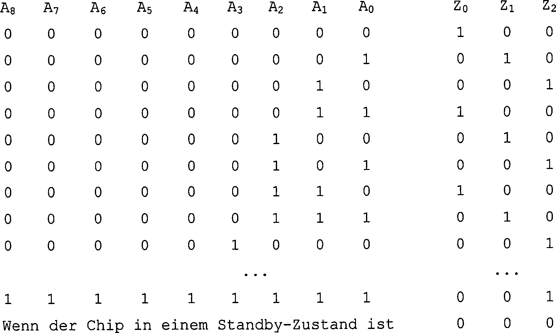
(Bezugsbeispiel 17)(Reference example 17)
Die Adressen A0 bis
A9 der Wortleitungen sind 10-Bit-Adressen.
Die Beziehung zwischen dem Ausgang der Überschussschaltung und der Eingangsadresse wird in der nachstehenden Tabelle 4 gezeigt.The relationship between the exit the excess circuit and the input address is shown in Table 4 below.
Tabelle
4 
(Bezugsbeispiel 18)(Reference example 18)
Bei dieser Ausführungsform werden X0, X2 und X2 und Y0, Y1 und Y2 mittels nMOS- und pMOS-Transistoren verbunden. Der nMOS-Transistor weist eine Gatelänge von LN und eine Gatebreite von WN auf, wohingegen der pMOS-Transistor eine Gatelänge von LP und eine Gatebreite von WP aufweist. Während ein CMOS mit einem nMOS und einem pMOS zum Übertragen aller Eingangsspannung ohne Unterscheidung mit einer Schwellenspannungen wirksam ist, kann die gleiche Wirkung erreicht werden, um ähnliche Ausgaben einfach mittels entweder eines nMOS oder eines pMOS zu erzeugen.In this embodiment, X 0 , X 2 and X 2 and Y 0 , Y 1 and Y 2 are connected by means of nMOS and pMOS transistors. The nMOS transistor has a gate length of LN and a gate width of WN, whereas the pMOS transistor has a gate length of LP and a gate width of WP. While a CMOS with an nMOS and a pMOS is effective for transmitting all input voltage without distinction with a threshold voltage, the same effect can be achieved to easily generate similar outputs using either an nMOS or a pMOS.
Die Beziehung zwischen Eingängen X0, X2 und X2 und Ausgängen Y0, Y1 und Y2 wird in der nachstehenden Tabelle 5 gezeigt.The relationship between inputs X 0 , X 2 and X 2 and outputs Y 0 , Y 1 and Y 2 is shown in Table 5 below.
Tabelle
5 
Wenn der Chip in einem Standby-Zustand
ist, sind alle Adressensignale Ai, Aj, /Ai und /Aj auf "L", so dass der erste
Eingang und der Ausgang der Schaltung A elektrisch voneinander isoliert
sind. Da der Ausgang der vierten Barrel-Schiebeeinrichtung in
Wenn der Chip aktiviert wird, wird entweder A0 oder /A0 auf "H" gebracht, und daher werden Z0, Z1 und Z2 von der Masse durch die Vorladeschaltung isoliert. Ihre Ausgangsknoten werden jedoch mit den Eingangspotentialen durch die damit in Reihe verbundene Barrel-Schiebeeinrichtung gemäß dem aktivierten Zustand verbunden, wobei das Ausgangspotential nicht instabil werden würde. Die Beziehung zwischen den Adressensignalen A0 bis A7 und den Ausgängen Z0, Z1 und Z2 der Überschussschaltung wird in der nachstehenden Tabelle 6 gezeigt.When the chip is activated, either A 0 or / A 0 is brought to "H", and therefore Z 0 , Z 1 and Z 2 are isolated from the ground by the precharge circuit. However, their output nodes are connected to the input potentials by the barrel shifter connected in series therewith in accordance with the activated state, and the output potential would not become unstable. The relationship between the address signals A 0 to A 7 and the outputs Z 0 , Z 1 and Z 2 of the excess circuit is shown in Table 6 below.
Tabelle
6 
(Bezugsbeispiel 19)(Reference example 19)
Bei dieser Anordnung wird jede der Barrel-Schiebeeinrichtungen mit einer Vorladeschaltung zum Halten der Ausgangsspannung auf einem festen Pegel in einem Standby-Zustand versehen. Genauer gesagt sind, wenn alle Eingangssignale Ai, Aj, /Ai und /Aj auf "L" sind, X0, X2 und X2 und Y0, Y1 und Y2 elektrisch voneinander isoliert, und nur die Ausgänge werden auf dem Massepotential gehalten. Die Beziehung zwischen den Adressen und den Ausgängen ist genau die selbe, wie diejenigen der Beispiele 14 bis 16.With this arrangement, each of the barrel shifters is provided with a precharge circuit for keeping the output voltage at a fixed level in a standby state. More specifically, when all input signals A i , A j , / A i and / A j are at "L", X 0 , X 2 and X 2 and Y 0 , Y 1 and Y 2 are electrically isolated from each other, and only that Outputs are kept at ground potential. The relationship between the addresses and the outputs is exactly the same as that of Examples 14 to 16.
Es sei bemerkt, dass mit der Schaltungskonfiguration dieser Ausführungsform die Gatelänge und die Gatebreite jeder der Schiebeeinrichtungen, die in Reihe verbunden sind, nicht notwendigerweise konstant gehalten werden. Das Verhältnis der Gatebreite W zu der Gatelänge L, oder β = W/L, ist normalerweise der Treiberkapazität des Transistors proportional, so dass die Verzögerungszeit von dem Eingang zu dem Ausgang der Überschussschaltung durch Verändern der Verhältnisse der vier in Reihe verbundenen Barrel-Schiebeeinrichtungen geringfügig für jede von ihnen verändert werden kann.It should be noted that with the circuit configuration this embodiment the gate length and the gate width of each of the shifters that are in series are not necessarily kept constant. The relationship the gate width W to the gate length L, or β = W / L, is usually proportional to the driver capacity of the transistor, so the delay time from the input to the output of the excess circuit by changing the conditions of the four barrel sliders connected in series slightly for each of changed them can be.
Genauer gesagt kann die Verzögerungszeit
durch Auswählen
von β-Werten
der pMOS-Transistoren der vier Barrel-Schiebeeinrichtungen A, B,
C und D minimiert werden, die in Reihe verbunden sind, um die folgende
Beziehung zu erfüllen.
βPA > βPB > βPC > βPD More specifically, the delay time can be minimized by selecting β values of the pMOS transistors of the four barrel shifters A, B, C and D connected in series to satisfy the following relationship.
β PA > β PB > β PC > β PD
Dies ist so, da jede der Barrel-Schiebeeinrichtungen ihre eigene elektrische Kapazität aufweist, und daher steigt die elektrische Ladung, der ein Durchlaufen ermöglicht werden muss, um von "L" in dem Vorladezustand auf "H" für einen ausgewählten Zustand aufzuladen, mit den Abständen von den Ausgängen Z0, Z1 und Z2 an.This is because each of the barrel shifters has its own electrical capacity, and therefore, the electrical charge that must be allowed to go through to charge from "L" in the precharge state to "H" for a selected state increases with the distances from the outputs Z 0 , Z 1 and Z 2 .
Es sei bemerkt, dass die Betriebsgeschwindigkeit
des nMOS-Transistors sich bei diese Ausführungsform nicht auf β bezieht.
Somit kann die folgende Beziehung erfüllt werden.
βNA > βNB > βNC > βND Note that the operating speed of the nMOS transistor does not refer to β in this embodiment. Thus, the following relationship can be satisfied.
β NA > β NB > β NC > β ND
(Bezugsbeispiel 20)(Reference example 20)
Bei dieser Anordnung werden die Ausgänge der Schaltung A des Beispiels 14 als Eingang an die Barrel-Schiebe einrichtungen vom Beispiel 18 angelegt. Die Beziehung zwischen den Adressenausgaben ist genau die gleiche wie diejenige bei den Beispielen 14 bis 17.With this arrangement, the outputs of the Circuit A of Example 14 as an input to the barrel sliding devices from Example 18. The relationship between the address outputs is exactly the same as that in Examples 14 to 17.
(Bezugsbeispiel 21)(Reference example 21)
Im Gegensatz zu den Beispielen 18 bis 20, bei denen 2-Bit-Adressen an eine Barrel-Schiebeeinrichtung angelegt werden, hat diese Beispiel Barrel-Schiebeeinrichtungen, die eine Eins-zu-eins-Korrespondenz mit den Adressen zeigen.In contrast to Examples 18 to 20, where 2-bit addresses can be applied to a barrel sliding device, this example Barrel pushers that have a one-to-one correspondence show the addresses.
Es sei jedoch bemerkt, dass zwei Arten von Schiebeeinrichtungen vorgesehen sind. Eine erste Schiebeeinrichtung S1 verschiebt die Ausgang um +1 bezüglich des Eingangs für die Adresse Ai = "1" (Y2 = X2, Y1 = X0, Y0 = X2) , wobei jedoch der Ausgang bezüglich des Eingangs für die Adresse Ai = "0" (Y2 = X2, Y1 = X2, Y0 = X0) nicht verschoben wird, und eine zweite Schiebeeinrichtung S2 verschiebt den Ausgang um –1 bezüglich des Eingangs für die Adresse Ai = "1" (Y2 = X0, Y1 = X2, Y0 = X2) , wobei jedoch der Ausgang bezüglich des Eingangs nicht verschoben wird, wenn die Adresse Ai = "0" ist.However, it should be noted that two types of pushers are provided. A first shifter S1 shifts the output by +1 with respect to the input for the address A i = "1" (Y 2 = X 2 , Y 1 = X 0 , Y 0 = X 2 ), but the output with respect to the input for the address A i = "0" (Y 2 = X 2 , Y 1 = X 2 , Y 0 = X 0 ) is not shifted, and a second shifter S2 shifts the output by -1 with respect to the input for the address A i = "1" (Y 2 = X 0 , Y 1 = X 2 , Y 0 = X 2 ), but the output is not shifted with respect to the input if the address A i = "0".
Die erste Schiebeeinrichtungen S1
wird für
geradzahlige Adressen (A0, A2,
A4, A6) verwendet,
wohingegen die zweite Schiebeeinrichtung S2 für ungeradzahlige Adressen (A1, A3, A5,
A7) verwendet wird.
Wie in dem Fall von Beispiel 18 wird eine Vorladeschaltung an der Endstufe (Z0, Z1, Z2) des Ausgangs der Überschussschaltung bereitgestellt. Wenn der Chip in einem Standby-Zustand ist, wird die Beziehung von Z2 = Z1 = Z0 = "L" sichergestellt. Es sei jedoch bemerkt, dass die einzige Vorladeschaltung durch einzelne Vorladungsschaltungen, wie in dem Fall von Beispiel 19, ersetzt werden kann.As in the case of Example 18, a precharge circuit is provided at the output stage (Z 0 , Z 1 , Z 2 ) of the output of the excess circuit. When the chip is in a standby state, the relationship of Z 2 = Z 1 = Z 0 = "L" is ensured. However, it should be noted that the single precharge circuit can be replaced with individual precharge circuits, as in the case of Example 19.
Claims (13)
Applications Claiming Priority (4)
| Application Number | Priority Date | Filing Date | Title |
|---|---|---|---|
| JP8345495 | 1995-03-16 | ||
| JP8345495 | 1995-03-16 | ||
| JP08717095A JP3281215B2 (en) | 1995-03-16 | 1995-04-12 | Dynamic semiconductor memory device |
| JP8717095 | 1995-04-12 |
Publications (2)
| Publication Number | Publication Date |
|---|---|
| DE69629068D1 DE69629068D1 (en) | 2003-08-21 |
| DE69629068T2 true DE69629068T2 (en) | 2004-04-22 |
Family
ID=26424470
Family Applications (1)
| Application Number | Title | Priority Date | Filing Date |
|---|---|---|---|
| DE69629068T Expired - Fee Related DE69629068T2 (en) | 1995-03-16 | 1996-03-14 | A semiconductor memory device |
Country Status (5)
| Country | Link |
|---|---|
| US (1) | US5761109A (en) |
| EP (1) | EP0732700B1 (en) |
| JP (1) | JP3281215B2 (en) |
| KR (1) | KR100236215B1 (en) |
| DE (1) | DE69629068T2 (en) |
Families Citing this family (24)
| Publication number | Priority date | Publication date | Assignee | Title |
|---|---|---|---|---|
| US5687114A (en) | 1995-10-06 | 1997-11-11 | Agate Semiconductor, Inc. | Integrated circuit for storage and retrieval of multiple digital bits per nonvolatile memory cell |
| US5870335A (en) | 1997-03-06 | 1999-02-09 | Agate Semiconductor, Inc. | Precision programming of nonvolatile memory cells |
| US6487116B2 (en) | 1997-03-06 | 2002-11-26 | Silicon Storage Technology, Inc. | Precision programming of nonvolatile memory cells |
| JPH11110967A (en) * | 1997-10-01 | 1999-04-23 | Nec Corp | Semiconductor memory device |
| US5917744A (en) * | 1997-12-18 | 1999-06-29 | Siemens Aktiengesellschaft | Semiconductor memory having hierarchical bit line architecture with interleaved master bitlines |
| US6282145B1 (en) | 1999-01-14 | 2001-08-28 | Silicon Storage Technology, Inc. | Array architecture and operating methods for digital multilevel nonvolatile memory integrated circuit system |
| JP2001084785A (en) * | 1999-09-17 | 2001-03-30 | Nec Corp | Sense amplifier circuit and semiconductor memory |
| US6396742B1 (en) | 2000-07-28 | 2002-05-28 | Silicon Storage Technology, Inc. | Testing of multilevel semiconductor memory |
| US6327169B1 (en) * | 2000-10-31 | 2001-12-04 | Lsi Logic Corporation | Multiple bit line memory architecture |
| JP2002216471A (en) * | 2001-01-17 | 2002-08-02 | Mitsubishi Electric Corp | Semiconductor memory device |
| US6456521B1 (en) * | 2001-03-21 | 2002-09-24 | International Business Machines Corporation | Hierarchical bitline DRAM architecture system |
| FR2830365B1 (en) * | 2001-09-28 | 2004-12-24 | St Microelectronics Sa | DYNAMIC VIVE MEMORY |
| JP3696144B2 (en) | 2001-10-17 | 2005-09-14 | 株式会社東芝 | Semiconductor memory device |
| US6836427B2 (en) * | 2002-06-05 | 2004-12-28 | Micron Technology, Inc. | System and method to counteract voltage disturbances in open digitline array dynamic random access memory systems |
| JP3806084B2 (en) | 2002-12-25 | 2006-08-09 | 株式会社東芝 | Ferroelectric memory and data read method thereof |
| TWI281159B (en) * | 2003-03-21 | 2007-05-11 | Mediatek Inc | Sense out circuit for single-bitline semiconductor memory device |
| US7254074B2 (en) * | 2005-03-07 | 2007-08-07 | Micron Technology, Inc. | Open digit line array architecture for a memory array |
| KR100780954B1 (en) * | 2006-08-04 | 2007-12-03 | 삼성전자주식회사 | Sense amplifier and semiconductor memory device comprising it, and data sensing method |
| US20080056041A1 (en) * | 2006-09-01 | 2008-03-06 | Corvin Liaw | Memory circuit |
| DE102007012902B3 (en) * | 2007-03-19 | 2008-07-10 | Qimonda Ag | Bit line pair and amplifier arrangement for use in e.g. dynamic RAM, of computer system, has read amplifiers whose positions along bit line direction are selected such that coupling paths have same coupling characteristics |
| US8085611B2 (en) * | 2009-01-22 | 2011-12-27 | Macronix International Co., Ltd. | Twisted data lines to avoid over-erase cell result coupling to normal cell result |
| JP2011048885A (en) * | 2009-08-28 | 2011-03-10 | Renesas Electronics Corp | Semiconductor memory device |
| KR20140079447A (en) | 2011-10-04 | 2014-06-26 | 컨버전트 인텔렉츄얼 프로퍼티 매니지먼트 인코포레이티드 | Reduced noise dram sensing |
| CN116206648B (en) * | 2022-01-27 | 2024-02-20 | 北京超弦存储器研究院 | Dynamic memory, read-write method thereof and memory device |
Family Cites Families (7)
| Publication number | Priority date | Publication date | Assignee | Title |
|---|---|---|---|---|
| US4656613A (en) * | 1984-08-29 | 1987-04-07 | Texas Instruments Incorporated | Semiconductor dynamic memory device with decoded active loads |
| JPS62202397A (en) * | 1986-02-28 | 1987-09-07 | Fujitsu Ltd | Semiconductor storage device |
| US5214601A (en) * | 1986-12-11 | 1993-05-25 | Mitsubishi Denki Kabushiki Kaisha | Bit line structure for semiconductor memory device including cross-points and multiple interconnect layers |
| JP3076606B2 (en) * | 1990-12-14 | 2000-08-14 | 富士通株式会社 | Semiconductor memory device and inspection method thereof |
| JP3302796B2 (en) * | 1992-09-22 | 2002-07-15 | 株式会社東芝 | Semiconductor storage device |
| JP3440335B2 (en) * | 1993-08-18 | 2003-08-25 | 日本テキサス・インスツルメンツ株式会社 | Semiconductor memory device |
| KR100215595B1 (en) * | 1993-09-21 | 1999-08-16 | 니시무로 타이죠 | Dynamic semiconductor memory device |
-
1995
- 1995-04-12 JP JP08717095A patent/JP3281215B2/en not_active Expired - Fee Related
-
1996
- 1996-03-13 US US08/614,537 patent/US5761109A/en not_active Expired - Fee Related
- 1996-03-14 EP EP96301737A patent/EP0732700B1/en not_active Expired - Lifetime
- 1996-03-14 DE DE69629068T patent/DE69629068T2/en not_active Expired - Fee Related
- 1996-03-16 KR KR1019960007096A patent/KR100236215B1/en not_active IP Right Cessation
Also Published As
| Publication number | Publication date |
|---|---|
| EP0732700A3 (en) | 1996-10-30 |
| US5761109A (en) | 1998-06-02 |
| KR960035632A (en) | 1996-10-24 |
| JP3281215B2 (en) | 2002-05-13 |
| DE69629068D1 (en) | 2003-08-21 |
| EP0732700B1 (en) | 2003-07-16 |
| KR100236215B1 (en) | 1999-12-15 |
| EP0732700A2 (en) | 1996-09-18 |
| JPH08315577A (en) | 1996-11-29 |
Similar Documents
| Publication | Publication Date | Title |
|---|---|---|
| DE69629068T2 (en) | A semiconductor memory device | |
| DE4206832C2 (en) | Non-volatile semiconductor memory device | |
| DE4433695C2 (en) | Dynamic semiconductor memory device | |
| DE4211844C2 (en) | Semiconductor memory device | |
| DE2919166C2 (en) | Storage device | |
| DE4308665B4 (en) | DRAM with a bidirectional global bitline | |
| DE10196802B4 (en) | Noise reduction for open bit-line DRAM architectures | |
| DE2650479C2 (en) | Storage arrangement with charge storage cells | |
| EP0908893B1 (en) | Multiplane memory architecture | |
| DE4222273C2 (en) | Two-channel memory and method for data transmission in such | |
| EP0393435B1 (en) | Static memory cell | |
| DE3247538C2 (en) | ||
| DE3838942C2 (en) | ||
| DE3827287A1 (en) | SEMICONDUCTOR MEMORY DEVICE | |
| DE10135782A1 (en) | Semiconductor memory device | |
| DE3923629A1 (en) | SEMICONDUCTOR STORAGE DEVICE | |
| DE10305822A1 (en) | Semiconductor memory device | |
| DE4138340C2 (en) | Semiconductor memory device and method for operating such a device | |
| DE4022149C2 (en) | ||
| DE3744451A1 (en) | Device for loading a static read-write memory (SRAM) | |
| DE10144245B4 (en) | Semiconductor memory device with bit lines and a sense amplifier | |
| DE4024295A1 (en) | DYNAMIC SEMICONDUCTOR STORAGE DEVICE | |
| DE19756929B4 (en) | Cell array and sense amplifier structure with improved noise characteristics and reduced size | |
| DE3104880C2 (en) | Random access memory | |
| EP1119859B1 (en) | Dual-port memory location |
Legal Events
| Date | Code | Title | Description |
|---|---|---|---|
| 8364 | No opposition during term of opposition | ||
| 8339 | Ceased/non-payment of the annual fee |