Die
vorliegende Erfindung bezieht sich auf einen Mikro- Beschleunigungssensor
aus einem Halbleiter.The
The present invention relates to a micro-acceleration sensor
from a semiconductor.
Ein
herkömmlicher
Halbleiterbeschleunigungssensor ist in den 12A und 12B gezeigt. 12A ist eine perspektivische
Ansicht und 12B ist
ein Schaltkreisdiagramm. In 12A umfaßt der Halbleiterbeschleunigungssensor
ein viereckiges, prismaförmiges,
dickes Gewicht 10 aus einem Halbleiter mit einer Dicke
von zum Beispiel 400 μm,
ein dickes Trägerelement 12,
das durch eine vorgegebene Lücke
von dem Gewicht 10 getrennt ist und so geformt ist, das
es dieses umgibt, und einen dünnen
Balken 11, der eine Seitenfläche des Gewichts 10 mit
derjenigen des Trägerelements 12 verbindet,
die der einen Seitenfläche
gegenüberliegt, und
der eine Dicke von zum Beispiel 10 bis 40 μm besitzt. Dehnungmeßstreifen 31, 32, 33 und 34 sind
auf der oberen Seitenfläche
des Balkens 11 geformt. Die Dehnungsmeßstreifen 31 und 33 sind
in der Verbindungsseite mit dem Gewicht 10 in der longitudinalen Richtung
des Balkens 11 geformt, und die Dehnungsmeßstreifen 32 und 34 sind
in der Querrichtung des Balkens 11 geformt. Diese Dehnungsmeßstreifen 31 bis 34 sind
elektrisch wie in 12B verbunden
und bilden eine Wheatstone-Brücke,
in der die Dehnungsmeßstreifen 31 und 33 sowie 32 und 34 jeweils einander
gegenüberliegen.
In 12B bezeichnet V eine
Spannungsversorgung, und S1 und S2 bezeichnen Signalausgabeanschlüsse.A conventional semiconductor acceleration sensor is shown in FIGS 12A and 12B shown. 12A is a perspective view and 12B is a circuit diagram. In 12A For example, the semiconductor acceleration sensor comprises a square, prism-shaped, thick weight 10 of a semiconductor having a thickness of, for example, 400 μm, a thick support element 12 that by a given gap of the weight 10 is separated and shaped so that it surrounds this, and a thin beam 11 that has a side surface of weight 10 with that of the carrier element 12 which faces the one side surface and has a thickness of, for example, 10 to 40 μm. Dehnungmeßstreifen 31 . 32 . 33 and 34 are on the upper side surface of the beam 11 shaped. The strain gauges 31 and 33 are in the connection side with the weight 10 in the longitudinal direction of the beam 11 shaped, and the strain gauges 32 and 34 are in the transverse direction of the beam 11 shaped. These strain gauges 31 to 34 are electric as in 12B connected and form a Wheatstone bridge, in which the strain gauges 31 and 33 such as 32 and 34 each opposite each other. In 12B V indicates a power supply, and S 1 and S 2 indicate signal output terminals.
Wenn
eine Beschleunigung in der vertikalen Richtung (welches die Richtung
der Beschleunigungsmessung ist) auf das Gewicht 10 wirkt,
wirkt auf das Gewicht 10 eine Kraft in der vertikalen Richtung,
und der Balken 11 biegt sich in die durch den Pfeil P gekennzeichnete
Richtung. Zu diesem Zeitpunkt wirkt eine Zugspannung auf die obere
Seite des Balkens 11, so daß der Widerstand jeder der Dehnungsmeßstreifen 31 und 33,
die in der longitudinalen Richtung des Balkens 11 geformt
sind, zunimmt und sich demgegenüber
der Widerstand jeder der Dehnungsmeßstreifen 32 und 34,
die in der Querrichtung des Balkens 11 geformt sind, nicht ändert. Dies
bewirkt, daß ein
Detektionssignal, dessen Pegel proportional dem Betrag der Beschleunigung
ist, von den Signalausgabeanschlüssen
S1 und S2 der Wheatstone-Brücke ausgegeben
wird.When an acceleration in the vertical direction (which is the direction of the acceleration measurement) is based on the weight 10 acts, affects the weight 10 a force in the vertical direction, and the beam 11 bends in the direction indicated by the arrow P direction. At this time, a tensile stress acts on the upper side of the beam 11 so that the resistance of each of the strain gauges 31 and 33 which are in the longitudinal direction of the beam 11 are formed, and in contrast increases the resistance of each of the strain gauges 32 and 34 in the transverse direction of the beam 11 are shaped, do not change. This causes a detection signal whose level is proportional to the amount of acceleration to be output from the signal output terminals S 1 and S 2 of the Wheatstone bridge.
Wegen
der Konfiguration, bei der das Gewicht 10 nur an einem
Ende gehalten wird, besitzt der Halbleiterbeschleunigungssensor
eine ungleiche Stoßfestigkeit.
Wie in 13 gezeigt, ist
daher ein solcher Halbleiterbeschleunigungssensor überlicherweise
in einem hermetisch abgeschlossenen Behälter 850 untergebracht,
welcher eine Dämpfungsflüssigkeit 830 enthält. In 13 bezeichnet 800 den Halbleiterbe schleunigungssensor
und 820 bezeichnet einen Verstärker zur Signaldetektion.Because of the configuration in which the weight 10 is held only at one end, the semiconductor acceleration sensor has an uneven impact resistance. As in 13 Therefore, such a semiconductor acceleration sensor is usually in a hermetically sealed container 850 accommodated, which is a damping fluid 830 contains. In 13 designated 800 the semiconductor acceleration sensor and 820 denotes an amplifier for signal detection.
In
dem oben beschriebenen Halbleiterbeschleunigungssensor, wie er in 14 gezeigt ist, ist die
Biegungsmittelpunktslinie 13 des Balkens 11 um einen
Abstand L von dem Schwerpunkt des Gewichts 10 entfernt.
Wenn eine Beschleunigung in der transversalen Richtung (die nicht
die Richtung der Beschleunigungsmessung ist) auf das Gewicht 10 wirkt, wird
ein durch den Pfeil M angezeigtes Drehmoment durch diese Beschleunigung
und den Abstand L erzeugt, das auf das Gewicht 10 wirkt,
so daß auf
das Gewicht 10 eine Kraft in der vertikalen Richtung auf die
gleiche Weise wirkt, wie in dem Fall, in dem eine vertikale Beschleunigung
wirkt, wodurch der Balken 11 in die durch den Pfeil P gezeigte
Richtung gebogen wird. Diese Biegung bewirkt, daß die Wheatstone-Brücke ein
Signal ausgibt, und diese Signalausgabe ist eine Störausgabe,
die die Detektionsgenauigkeit beeinträchtigt.In the above-described semiconductor acceleration sensor as shown in FIG 14 is the bend center point line 13 of the beam 11 by a distance L from the center of gravity of the weight 10 away. When an acceleration in the transverse direction (which is not the direction of the acceleration measurement) on the weight 10 acts, a torque indicated by the arrow M is generated by this acceleration and the distance L, which is based on the weight 10 affects, so on the weight 10 a force acts in the vertical direction in the same manner as in the case where a vertical acceleration acts, whereby the beam 11 is bent in the direction shown by the arrow P. This bend causes the Wheatstone bridge to output a signal, and this signal output is a spurious output which interferes with the detection accuracy.
Als
eine Gegenmaßnahme
zu diesem Problem kann eine Kon figuration vorgeschlagen werden,
in der, wie in 15 gezeigt,
ein zusätzliches Gewicht 14 aus
Glas oder dergleichen mit der oberen Fläche des Gewichts 10 verbunden
ist, so daß der Schwerpunkt
G des Gewichts aus dem Gewicht 10 und dem zusätzlichen
Gewicht 14 auf der Biegemittelpunktslinie 13 des
Balkens 11 liegt, wodurch der Abstand L auf Null reduziert
wird. Jedoch besitzt diese verbesserte Konstruktion insofern einen
Nachteil, als ein zusätzlicher
Prozeßschritt zum
Befestigen des zusätzlichen
Gewichts erforderlich ist und somit die Produktionskosten zunehmen.As a countermeasure to this problem, a configuration may be proposed in which, as in 15 shown an extra weight 14 glass or the like with the upper surface of the weight 10 is connected so that the center of gravity G of the weight from the weight 10 and the extra weight 14 at the midpoint of the bend 13 of the beam 11 which reduces the distance L to zero. However, this improved construction has a drawback in that an additional process step for attaching the additional weight is required, thus increasing the production cost.
Bei
der Herstellung eines Halbleiterbeschleunigungssensors, wie in 12 oder 15 gezeigt,
werden das Gewicht 10, das Trägerelement 12 und
der Balken 11 durch Ätzen
sowohl der oberen als auch der unteren Flächen eines Halbleitersubstrats unter
Verwendung eines Geräts,
wie etwa einer Plasmaätzvorrichtung,
erzeugt. Bei einem solchen Plasmaätzvorgang geht das Ätzen, wegen
der entsprechenden Arbeitsmerkmale, mit einer hohen Geschwindigkeit
vonstatten, wenn die Arbeitsbreite groß ist, und es geht mit einer
niedrigen Geschwindigkeit vonstatten, wenn die Arbeitsbreite klein
ist. In dem Fall, daß unterschiedliche
Arbeitsbreiten in einem zu bearbeitenden Halbleitersubstrat existieren, wie
in 16 durch W3 und W4 angezeigt,
resultieren daraus unterschiedliche Ätztiefen, wie durch D3 und D4 angezeigt.
Dies erzeugt insofern ein Problem, als die Genauigkeit des Ätzvorgangs
verringert wird, wobei die Prozeßausbeute verringert wird.In the manufacture of a semiconductor acceleration sensor, as in 12 or 15 shown will be the weight 10 , the carrier element 12 and the beam 11 by etching both the upper and lower surfaces of a semiconductor substrate using an apparatus such as a plasma etching apparatus. In such a plasma etching process, because of the corresponding working characteristics, the etching proceeds at a high speed when the working width is large, and it proceeds at a low speed when the working width is small. In the case that different working widths exist in a semiconductor substrate to be processed, as in FIG 16 indicated by W 3 and W 4 , resulting in different etch depths, as indicated by D 3 and D 4 . This creates a problem in that the accuracy of the etching process is reduced, thereby reducing the process yield.
Um
die Stoßfestigkeit
zu verbessern, sind die oben beschriebenen Halbleiterbeschleunigungssensoren üblicherweise
in einem hermetisch abgeschlossenen Gehäuse untergebracht, welches
eine Dämpfungsflüssigkeit
enthält.
Das Vorhandensein einer Dämpfungsflüssigkeit
bewirkt eine Verringerung der Detektionsempfindlichkeit, und daher
ist es erforderlich, die Reduktionsrate abzuschätzen und die Empfindlichkeit
vor Einführen
der Dämpfungsflüssigkeit
in den Behälter
einzustellen. Da die Viskosität und
die Kompressibilität
der Dämpfungsflüssigkeit sich
abhängig
von Druck und Temperatur än dern, ändert sich
die Empfindlichkeit, was ein weiteres Problem mit sich bringt, daß nämlich die
Produktionsausbeute ungleichmäßig ist.In order to improve the impact resistance, the semiconductor accelerations described above are usually housed in a hermetically sealed housing containing a damping fluid. The presence of a damping fluid causes a reduction in the detection sensitivity, and therefore, it is necessary to estimate the reduction rate and adjust the sensitivity before introducing the damping fluid into the reservoir. Since the viscosity and the compressibility of the damping fluid vary depending on pressure and temperature, the sensitivity changes, causing another problem that the production yield is uneven.
Die 22 und 23 zeigen einen weiteren herkömmlichen
Halbleiterbeschleunigungssensor als Beispiel: 22 ist eine Draufsicht, und 23 ist eine Seitenansicht.
Wie in den 22 und 23 gezeigt, umfaßt der Halbleiterbeschleunigungssensor ein
dickwandiges, quadratisches Gewicht 901, das zum Beispiel
400 μm dick
ist, einen dickwandigen Träger 906,
der in einem vorgegebenen Abstand von einer Seite des Gewichts angeordnet
ist, und einen dünnwandigen
Balken 907, der zum Beispiel 20–40 μm dick ist, wobei der Balken
eine Seite des Gewichts 901 mit einer gegenüberliegenden
Seite des Trägers 906 verbindet.
In dem Balken 907 sind Dehnungsmeßstreifen 907A, 907B, 907C, 907D geformt. Die
Dehnungsmeßstreifen 907A, 907C sind
in der oberen Fläche
der Verbindung zwischen dem Balken 907 und dem Träger 906 in
der Längsrichtung
des Balkens 907 geformt, während die Dehnungsmeßstreifen 907B, 907D in
der oberen Fläche
der Verbindung zwischen dem Balken 907 und dem Gewicht 901 in
der Querrichtung des Balkens 907 geformt sind. Diese Dehnungsmeßstreifen 907A, 907B, 907C, 907D werden
zum Bilden einer Wheatstone-Brücke verwendet,
indem die Dehnungsmeßstreifen 907A, 907C sowie 907B, 907D einander
gegenüberliegend
angeordnet sind, wie in 26 gezeigt. In
diesem Fall bezeichnet E einen Spannungsversorgungsanschluß, G einen
Masseanschluß und
S1, S2 Signalausgabeanschlüsse.The 22 and 23 show another conventional semiconductor acceleration sensor as an example: 22 is a top view, and 23 is a side view. As in the 22 and 23 As shown, the semiconductor acceleration sensor comprises a thick-walled, square weight 901 which is, for example, 400 μm thick, a thick-walled carrier 906 which is arranged at a predetermined distance from one side of the weight, and a thin-walled beam 907 which is, for example, 20-40 μm thick, with the bar one side of the weight 901 with an opposite side of the carrier 906 combines. In the beam 907 are strain gauges 907A . 907B . 907C . 907D shaped. The strain gauges 907A . 907C are in the upper surface of the connection between the beam 907 and the carrier 906 in the longitudinal direction of the beam 907 shaped while the strain gauges 907B . 907D in the upper surface of the connection between the beam 907 and the weight 901 in the transverse direction of the beam 907 are shaped. These strain gauges 907A . 907B . 907C . 907D are used to form a Wheatstone bridge by the strain gauges 907A . 907C such as 907B . 907D are arranged opposite each other, as in 26 shown. In this case, E denotes a power supply terminal, G a ground terminal, and S1, S2 signal output terminals.
Wenn
eine Beschleunigung auf das Gewicht 901 in der Richtung
des Pfeiles V in 23 wirkt,
als in einer Richtung senkrecht zum Gewicht 901 (die Richtung,
in der die Beschleunigung festgestellt wird), erfährt das
Gewicht 901 eine vertikale Kraft Fv, was ein Herunterbiegen
des Balkens in Richtung des Pfeiles M bewirkt, wie in 27 gezeigt. Zu diesem Zeitpunkt
wirkt eine Zugspannung auf die obere Oberfläche der Verbindung zwischen
dem Balken 907 und dem Träger 906 und auf die
der Verbindung zwischen dem Balken 907 und dem Gewicht 901.
Als Ergebnis nimmt der Widerstand der Dehnungsmeßstreifen 907A, 907C,
die in der Längsrichtung
des Balkens geformt sind, zu, wohingegen derjenige der Dehnungsmeßstreifen 907B, 907D,
die in der Querrichtung geformt sind, unverändert bleibt. Es werden also
Detektionssignale, deren Wert proportional der Beschleunigung ist,
von den Ausgabeanschlüssen S1,
S2 der Wheatstone-Brücke
ausgegeben.If an acceleration on the weight 901 in the direction of the arrow V in 23 acts as in a direction perpendicular to the weight 901 (the direction in which the acceleration is detected) experiences the weight 901 a vertical force Fv, causing the beam to bend down in the direction of arrow M, as in FIG 27 shown. At this time, a tensile stress acts on the upper surface of the connection between the beam 907 and the carrier 906 and on the connection between the beam 907 and the weight 901 , As a result, the resistance of the strain gauges decreases 907A . 907C , which are formed in the longitudinal direction of the beam to, whereas that of the strain gauges 907B . 907D which are shaped in the transverse direction, remains unchanged. Thus, detection signals whose value is proportional to the acceleration are output from the output terminals S1, S2 of the Wheatstone bridge.
Da
eine normale Diffusionstechnik zum Herstellen der Dehnungsmeßstreifen 907A, 907B, 907C, 907D verwendet
wird, sind die Oberflächen
des Gewichts 901, des Balkens 907 und des Trägers 906 mit einem
Passivierungsfilm 910 aus SiO2,
SiN oder dergleichen bedeckt, um diese zu schützen.As a normal diffusion technique for making the strain gauges 907A . 907B . 907C . 907D used are the surfaces of the weight 901 , the beam 907 and the vehicle 906 with a passivation film 910 made of SiO 2 , SiN or the like to protect them.
Da
es einen Abstand L von der Spannungsmittellinie 909 des
Balkens 907 bis zum Schwerpunkt W des Gewichts 901 im
Beschleunigungssensor der 23 gibt,
erzeugen der Abstand L von der Spannungsmittellinie 909 zum
Schwerpunkt W des Gewichts 901 und die Querkraft Fh, die
in dem Gewicht 901 aufgrund der Beschleunigung erzeugt
wird, ein Drehmoment, wenn die Beschleunigung quer auf das Gewicht 901 wirkt
(die Rich tung, in der die Beschleunigung nicht festgestellt wird),
wie durch den Pfeil H gezeigt. Demzufolge wird ein Herunterbiegen
des Balkens 907 in Richtung des Pfeiles M bewirkt, wie
in dem Falle, in dem die Beschleunigung vertikal auf den Balken 907 wirkt.
In Abhängigkeit
von der Spannung gibt die Wheatstone-Brücke ein Signal aus, das eine
Störausgabe
bildet und die Meßgenauigkeit
verringert.As there is a distance L from the stress line 909 of the beam 907 to the center of gravity W of the weight 901 in the acceleration sensor the 23 gives the distance L from the stress centerline 909 to the center of gravity W of the weight 901 and the lateral force Fh that is in the weight 901 due to the acceleration is generated, a torque when the acceleration is transverse to the weight 901 acts (the direction in which the acceleration is not detected), as shown by the arrow H. As a result, the beam will turn down 907 in the direction of the arrow M causes, as in the case in which the acceleration vertically on the beam 907 acts. Depending on the voltage, the Wheatstone bridge outputs a signal that forms a spurious output and reduces the accuracy of measurement.
Aus
dem oben angegebenen Grund kann es als hilfreich er achtet werden,
den Abstand L auf Null zu verringern, indem ein zusätzliches
Gewicht 908, wie etwa Glas, auf der oberen Oberfläche des
Gewichts 901 hinzugefügt
wird, um den Schwerpunkt W der Kombination von Gewicht 901 und
dem zusätzlichen
Gewicht 908 mit der Spannungsmittellinie 909 des
Balkens 907 zusammenfallen zu lassen; jedoch wird der zusätzliche
Verfahrensschritt zum Verbinden der beiden Gewichte die Kosten weiter
erhöhen.For the reason given above, it may be helpful to reduce the distance L to zero by adding extra weight 908 , such as glass, on the upper surface of the weight 901 is added to the center of gravity W of the combination of weight 901 and the extra weight 908 with the stress line 909 of the beam 907 to collapse; however, the additional process step of connecting the two weights will further increase costs.
Ein
weiteres. Problem, das mit dem oben erwähnten Beschleunigungssensor
verbunden ist, ist eine geringe Meßempfindlichkeit, da die in
der oberen Oberfläche
der Verbindung zwischen dem Balken und dem Gewicht in der Querrichtung
des Balkens geformten Dehnungsmeßstreifen keine Widerstandsänderungen
erzeugen, wenn eine Beschleunigung wirkt.One
additional. Problem with the above-mentioned acceleration sensor
is connected, is a low sensitivity, since the in
the upper surface
the connection between the beam and the weight in the transverse direction
The bar formed strain gauges no resistance changes
generate when an acceleration acts.
Darüberhinaus
wird der Passivierungsfilm aus SiO2, SiN
oder dergleichen für
den Schutz der Dehnungsmeßstreifen
normalerweise bei hohen Temperaturen verarbeitet bevor wieder die
normale Temperatur eingestellt wird. Der Unterschied in den thermischen
Ausdehnungskoeffizienten des Passivierungsfilms und des Halbleiters
Silizium kann aufgrund der auf der Oberfläche des Halbleiters Silizium erzeugten
Spannung, wenn wieder die normale Temperatur eingestellt wird, ein
Biegen des Balkens 7 bewirken, wie in 29 gezeigt. Die Situation, in der eine
Beschleunigung angelegt wurde, wird erreicht, wenn der Balken gebogen
wird und eine Spannung von der Wheatstone-Brücke ausgegeben wird. Diese Spannung
wird Offset-Spannung genannt und verringert nicht nur das Signal/Rauschverhältnis der
Sensorausgabe sondern auch die Messgenauigkeit.Moreover, the passivation film of SiO 2 , SiN or the like for protection of the strain gages is normally processed at high temperatures before the normal temperature is restored. The difference in the coefficients of thermal expansion of the passivation film and the semiconductor silicon may, due to the voltage generated on the surface of the semiconductor silicon when the normal temperature is restored, cause the beam to bend 7 cause, as in 29 shown. The situation in which An acceleration is applied when the beam is bent and a voltage is output from the Wheatstone bridge. This voltage is called the offset voltage and not only reduces the signal-to-noise ratio of the sensor output but also the measurement accuracy.
Aus
der US 4,553,436 ist
ein Beschleunigungsmesser aus Silizium bekannt, der dem Oberbegriff
von Anspruch 1 entspricht. Hier ist eine zentrale Masse an ihren
Ecken durch vier flexible jeweils senkrecht zueinander angeordnete
Träger
gehalten. An dem jeweils festen Ende eines Trägers ist ein Wiederstandselement
angeordnet. Jedes Wiederstandselement kann zwei parallele Teile
aufweisen, um so ein kompaktes Wiederstandselement zur Verfügung zu
stellen.From the US 4,553,436 An accelerometer made of silicon is known, which corresponds to the preamble of claim 1. Here, a central mass is held at its corners by four flexible carriers arranged perpendicular to one another. At the respective fixed end of a carrier, a resistance element is arranged. Each resistance element may have two parallel parts so as to provide a compact resistance element.
Aus
der DE 30 09 091 ist
eine Messfederplatte mit einem zentralen Teil bekannt, der über Messfeldern
mit dem Randgebiet der Platte zusammenhängt. Auf den Messfeldern sind
Dehnungsmessstreifen angeordnet. Die Messfederplatte kann in ihrem
zentralen Teil eine Last aufnehmen.From the DE 30 09 091 a measuring spring plate with a central part is known, which is connected via measuring fields with the edge region of the plate. Strain gauges are arranged on the measuring fields. The measuring plate can take a load in its central part.
Aus
der US 4,641,539 ist
ein Kraftsensor bekannt. Ein Kraftaufnahmeelement ist mit einem Grundkörper über vier
Tragelemente verbunden. Die Tragelemente weisen Messglieder auf,
die auf eine Deformation der selben reagieren. Ein nicht unterbrochener
Leiterpfad führt über jede
der Tragelemente.From the US 4,641,539 a force sensor is known. A force receiving element is connected to a base body via four support elements. The support elements have measuring members that respond to a deformation of the same. An uninterrupted conductor path leads over each of the support elements.
Es
ist die Aufgabe der vorliegenden Erfindung, einen Beschleunigungssensor
zur Verfügung zu
stellen, der so ausgeführt
ist, dass er die Offset-Spannung verringert.It
The object of the present invention is an acceleration sensor
available too
put that way
is that it reduces the offset voltage.
Diese
und weitere Aufgaben werden erfindungsgemäß durch den in den beigefügten Patentansprüchen definierten
Halbleiterbeschleunigungssensor gelöst.These
and further objects are inventively defined by the appended claims
Semiconductor acceleration sensor solved.
Entsprechend
der Erfindung ist ein Halbleiterbeschleunigungssensor aus einem
Halbleiter geformt und umfasst ein Gewicht mit einem quadratischen,
dickwandigen, zentralen Bereich und vier quadratische, dickwandige
Ausstülpungen,
die auf den jeweiligen Seiten des zentralen Bereichs geformt sind,
wobei die Seiten davon untereinan der einen rechten Winkel um den
Mittelpunkt des zentralen Bereichs bilden, einen dickwandigen Träger mit
einer quadratischen, inneren Öffnung,
die in einem vorgegebenen Abstand von den äußeren Seiten der Ausstülpungen
des Gewichts entfernt derart angeordnet ist, dass sie das Gewicht
umgibt, vier dünnwandige Balken
zum Verbinden der einen Seiten der Ausstülpungen des Gewichts, wobei
die Seiten davon untereinander einen rechten Winkel um den Mittelpunkt des
zentralen Bereichs bilden, und in den jeweiligen Balken geformte
Dehnungsmessstreifen.Corresponding
The invention is a semiconductor acceleration sensor of a
Semiconductor molded and includes a weight with a square,
thick-walled, central area and four square, thick-walled
protuberances
which are formed on the respective sides of the central area,
the sides of which are at a right angle to each other
Center of the central area form, with a thick-walled carrier
a square, inner opening,
at a predetermined distance from the outer sides of the protuberances
the weight removed is arranged so that it the weight
surrounds, four thin-walled beams
for connecting one side of the protuberances of the weight, wherein
the sides of each other a right angle around the center of the
forming central area, and shaped in the respective beams
Strain gauges.
Die
in den vier Balken geformten Dehnungsmessstreifen beider Halbleiterbeschleunigungssensoren
umfassen vier Dehnungsmessstreifen auf einer ersten Seite, wobei
diese vier Dehnungsmessstreifen in den oberen Oberflächen der
Verbindungen zwischen den Balken und dem Träger jeweils in der Längsrichtung
der Balken geformt sind, und vier Dehnungsmessstreifen auf einer
zweiten Seite, wobei diese vier Dehnungsmessstreifen in den oberen Oberflächen der
Verbindungen zwischen den Balken und dem Gewicht jeweils in der
Längsrichtung
der Balken geformt sind. Eine Wheatstone-Brücke wird gebildet, indem zwei
Dehnungsmessstreifen von den vier Dehnungsmessstreifen, die die
Dehnungsmessstreifen der ersten Seite bilden den verbleibenden zwei
symmetrisch zum Mittelpunkt des Gewichts gegenüberliegen und indem zwei Dehnungsmessstreifen
von den vier Dehnungsmessstreifen, die die Dehnungsmessstreifen
der zweiten Seite bilden den verbleibenden zwei symmetrisch zum
Mittelpunkt des Gewichts gegenüberliegen.
Passivierungsfilme sind auf den Oberflächen der Balken mit den darin
geformten Dehnungsmessstreifen in dem Halbleiterbeschleunigungssensor
geformt, in dem die in den vier Balken zu formenden Dehnungsmessstreifen
jeweils in der oberen Oberfläche
der Verbindung zwischen den Verbindungen der Balken mit dem Träger in der Längsrichtung
der Balken geformt sind.The
in the four bars formed strain gauges of both semiconductor acceleration sensors
include four strain gauges on a first side, where
these four strain gauges in the upper surfaces of the
Connections between the beams and the beam respectively in the longitudinal direction
the bars are formed, and four strain gauges on one
second side, these four strain gauges in the upper surfaces of the
Links between the bars and the weight in each case in the
longitudinal direction
the beams are shaped. A Wheatstone bridge is formed by two
Strain gauges from the four strain gauges that the
Strain gages of the first side form the remaining two
opposed to the center of the weight and by two strain gauges
of the four strain gauges that make up the strain gages
the second page form the remaining two symmetric to the
Center of the weight opposite.
Passivation films are on the surfaces of the bars with those in it
shaped strain gauges in the semiconductor acceleration sensor
formed in which to be formed in the four bars strain gauges
each in the upper surface
the connection between the connections of the beams to the beam in the longitudinal direction
the beams are shaped.
Alternativ
ist der Sensor in einem Behälter angeordnet,
der ein inertes Gas enthält.alternative
If the sensor is arranged in a container,
which contains an inert gas.
Der
Halbleiterbeschleunigungssensor entsprechend einem zehnten Gesichtspunkt
der Erfindung ist aus einem Halbleiter geformt und umfasst ein Gewicht
mit einem quadratischen, dickwandigen, zentralen Bereich und vier
quadratische, dick wandige Ausstülpungen,
die auf den jeweiligen Seiten des zentralen Bereichs geformt sind,
wobei die Seiten davon untereinander einen rechten Winkel um den
Mittelpunkt des zentralen Bereichs bilden, einen dickwandigen Träger mit
einer quadratischen, inneren Öffnung,
die in einem vorgegebenen Abstand von den äußeren Seiten der Ausstülpungen
des Gewichts entfernt derart angeordnet ist, daß sie das Gewicht umgibt, vier
dünnwandige
Balken zum Verbinden der einen Seiten der Ausstülpungen des Gewichts, wobei
die Seiten davon untereinander einen rechten Winkel um den Mittelpunkt
des zentralen Bereichs bilden, und in den jeweiligen Balken geformte Dehnungsmeßstreifen.
Da die Balken entlang der jeweiligen Seiten des zentralen Bereichs
des Gewichts in dem Halbleiterbeschleunigungssensor geformt sind,
können
ihre Längsseiten
länger
gemacht werden, wodurch die Balken leichter gebogen werden.Of the
Semiconductor acceleration sensor according to a tenth aspect
The invention is formed from a semiconductor and includes a weight
with a square, thick-walled, central area and four
square, thick-walled protuberances,
which are formed on the respective sides of the central area,
the sides of which are at right angles to each other
Center of the central area form, with a thick-walled carrier
a square, inner opening,
at a predetermined distance from the outer sides of the protuberances
the weight removed is arranged so as to surround the weight, four
thin
Beam for connecting one side of the protuberances of the weight, wherein
the sides of each other a right angle around the center
of the central region, and strain gauges formed in the respective beams.
As the bars along the respective sides of the central area
of the weight are formed in the semiconductor acceleration sensor,
can
their long sides
longer
be made, whereby the beams are bent more easily.
Die
in den vier Balken geformten Dehnungsmeßstreifen beider Halbleiterbeschleunigungssensoren
umfassen vier Dehnungsmeßstreifen
auf einer ersten Seite, wobei diese vier Dehnungsmeßstreifen in
den oberen Oberflächen
der Verbindungen zwischen den Balken und dem Träger jeweils in der Längsrichtung
der Balken geformt sind, und vier Dehnungsmeßstreifen auf einer zweiten
Seite, wobei diese vier Dehnungsmeßstreifen in den oberen Oberflächen der
Verbindungen zwischen den Balken und dem Gewicht jeweils in der
Längsrichtung
der Balken geformt sind. Eine Wheatstone-Brücke wird gebildet, indem zwei
Dehnungsmeßstreifen
von den vier Dehnungsmeßstreifen,
die die Dehnungsmeßstreifen
der ersten Seite bil den den verbleibenden zwei symmetrisch zum Mittelpunkt
des Gewichts gegenüberliegen und
indem zwei Dehnungsmeßstreifen
von den vier Dehnungsmeßstreifen,
die die Dehnungsmeßstreifen der
zweiten Seite bilden den verbleibenden zwei symmetrisch zum Mittelpunkt
des Gewichts gegenüberliegen.
Wenn eine Querbeschleunigung (welches nicht die Meßrichtung
ist) wirkt, ergeben zum Beispiel zwei Paar von Dehnungsmeßstreifen
auf den ersten und zweiten Seiten, die symmetrisch bezüglich des Mittelpunkts
des Gewichts sind, die folgenden Ergebnisse: wenn eine Druckspannung
auf einen der Dehnungsmeßstreifen
wirkt, wirkt eine Zugspannung auf den anderen, und keine Signale
werden von der Wheatstone-Brücke
ausgegeben, da sich die Widerstandsänderungen gegenseitig aufheben.
Wenn eine vertikale (welches die Meßrichtung ist) Beschleunigung
wirkt, ergeben alle Dehnungsmeßstreifen
auf den ersten und zweiten Seiten das folgende Ergebnis: wenn eine
Druckspannung auf einen der Dehnungsmeßstreifen wirkt, wirkt eine
Zugspannung auf den anderen, und von der Wheatstone-Brücke werden
Detektionssignale ausgegeben, da sich die Widerstände aller
Dehnungsmeßstreifen ändern. Daher nimmt
die Störausgabe
ab, während
sich die Empfindlichkeit erhöht.The strain gauges of both semiconductor acceleration sensors formed in the four bars comprise four strain gauges on a first side, these four strain gauges in the upper surfaces of the joints between the beams and the beam, respectively, in the longitudinal direction of the beams, and four strain gauges on a second side, these four strain gauges in the upper surfaces of the joints between the beams and the weight respectively in the longitudinal direction of the beams Beams are shaped. A Wheatstone bridge is formed by connecting two strain gauges from the four strain gauges which face the strain gauges of the first side and the remaining two symmetrically to the center of the weight and by making two strain gauges of the four strain gauges forming the second side strain gauges two symmetrical opposite to the center of the weight. For example, when a lateral acceleration (which is not the measuring direction) acts, two pairs of strain gauges on the first and second sides that are symmetrical with respect to the center of the weight give the following results: when a compressive stress acts on one of the strain gauges, a Tensile stress on the other, and no signals are output from the Wheatstone bridge because the resistance changes cancel each other out. When a vertical (which is the measuring direction) acceleration acts, all the strain gages on the first and second sides give the following result: when a compressive stress acts on one of the strain gauges, one tensile stress acts on the other, and detection signals are output from the Wheatstone bridge because the resistances of all strain gauges change. Therefore, the spurious output decreases while the sensitivity increases.
Außerdem sind
Passivierungsfilme auf den Oberflächen der Balken mit den darin
geformten Dehnungsmeßstreifen
in dem Halbleiterbeschleunigungssensor geformt, in dem die in den
vier Balken zu formenden Dehnungsmeßstreifen jeweils in den oberen
Oberflächen
der Verbindungen zwischen den Balken mit dem Träger geformt sind und in den
oberen Oberflächen
der Verbindungen zwischen den Balken und dem Gewicht in der Längsrichtung
der Balken geformt sind. Auch wenn aufgrund der unterschiedlichen
thermischen Ausdehnungskoeffizienten des Passivierungsfilms und
des Halbleiters Silizium Spannungen in der Oberfläche des
Halbleiters Silizium erzeugt werden, erzeugen die Dehnungsmeßstreifen
in den oberen Oberflächen
der Balken in der Längsrichtung
dieselben Widerstandsänderung,
und wenn sie mit der Wheatstone-Brücke verbunden sind, heben sich
die Widerstandsänderungen
gegenseitig auf, so daß keine
Offsetspannung erzeugt wird.Besides, they are
Passivation films on the surfaces of the beams with those in it
shaped strain gauges
formed in the semiconductor acceleration sensor in which the in the
four bars to be formed strain gauges each in the upper
surfaces
the connections between the beams are formed with the carrier and in the
upper surfaces
the connections between the bars and the weight in the longitudinal direction
the beams are shaped. Even if due to the different
thermal expansion coefficient of the passivation film and
of the semiconductor silicon stresses in the surface of the
Semiconductor silicon are generated, generate the strain gauges
in the upper surfaces
the bar in the longitudinal direction
same resistance change,
and when they're connected to the Wheatstone Bridge, they lift up
the resistance changes
each other, so that no
Offset voltage is generated.
Jeder
der oben beschriebenen Halbleiterbeschleunigungssensoren besitzt
eine Konfiguration, durch die die Stoßfestigkeit des Sensors verbessert wird,
und kann in einem hermetisch abgeschlossenen Behälter untergebracht werden,
der ein inertes Gas anstelle einer Dämpfungsflüssigkeit enthält.Everyone
has the above-described semiconductor acceleration sensors
a configuration that improves the shock resistance of the sensor,
and can be stored in a hermetically sealed container
which contains an inert gas instead of a damping fluid.
Die 1A bis 1C zeigen
ein erstes Ausführungsbeispiel
eines Halbleiterbeschleunigungssensors.The 1A to 1C show a first embodiment of a semiconductor acceleration sensor.
Die 2A bis 2B zeigen
ein Verfahren zum Bearbeiten eines Halbleitersubstrats in einem zweiten
Ausführungsbeispiel
eines Halbleiterbeschleunigungssensors.The 2A to 2 B show a method of processing a semiconductor substrate in a second embodiment of a semiconductor acceleration sensor.
Die 3A bis 3B zeigen
ein Verfahren zum Bearbeiten eines Halbleitersubstrats in einem dritten
Ausführungsbeispiel
eines Halbleiterbeschleunigungssensors.The 3A to 3B show a method of processing a semiconductor substrate in a third embodiment of a semiconductor acceleration sensor.
4 ist
ein Querschnitt eines vierten Ausführungsbeispiel eines Halbleiterbeschleunigungssensors. 4 is a cross section of a fourth embodiment of a semiconductor acceleration sensor.
Die 5A und 5B zeigen
den Sensor der 4 in größerem Detail.The 5A and 5B show the sensor the 4 in greater detail.
Die 6A und 6B zeigen
fünfte
und sechste Ausführungsbeispiele
eines Halbleiterbeschleunigungssensors.The 6A and 6B show fifth and sixth embodiments of a semiconductor acceleration sensor.
7 ist
ein Querschnitt eines siebten Ausführungsbeispiels eines Halbleiterbeschleunigungssensors. 7 is a cross section of a seventh embodiment of a semiconductor acceleration sensor.
Die 8A und 8B zeigen
den Sensor der 7 in größerem Detail.The 8A and 8B show the sensor the 7 in greater detail.
9 ist
ein Querschnitt eines achten Ausführungsbeispiels eines Halbleiterbeschleunigungssensors. 9 FIG. 12 is a cross section of an eighth embodiment of a semiconductor acceleration sensor. FIG.
Die 10A bis 10C zeigen
den Sensor der 9 in größerem Detail.The 10A to 10C show the sensor the 9 in greater detail.
11 ist
ein Querschnitt, der den Fall zeigt, daß einer der Halbleiterbeschleunigungssensoren nach
dem ersten bis achten Ausführungsbeispiel
in einem hermetisch abgeschlossenen Behälter angeordnet ist, der ein
inertes Gas enthält. 11 Fig. 15 is a cross section showing the case where one of the semiconductor acceleration sensors according to the first to eighth embodiments is arranged in a hermetic vessel containing an inert gas.
Die 12A und 12B zeigen
einen herkömmlichen
Halbleiterbeschleunigungssensor.The 12A and 12B show a conventional semiconductor acceleration sensor.
13 ist
ein Querschnitt, der den herkömmlichen
Halbleiterbeschleunigungssensor der 12 zeigt,
der in einem hermetisch abgeschlossenen Behälter angeordnet ist, der mit
einer Dämpfungsflüssigkeit
gefüllt
ist. 13 FIG. 12 is a cross section showing the conventional semiconductor acceleration sensor of FIG 12 shows, which is arranged in a hermetically sealed container which is filled with a damping fluid.
14 ist
ein Querschnitt, der den Mechanismus zeigt, durch den eine Störausgabe
in dem herkömmlichen
Halbleiterbeschleunigungssensor der 12 erzeugt
wird. 14 FIG. 12 is a cross-sectional view showing the mechanism by which a spurious output in the conventional semiconductor acceleration sensor of FIG 12 is produced.
15 ist
ein Querschnitt eines weiteren herkömmlichen Halbleiterbeschleunigungssensors. 15 FIG. 12 is a cross section of another conventional semiconductor acceleration sensor. FIG.
16 ist
ein Querschnitt, der ein Verfahren zum Bearbeiten eines Halbleitersubstrats
zeigt, das bei den herkömmlichen
Halbleiterbeschleunigungssensoren der 12 oder 14 verwendet
wird. 16 FIG. 12 is a cross-sectional view showing a method of processing a semiconductor substrate used in the conventional semiconductor acceleration sensors of FIG 12 or 14 is used.
17A ist eine Draufsicht eines Halbleiterbeschleunigungssensors
entsprechend einem neunten Ausführungsbeispiel 17A FIG. 12 is a plan view of a semiconductor acceleration sensor according to a ninth embodiment. FIG
17B ist ein Querschnitt entlang der Linie A-A
der 17A. 17B is a cross section along the line AA of 17A ,
18A ist eine Draufsicht eines Halbleiterbeschleunigungssensors
entsprechend einem Ausführungsbeispiel
der Erfindung. 18A FIG. 10 is a plan view of a semiconductor acceleration sensor according to an embodiment of the invention. FIG.
18B ist ein Querschnitt entlang der Linie A-A
der 18A. 18B is a cross section along the line AA of 18A ,
19 ist
ein Verbindungsdiagramm des Halbleiterbeschleunigungssensors der 17A. 19 FIG. 16 is a connection diagram of the semiconductor acceleration sensor of FIG 17A ,
20 ist
ein Querschnitt, der den Betrieb des Halbleitersensors der 17A zeigt. 20 is a cross section illustrating the operation of the semiconductor sensor of 17A shows.
21 ist
ein Querschnitt, der noch weiter den Betrieb des Halbleiterbeschleunigungssensors der 17A zeigt. 21 FIG. 12 is a cross section further illustrating the operation of the semiconductor acceleration sensor of FIG 17A shows.
22 ist
eine Draufsicht eines Beispieles für einen herkömmlichen
Halbleiterbeschleunigungssensor. 22 FIG. 12 is a plan view of an example of a conventional semiconductor acceleration sensor. FIG.
23 ist
eine Seitenansicht der 22. 23 is a side view of the 22 ,
24 ist
eine Draufsicht eines weiteren herkömmlichen Halbleiterbeschleunigungssensor. 24 FIG. 10 is a plan view of another conventional semiconductor acceleration sensor. FIG.
25 ist
eine Seitenansicht der 24. 25 is a side view of the 24 ,
26 ist
ein Verbindungsdiagramm des herkömmlichen
Halbleiterbeschleunigungssensors der 22. 26 FIG. 16 is a connection diagram of the conventional semiconductor acceleration sensor of FIG 22 ,
27 ist
eine Seitenansicht, die den Betrieb des herkömmlichen Halbleitersensors
der 22 zeigt. 27 FIG. 16 is a side view illustrating the operation of the conventional semiconductor sensor of FIG 22 shows.
28 ist
eine Seitenansicht, die noch weiter den Betrieb des herkömmlichen
Halbleiterbeschleunigungssensors der 22 zeigt. 28 FIG. 16 is a side view further explaining the operation of the conventional semiconductor acceleration sensor of FIG 22 shows.
29 ist
eine Seitenansicht, die noch weiter den Betrieb des herkömmlichen
Halbleiterbeschleunigungssensors der 22 zeigt. 29 FIG. 16 is a side view further explaining the operation of the conventional semiconductor acceleration sensor of FIG 22 shows.
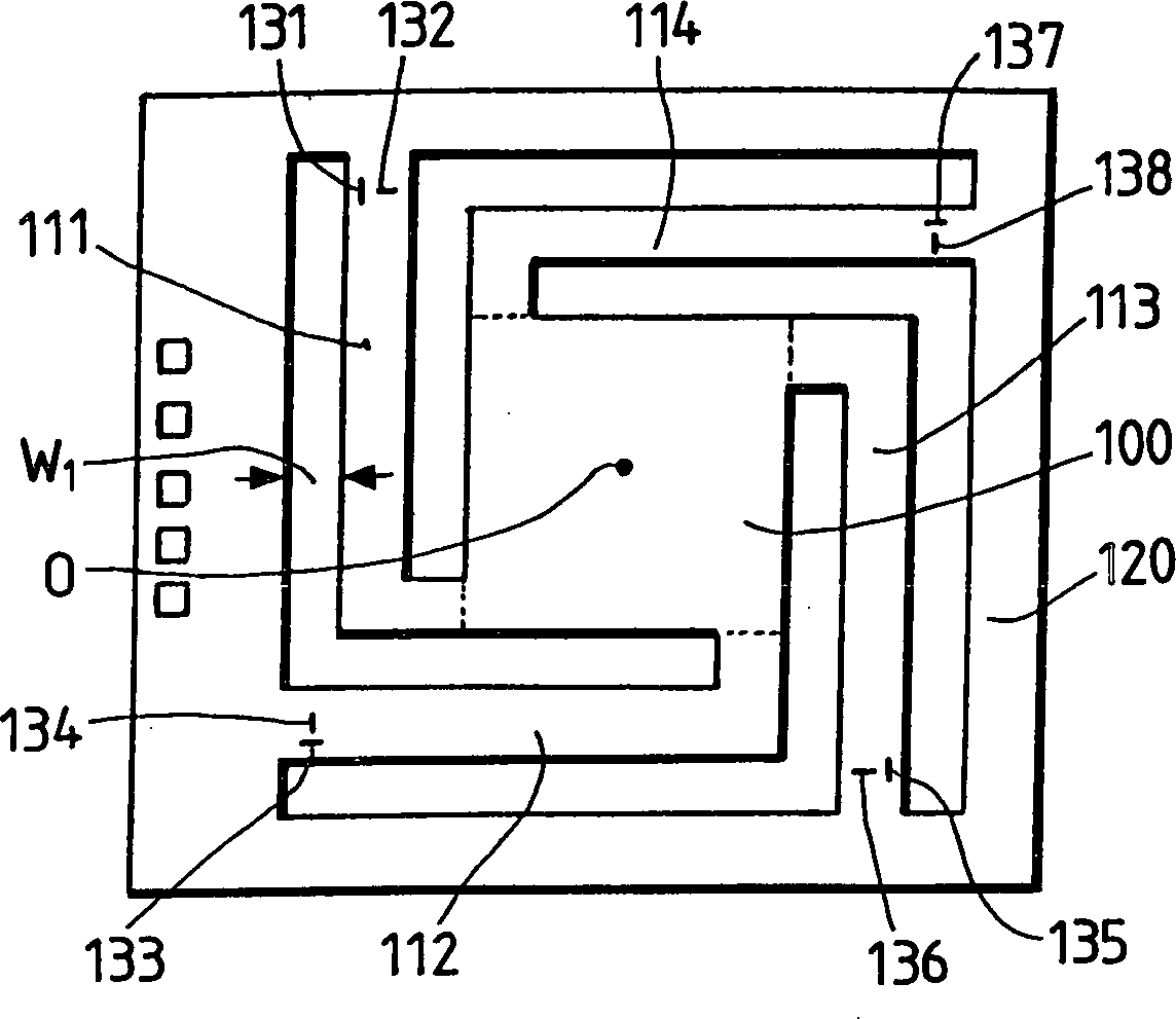
1 zeigt ein erstes Ausführungsbeispiel eines
Halbleiterbeschleunigungssensors. 1A ist eine
Draufsicht, 1B ist ein Querschnitt und 1C ist
ein Schaltkreisdiagramm. In den 1A und 1B umfaßt der Halbleiterbeschleunigungssensor
ein viereckiges, prismaförmiges,
dickes Gewicht 100 aus einem Halbleiter mit einer Dicke
von zum Beispiel 400 μm,
ein dickes Trägerelement 120, das
durch einen vorgegebenen Abstand von dem Gewicht 100 getrennt
ist und so geformt ist, daß es dieses
umgibt, und erste und zweite Sätze
von dünnen,
L-förmigen
Balken, die die äußere Peripherie des
Gewichts 100 mit der inneren Periphe rie des Trägerelements 120 verbinden
und die eine Dicke von zum Beispiel 10 bis 40 μm besitzen. Die ersten und zweiten
Sätze bestehen
jeweils aus einem Balkenpaar 111 und 113 und einem
Balkenpaar 112 und 114. In jedem der Balkensätze sind
die Balken so angeordnet, daß,
wenn einer von ihnen um 180 Grad um den Mittelpunkt O des Gewichts 100 gedreht
wird, dieser Balken mit dem anderen Balken zusammenfällt. Dehnungsmeßstreifen 131 bis 138 sind
auf den oberen Flächen
der Balken geformt. 1 shows a first embodiment of a semiconductor acceleration sensor. 1A is a top view 1B is a cross section and 1C is a circuit diagram. In the 1A and 1B For example, the semiconductor acceleration sensor comprises a square, prism-shaped, thick weight 100 of a semiconductor having a thickness of, for example, 400 μm, a thick support element 120 by a given distance from the weight 100 is separated and shaped so as to surround it, and first and second sets of thin, L-shaped beams, which are the outer periphery of the weight 100 with the inner Periphe theory of the support element 120 connect and have a thickness of, for example, 10 to 40 microns. The first and second sentences each consist of a pair of bars 111 and 113 and a pair of bars 112 and 114 , In each of the beam sets, the beams are arranged so that when one of them is 180 degrees about the center O of the weight 100 is rotated, this bar coincides with the other bar. strain 131 to 138 are formed on the upper surfaces of the beams.
In
dem Halbleiterbeschleunigungssensor wird das Gewicht an zwei gegenüberliegenden
Enden von einem Balkenpaar gehal ten. Wenn eine Beschleunigung in
der transversalen Richtung (die nicht die Beschleunigungsmeßrichtung
ist) auf das Gewicht wirkt, ist die Biegung der Balken sehr viel
geringer als bei einem Sensor, bei dem das Gewicht nur an einem
Ende gehalten wird, so daß der
Betrag einer Störausgabe
verringert und die Stabilität
verbessert wird.In
the semiconductor acceleration sensor, the weight at two opposite
Ends held by a pair of beams. When an acceleration in
the transverse direction (which is not the acceleration measuring direction
is) acting on the weight, the bending of the beams is very much
less than a sensor with only one weight
End is held so that the
Amount of an issue
decreases and stability
is improved.
Die
auf den oberen Flächen
der Balken 111 bis 114 geformten Dehnungsmeßstreifen 131 bis 138 sind
klassifiziert in Dehnungsmeßstreifen 131, 133, 135 und 137 eines
ersten Typs, die jeweils auf den oberen Flächen dieser Balken in der Verbindungsseite
der Balken mit dem Trägerelement 120 in
der longitudinalen Richtung des jeweiligen Balkens geformt sind,
und in Dehnungsmeßstreifen 132, 134, 136 und 138 eines
zweiten Typs, die jeweils auf den oberen Flächen dieser Balken in der Verbindungsseite
der Balken mit dem Trägerelement 120 in
der Querrichtung des jeweiligen Balkens geformt sind. Diese Dehnungsmeßstreifen 131 bis 138 sind,
wie in 1C gezeigt, elektrisch miteinander
verbunden und bilden eine Wheatstone-Brücke, in der die Dehungsmeßstreifen 131 und 135 des
ersten Typs, die jeweils auf dem ersten Satz von Balken 111 und 113 geformt sind,
den Dehnungsmeßstreifen 133 und 137 des ersten
Typs, die jeweils auf dem zweiten Satz von dünnen Balken 112 und 114 geformt
sind, gegenüberliegen,
und die Dehungsmeßstreifen 132 und 136 des
zweiten Typs, die jeweils auf dem ersten Satz von Balken 111 und 113 geformt
sind, den Dehnungsmeßstreifen 134 und 138 des
zweiten Typs, die jeweils auf dem zweiten Satz von dünnen Balken 112 und 114 geformt
sind, gegenüberliegen.
In 1C bezeichnet V einen Spannungsversorgungsanschluß und S1 und S2 bezeichnen
Signalausgabeanschlüsse.The on the upper surfaces of the beams 111 to 114 shaped strain gauges 131 to 138 are classified in strain gauges 131 . 133 . 135 and 137 a first type, each on the upper surfaces of these beams in the connecting side of the beam with the support element 120 are formed in the longitudinal direction of the respective beam, and in strain gauges 132 . 134 . 136 and 138 a second type, each on the upper surfaces of these beams in the connecting side of the beams with the support element 120 are formed in the transverse direction of the respective beam. These strain gauges 131 to 138 are, as in 1C shown electrically interconnected and forming a Wheatstone bridge in which the strain gauges 131 and 135 of the first type, each on the first set of beams 111 and 113 are shaped, the strain gauge 133 and 137 of the first type, each on the second set of thin bars 112 and 114 are shaped, opposite, and the Dehungsmeßstreifen 132 and 136 of the second type, each on the first set of beams 111 and 113 are shaped, the strain gauge 134 and 138 of the second type, each on the second set of thin bars 112 and 114 are shaped, opposite each other. In 1C V denotes a power supply terminal and S 1 and S 2 indicate signal output terminals.
Wenn
eine Beschleunigung in der vertikalen Richtung (welche die Beschleunigungsmeßrichtung ist)
auf das Gewicht 100 wirkt, wirkt auf das Gewicht 100 eine
Kraft in der vertikalen Richtung und die Balken 111, 112, 113 und 114 biegen
sich in der durch einen Pfeil P gezeigten Richtung. Zu diesem Zeitpunkt wirkt
eine Zugspannung auf die oberen Flächen der Balken in der Verbindungsseite
derselben mit dem Trägerelement 120,
so daß der
Widerstand jedes Dehnungsmeßstreifens 131, 133, 135 und 137 des ersten
Typs, die in der longitudinalen Richtung des jeweiligen Balken geformt
sind, zunimmt. Im Gegensatz dazu ändert sich der Widerstand der
Dehungsmeßstreifen 132, 134, 136 und 138 des
zweiten Typs, die in der Querrichtung des jeweiligen Balken geformt sind,
nicht. Dies verursacht, daß ein
Detektionssignal, dessen Wert proportional dem Betrag der Beschleunigung
ist, von den Signalausgabeanschlüssen
S1 und S2 der Wheatstone-Brücke ausgegeben wird.When an acceleration in the vertical direction (which is the acceleration measuring direction) on the weight 100 acts, affects the weight 100 a force in the vertical direction and the bars 111 . 112 . 113 and 114 bend in the direction shown by an arrow P. At this time, a tensile stress acts on the upper surfaces of the beams in the connecting side thereof with the support member 120 so that the resistance of each strain gauge 131 . 133 . 135 and 137 of the first type, which are formed in the longitudinal direction of the respective beam increases. In contrast, the resistance of the strain gauges changes 132 . 134 . 136 and 138 of the second type, which are formed in the transverse direction of the respective beam, not. This causes a detection signal whose value is proportional to the amount of acceleration to be output from the signal output terminals S 1 and S 2 of the Wheatstone bridge.
In
diesem Ausführungsbeispiel
ist die Biegungsmittel punktslinie 13 jedes Balkens um
einen Abstand L von dem Schwerpunkt G des Gewichts 100 getrennt.
Wenn eine Beschleunigung in der transversalen Richtung (die nicht
die Beschleunigungsmeßrichtung
ist) auf das Gewicht 100 wirkt, wirkt ein durch den Abstand
L erzeugtes Drehmoment auf das Gewicht 100 und erzeugt
so eine Druckspannung, die auf die obere Fläche des einen der paarigen
Balken 112 und 114 wirkt (zum Beispiel auf den
Balken 112). Zu diesem Zeitpunkt wirkt eine Zugspannung
auf die obere Fläche
des anderen Balken 114. In der Wheatstone-Brücke ändert sich
daher der Widerstand jeder der Dehnungsmeßstreifen 133 und 137 des
ersten Typs, die jeweils auf diesen Balken geformt sind, derart,
daß sich
die Widerstandsänderungen
einander aufheben. Demzufolge gibt die Wheatstone-Brücke kein
Ausgabesignal aus, mit der Ergebnis, daß der Betrag einer Störausgabe
verringert wird.In this embodiment, the bending means is dot-line 13 each beam by a distance L from the center of gravity G of the weight 100 separated. When an acceleration in the transverse direction (which is not the acceleration measuring direction) on the weight 100 acts, a torque generated by the distance L acts on the weight 100 and thus creates a compressive stress on the upper surface of one of the paired beams 112 and 114 acts (for example on the bar 112 ). At this time, a tensile stress acts on the upper surface of the other beam 114 , In the Wheatstone bridge, therefore, the resistance of each of the strain gauges changes 133 and 137 of the first type, each formed on this beam, such that the resistance changes cancel each other out. As a result, the Wheatstone bridge does not output an output signal, with the result that the amount of spurious output is reduced.
In
dem Ausführungsbeispiel
der 1 ist das dicke Gewicht 100 in
der Draufsicht viereckig. Das Gewicht 100 ist nicht auf
eine viereckige Form beschränkt
und kann eine andere Form besitzen, zum Beispiel eine kreisförmige Form.
Auch wenn oben ein Sensor mit dünnen
Balken in einer L-Form beschrieben wurde, sind die Balken nicht
auf eine L-Form beschränkt
und können
eine andere Form besitzen, zum Beispiel eine I-Form oder eine rechtwinklige
Form.In the embodiment of 1 is the thick weight 100 quadrangular in plan view. The weight 100 is not limited to a quadrangular shape and may have another shape, for example, a circular shape. Although a sensor having thin bars in an L-shape has been described above, the bars are not limited to an L-shape and may have another shape, for example, an I-shape or a rectangular shape.
Zweites AusführungsbeispielSecond embodiment
Ein
zweites Ausführungsbeispiel
eines Halbleiterbeschleunigungssensors wird unter Bezugnahme auf
die 2A und 2B beschrieben,
die ein Verfahren zum Herstellen eines Gewichts, eines Trägerelements
und von Balken aus einem Halbleitersubstrat zeigen. 2A ist
eine Draufsicht des Halbleitersubstrats und 2B ist
eine Druntersicht des Halbleitersubstrats.A second embodiment of a semiconductor acceleration sensor will be described with reference to FIGS 2A and 2 B which teaches a method of manufacturing a weight, a support member, and beams from a semiconductor substrate. 2A is a plan view of the semiconductor substrate and 2 B is a bottom view of the semiconductor substrate.
Bei
dem in 2 gezeigten Verfahren werden
ein Gewicht 100, ein Trägerelement 120 und
Balken 111, 112, 113 und 114 wie
folgt hergestellt. Zunächst
werden, wie in 2A gezeigt, Bereiche, die schraffiert
und mit 210 bezeichnet sind, zum Beispiel durch einen Plasmaätzprozeß von der
oberen Fläche des
Halbleitersubstrats bis zu einer Tiefe gleich oder größer als
die Dicke des Gewichts 100 geätzt. Danach werden Bereiche,
die in 2B schraffiert und mit 211 be
zeichnet sind, so geätzt,
daß sie
die Balken 111, 112, 113 und 114 mit
einer Dicke von zum Beispiel 10 bis 40 μm bilden.At the in 2 shown methods become a weight 100 , a carrier element 120 and beams 111 . 112 . 113 and 114 prepared as follows. First, as in 2A shown areas hatched and with 210 are designated, for example, by a plasma etching process from the upper surface of the semiconductor substrate to a depth equal to or greater than the thickness of the weight 100 etched. After that, areas that are in 2 B hatched and with 211 be etched so etched that they are the beams 111 . 112 . 113 and 114 with a thickness of, for example, 10 to 40 microns.
In
der Erfindung ist jede der Arbeitsbreiten W1 und
W2 der geätzten Bereiche 210 und 211,
die jeweils von den oberen und unteren Flächen des Halbleitersubstrats
geätzt
werden, entlang der gesamten Länge
konstant. Daher findet der Ätzprozeß mit einer konstanten
Rate statt, was zu einer verbesserten Arbeitsgenauigkeit führt.In the invention, each of the working widths W 1 and W 2 is the etched area 210 and 211 respectively etched from the upper and lower surfaces of the semiconductor substrate, are constant along the entire length. Therefore, the etching process takes place at a constant rate, resulting in improved working accuracy.
Drittes AusführungsbeispielThird embodiment
Die 3A und
B zeigen ein drittes Ausführungsbeispiel
eines Halbleiterbeschleunigungssensors. Das Ausführungsbeispiel der 3A und 3B ist
auf die gleiche Weise ausgeführt
wie das der 2, außer daß dünne Balken 111, 112, 113 und 114 mit
einer I-förmigen
Form oder einer rechtwinkligen Form anstelle der in 2 verwendeten L-förmigen Form
vorgesehen sind und daß diese
Balken so angeordnet sind, daß,
wenn die Balken 111 und 112 um 180 Grad um den
Mittelpunkt O des Gewichts 100 gedreht werden, diese Balken
jeweils mit den Balken 113 und 114 zusammenfallen
und daß die
Balken 111 und 112 mit den Balken 114 und 113 jeweils
symmetrisch bezüglich
der longitudinalen Achse V des Gewichts 100 sind.The 3A and B show a third embodiment of a semiconductor acceleration sensor. The embodiment of 3A and 3B is executed in the same way as the 2 except that thin bars 111, 112 . 113 and 114 with an I-shaped shape or a rectangular shape instead of in 2 used L-shaped form are provided and that these beams are arranged so that when the beams 111 and 112 180 degrees around the center O of the weight 100 be rotated, these bars each with the bars 113 and 114 coincide and that the bars 111 and 112 with the bars 114 and 113 each symmetrical with respect to the longitudinal axis V of the weight 100 are.
Viertes AusführungsbeispielFourth embodiment
Die 4 und 5 zeigen ein viertes Ausführungsbeispiel
eines Halbleiterbeschleunigungssensors. 4 ist ein
Querschnitt, und 5 zeigt den Sensor
der 4 in größerem Detail. 5A ist
ein Draufsicht eines Sensorbereichs, der ein Gewicht 100,
ein Trägerelement 120 und
Balken 111 bis 114 umfaßt, und 5B ist
eine Druntersicht eines Trägersubstrats 450.
In dem Ausführungsbeispiel
der 4 und 5 ist eine
Mehrzahl von Signalanschlüssen 430 auf
einer Seite, die mit auf den oberen Flächen der Balken geformten Dehnungsmeßstreifen
verbunden sind, und eine Mehrzahl von Blind-Signalanschlüssen 431 auf
der einen Seite, die dieselbe Form wie die Signalanschlüsse 430 besitzen,
in der Peripherie der oberen Fläche
des Trägerelements 120 in im
wesentlichen gleichen Abständen
angeordnet. Das Trägersubstrat 450 ist
mit einer Mehrzahl von Signalanschlüssen 432 und Blind-Signalanschlüssen 433 der
anderen Seite versehen, die jeweils der Mehrzahl von Signalanschlüssen 430 und
Blindsignalanschlüssen 431 der
einen Seite gegenüberliegen und
mit diesen verbunden sind. Die auf den Balken geformten Dehnungsmeßstreifen
sind über
die Signalanschlüsse 432 der
anderen Seite und mit den Signalanschlüssen verbundenen Verbindungsanschlüssen 460 mit
einer externen Einheit verbunden. Die Summe der Höhe der Signalanschlüsse 430 auf der
einen Seite und der Signalanschlüsse 432 auf
der anderen Seite sowie die Summe der Höhe der Blind-Signalanschlüsse 431 auf
der einen Seite und der Blind-Signalanschlüsse 433 auf der anderen
Seite sind auf einen Wert H1 eingestellt,
der geringfügig größer ist
(zum Beispiel 10 bis 30 μm)
als der Verschiebebetrag des Gewichts 100 während des
Betriebs. Wenn also ein Stoß auf
den Halbleiterbeschleunigungssensor wirkt, wird das Gas zwischen der
oberen Fläche
des Gewichts 100 und der unteren Fläche des Trägersubstrats 450 komprimiert,
so daß ein
Dämpfungsvorgang
im Hochfrequenzbereich von zum Beispiel 500 Hz oder höher für das Gewicht 100 durchgeführt wird,
wodurch die Stoßfestigkeit
des Sensors verbessert wird.The 4 and 5 show a fourth embodiment of a semiconductor acceleration sensor. 4 is a cross section, and 5 shows the sensor the 4 in greater detail. 5A FIG. 10 is a top view of a sensor area that is a weight. FIG 100 , a carrier element 120 and beams 111 to 114 includes, and 5B is a bottom view of a carrier substrate 450 , In the embodiment of 4 and 5 is a plurality of signal terminals 430 on a side connected to strain gauges formed on the upper surfaces of the beams, and a plurality of dummy signal terminals 431 on the one hand, the same shape as the signal connectors 430 own, in the periphery of the upper surface of the support element 120 arranged at substantially equal intervals. The carrier substrate 450 is with a plurality of signal terminals 432 and blind signal terminals 433 the other side, each of the plurality of signal terminals 430 and dummy signal terminals 431 one side opposite and connected to these. The strain gauges formed on the beam are across the signal terminals 432 the other side and connection terminals connected to the signal terminals 460 connected to an external unit. The sum of the height of the signal connections 430 on one side and the signal connections 432 on the other side as well as the sum of the height of the dummy signal connections 431 on one side and the dummy signal connections 433 on the other hand, are set to a value H 1 which is slightly larger (for example, 10 to 30 μm) than the amount of shift of the weight 100 during operation. Thus, when a shock acts on the semiconductor acceleration sensor, the gas between the upper surface of the weight 100 and the lower surface of the support substrate 450 compressed, so that a damping operation in the high frequency range of, for example 500 Hz or higher for the weight 100 is performed, whereby the shock resistance of the sensor is improved.
Es
ist günstig,
die Signalanschlüsse 430 und 432 und
die Blind-Signalanschlüsse 431 und 433 der einen
und der anderen Seite aus einem Dickfilm aus einem Metall oder einer
Legierung wie etwa aus Au, Ag oder Pb/Sn herzustellen.It is convenient, the signal connections 430 and 432 and the dummy signal terminals 431 and 433 one and the other side of a thick film of a metal or an alloy such as Au, Ag or Pb / Sn produce.
Fünftes AusführungsbeispielFifth embodiment
Die 6A und 6B zeigen
ein fünftes Ausführungsbeispiel
eines Halbleiterbeschleunigungssensors. 6A ist
ein Querschnitt, der den Fall zeigt, wo ein Stoß auf den Sensor der 6A wirkt.
In 6A ist ein zusätzliches
Gewichts- und Stoppelement 520 mit einer umgekehrten konvexen Form
auf der oberen Fläche
des Gewichts 100 angeordnet. Die äußere Peripherie des zusätzlichen
Gewicht- und Stoppelements 520 ist größer als die innere Peripherie
des Trägerelements 120.
Der Abstand H2 zwischen der unteren Fläche des äußeren peripheren
Bereichs des zusätzlichen
Gewicht- und Stoppelements 520 und die obere Fläche des
Trägerelements 120 ist
auf einen Wert eingestellt, der kleiner ist als der erlaubte Verschiebungsbetrag
des Gewichts 100. Wenn daher ein Stoß, zum Beispiel ein Stoß mit einer
geringen Frequenz von einigen zehn Hz oder weniger, auf den Halbleiterbeschleunigungssensor
wirkt, wird die Biegung des Gewichtes 100 innerhalb der
erlaubten Verschiebung durch das zusätzliche Gewicht- und Stoppelement 520 eingeschränkt, wie
in 6B gezeigt. Das Vorhandensein des zusätzlichen
Gewicht- und Stoppelements 520 erhöht das Gewicht des Ge wichts.
Dies trägt
zu einer Verbesserung der Empfindlichkeit des Sensors bei.The 6A and 6B show a fifth embodiment of a semiconductor acceleration sensor. 6A is a cross section showing the case where a shock to the sensor 6A acts. In 6A is an additional weight and stop element 520 with an inverted convex shape on the upper surface of the weight 100 arranged. The outer periphery of the additional weight and stop element 520 is larger than the inner periphery of the support member 120 , The distance H 2 between the lower surface of the outer peripheral portion of the additional weight and stopper member 520 and the upper surface of the support member 120 is set to a value smaller than the allowable shift amount of the weight 100 , Therefore, when a shock, for example, a shock of a few tens Hz or less, acts on the semiconductor acceleration sensor, the bending of the weight becomes 100 within the permitted displacement by the additional weight and stop element 520 restricted, as in 6B shown. The presence of additional weight and stop elements 520 increases the weight of the weight. This contributes to an improvement in the sensitivity of the sensor.
Sechstes AusführungsbeispielSixth embodiment
Die 6A und 6B zeigen
auch ein sechstes Ausführungsbeispiel
eines Halbleiterbeschleunigungssensors. In 6A ist
ein Trägersubstrat 510 mit
einer sich nach oben öffnenden
Vertiefung 511 auf der unteren Fläche des Trägerelements 120 angeordnet.
Die Vertiefung 511 ist größer als die äußere Peripherie
des Gewichts 100. Der Abstand H1 zwischen
der Fläche
der Vertiefung 511 und der unteren Fläche des Gewichts 100 ist
auf einen Wert eingestellt, der geringfügig größer ist (zum Beispiel um 10
bis 30 μm)
als der bewegliche Verschiebebetrag des Gewichts 100 während des
Betriebs. Wenn also ein Stoß auf
den Halbleiterbeschleunigungssensor wirkt, wird das Gas zwischen
der unteren Fläche
des Gewichts 100 und der Fläche der Vertiefung 511 des Trägersubstrats 510 komprimiert,
so daß ein
Dämpfungsvorgang
auf dieselbe Weise wie in dem Ausführungsbeispiel der 4 auf
das Gewicht wirkt, wodurch die Stoßfestigkeit des Sensors verbessert
wird.The 6A and 6B also show a sixth embodiment of a semiconductor acceleration sensor. In 6A is a carrier substrate 510 with an upwardly opening depression 511 on the lower surface of the carrier element 120 arranged. The depression 511 is greater than the outer periphery of the weight 100 , The distance H 1 between the surface of the recess 511 and the lower surface of the weight 100 is set to a value slightly larger (for example, 10 to 30 μm) than the movable amount of shift of the weight 100 during operation. Thus, when a shock acts on the semiconductor acceleration sensor, the gas between the lower surface of the weight 100 and the surface of the recess 511 of the carrier substrate 510 compressed, so that a damping operation in the same manner as in the embodiment of 4 acting on the weight, whereby the shock resistance of the sensor is improved.
Siebtes AusführungsbeispielSeventh embodiment
Die 7 und 8A bis 8C zeigen
ein siebtes Ausführungsbeispiel
eines Halbleiterbeschleunigungssensors. 7 ist ein
Querschnitt, und die 8A bis 8C zeigen
den Sensor der 7 in größerem Detail. 8A ist
eine Druntersicht eines oberen Trägersubstrats 610, 8B ist
eine Draufsicht eines Sensorbereichs mit einem Gewicht 100,
einem Trägerelement 120 und
Balken 111 bis 114, und 8C ist
eine Draufsicht eines unteren Trägersubstrats 620.
In den 7 und 8 sind das obere
Trägersubstrat 610 und
das untere Trägersubstrat 620 jeweils
auf der oberen und der unteren Fläche des Trägerelements 120 angeordnet.
Das obere Trägersubstrat 610 besitzt
eine sich nach unten öffnende
Vertiefung 611. Die Vertiefung 611 ist größer als
die äußere Peripherie
des Gewichts 100. In der Vertiefung 611 ist eine
Mehrzahl (z.B. 4) von nach unten gehen Ausstülpungen 612 an der äußeren Peripherie
des Gewichts 100 gegenüberliegenden
Stellen geformt. Das untere Trägersubstrat 620 besitzt eine
sich nach oben öffnende
Vertiefung 621. Die Vertiefung 621 ist größer als
die äußere Peripherie des
Gewichts 100. In der Vertiefung 621 ist eine Mehrzahl
(z.B. 4) von nach oben gehenden Ausstülpungen 622 an der äußeren Peripherie
des Gewichts 100 gegenüberliegenden
Stellen geformt. Die Abstände
zwischen den oberen und unteren Flächen des Gewichts 100 und
den Flächen
der Vertiefungen 611 und 621 der oberen und unteren
Trägersubstrate 610 und 620 sind
auf einen Wert H1 eingestellt, der geringfügig größer ist
(zum Beispiel um 10 bis 40 μm) als
der bewegliche Verschiebebetrag des Gewichts 100 während des
Betriebs. Die Abstände
zwischen den oberen und unteren Flächen des Gewichts 100 und
den in den Vertiefungen 611 und 621 geformten Ausstülpungen 612 und 622 der
oberen und unteren Trägersub strate 610 und 620 sind
auf einen Wert H2 eingestellt, der kleiner
ist als der erlaubte Verschiebebetrag des Gewichts 100.The 7 and 8A to 8C show a seventh embodiment of a semiconductor acceleration sensor. 7 is a cross section, and the 8A to 8C show the sensor the 7 in greater detail. 8A is a bottom view of an upper carrier substrate 610 . 8B Figure 11 is a plan view of a sensor area with a weight 100 , a support element 120 and beams 111 to 114 , and 8C is a plan view of a lower carrier substrate 620 , In the 7 and 8th are the upper carrier substrate 610 and the lower carrier substrate 620 respectively on the upper and lower surfaces of the support member 120 arranged. The upper carrier substrate 610 has a downwardly opening recess 611 , The depression 611 is greater than the outer periphery of the weight 100 , In the depression 611 is a plurality (eg 4) of go down bulges 612 on the outer periphery of the weight 100 shaped opposite places. The lower carrier substrate 620 has an upwardly opening recess 621 , The depression 621 is greater than the outer periphery of the weight 100 , In the depression 621 is a plurality (eg 4) of upwardly projecting protuberances 622 on the outer periphery of the weight 100 shaped opposite places. The distances between the upper and lower surfaces of the weight 100 and the areas of the depressions 611 and 621 the upper and lower carrier substrates 610 and 620 are set to a value H 1 which is slightly larger (for example, 10 to 40 μm) than the movable amount of shift of the weight 100 during operation. The distances between the upper and lower surfaces of the weight 100 and in the wells 611 and 621 shaped protuberances 612 and 622 the upper and lower Trägerub strate 610 and 620 are set to a value H 2 which is smaller than the allowable shift amount of the weight 100 ,
Wenn
also ein Stoß auf
den Halbleiterbeschleunigungssensor wirkt, wird das Gas zwischen der
oberen und unteren Fläche
des Gewichts 100 und der Fläche der Vertiefung 611 des
oberen Trägersubstrats 610 oder
die Fläche
der Vertiefung 621 des unteren Trägersubstrats 620 komprimiert,
so daß ein
Dämpfungsvorgang
auf dieselbe Weise wie in dem vierten Ausführungsbeispiel der 4 und 5 auf das Gewicht wirkt, wodurch die Stoßfestigkeit
des Sensors verbessert wird. Darüberhinaus
wird die Biegung des Gewichts 100 durch die in den Vertiefungen 611 oder 621 der
oberen oder unteren Trägersubstrate 610 oder 620 geformten
Ausstülpungen 612 oder 622 auf
dieselbe Weise wie bei dem fünften,
in 6 gezeigten Ausführungsbeispiel
innerhalb des erlaubten Verschiebebetrags eingeschränkt.Thus, when a shock acts on the semiconductor acceleration sensor, the gas between the upper and lower surfaces of the weight 100 and the surface of the recess 611 of the upper carrier substrate 610 or the area of the depression 621 of the lower carrier substrate 620 compressed, so that a damping operation in the same manner as in the fourth embodiment of 4 and 5 acting on the weight, whereby the shock resistance of the sensor is improved. In addition, the bending of the weight 100 through the in the wells 611 or 621 the upper or lower carrier substrates 610 or 620 shaped protuberances 612 or 622 in the same way as in the fifth, in 6 shown embodiment limited within the allowable shift amount.
Achtes AusführungsbeispielEighth embodiment
Die 9 und 10A bis 10C zeigen ein
achtes Ausführungsbeispiel
eines Halbleiterbeschleunigungssensors. 9 ist ein
Querschnitt, und die 10A bis 10C zeigen
den Sensor der 9 in größerem Detail. 10A ist eine Druntersicht eines oberen Trägersubstrats 710, 10B ist eine Draufsicht eines Sensorbereichs mit
einem Gewicht 100, einem Trägerelement 120 und
Balken 111 bis 114, und 10C ist eine
Draufsicht eines unteren Trägersubstrats 720.The 9 and 10A to 10C show an eighth embodiment of a semiconductor acceleration sensor. 9 is a cross section, and the 10A to 10C show the sensor the 9 in greater detail. 10A is a bottom view of an upper carrier substrate 710 . 10B Figure 11 is a plan view of a sensor area with a weight 100 , a support element 120 and beams 111 to 114 , and 10C is a plan view of a lower carrier substrate 720 ,
Die
Konfiguration und die Arbeitsweise des in den 9 und 10 gezeigten achten Ausführungsbeispiels
sind die gleichen wie bei dem in den 7 und 8 gezeigten siebten Ausführungsbeispiel,
außer daß Ausstülpungen 712 und 722 an
der äußeren Peripherie
des Gewichtes 100 gegenüberliegenden Stellen
anstelle der in den 7 und 8 gezeigten Mehrzahl
(z.B. 4) von Ausstülpungen 612 und 622, die
an der äußeren Peripherie
des Gewichtes 100 gegenüberliegenden
Stellen geformt sind, angeordnet sind. Die Ausstülpungen 712 und 722 erstrecken
sich entlang der äußeren Peripherie
des Gewichtes 100.The configuration and operation of the in the 9 and 10 eighth embodiment shown are the same as in the 7 and 8th shown seventh embodiment, except that protuberances 712 and 722 on the outer periphery of the weight 100 opposite places instead of in the 7 and 8th shown plurality (eg 4) of protuberances 612 and 622 attached to the outer periphery of the weight 100 are formed opposite positions are arranged. The protuberances 712 and 722 extend along the outer periphery of the weight 100 ,
Wie
in 11 gezeigt, ist, falls erforderlich, jeder der
oben beschriebenen Halbleiterbeschleunigungssensoren in einem hermetisch
abgeschlossenen Behälter 850 untergebracht,
der ein inertes Gas enthält.
Diese Anordnung ermöglicht,
die Sensoren hinreichend sicher auch unter harten Umweltbedingungen
für Kraftfahrzeugsensoren
zu verwenden. In 11 bezeichnet 810 einen
der Halbleiterbeschleunigungssensoren, und 820 bezeichnet
einen Verstärker
für ein
Detektionssignal.As in 11 is shown, if necessary, each of the above-described semiconductor acceleration sensors in a hermetically sealed container 850 housed, which contains an inert gas. This arrangement makes it possible to use the sensors with sufficient reliability even under harsh environmental conditions for motor vehicle sensors. In 11 designated 810 one of the semiconductor acceleration sensors, and 820 denotes an amplifier for a detection signal.
Die 17A und 17B zeigen
einen Halbleiterbeschleunigungssensor. 17A ist
eine Draufsicht und 17B ist ein Querschnitt entlang der
Linie A-A der 17A. Wie in den 17A und 17B gezeigt,
ist der Halbleiterbeschleunigungssensor aus einem Halbleiter geformt
und umfaßt
ein quadratisches, dickwandiges Gewicht 901, das zum Beispiel
400 μm dick
ist, einen dickwandigen Träger 906,
der mit einer inneren quadratischen Öffnung versehen ist, die in
einem vorgegebenen Abstand von dem Gewicht 901 angeordnet
ist und die so geformt ist, daß sie
das Gewicht 901 umgibt, vier dünnwandige Balken 902, 903, 904, 905,
die zum Beispiel 20–40 μm dick sind
zum Verbinden von vier Endseiten auf beiden gegenüberliegenden, äußeren Seiten des
Gewichts 901 mit den jeweils gegenüberliegenden, inneren Seiten
des Trägers 906,
und jeweils in den Balken 902, 903, 904, 905 geformte
Dehnungsmeßstreifen 902A, 902B, 903A, 903B, 904A, 904B, 905A, 905B.
Die Dehnungsmeßstreifen 902A, 903A, 904A, 905A von
all diesen Dehnungsmeßstreifen sind
in den oberen Oberflächen
der Verbindungen zwischen dem Träger 906 und
den Balken 902, 903, 904, 905 jeweils
in der Längsrichtung
der Balken geformt. Auf der anderen Seite sind die Dehnungsmeßstreifen 902B, 903B, 904B, 905B in
den oberen Oberflächen
der Verbindungen zwischen dem Gewicht 901 und den Balken 902, 903, 904, 905 jeweils in
der Längsrichtung
der Balken geformt. Unter der Annahme, daß die in den oberen Oberflächen der Verbindungen
zwischen den Balken und dem Träger geformten
Dehnungsmeßstreifen 902A, 903A, 904A, 905A Dehnungsmeßstreifen
der ersten Seite genannt werden und daß die in den oberen Oberflächen der
Verbindungen zwischen den Balken und dem Gewicht geformten Dehnungsmeßstreifen 902B, 903B, 904B, 905B Dehnungsmeßstreifen
der zweiten Seite genannt werden, kann eine Wheatstone-Brücke, wie in 19 gezeigt
gebildet werden, indem zwei Dehnungs meßstreifen 902A, 905A der
vier Dehnungsmeßstreifen
den Dehnungsmeßstreifen 903A, 904A symmetrisch
bezüglich
dem Mittelpunkt C des Gewichts 901 gegenüberliegen
und indem zwei Dehnungsmeßstreifen 902B, 905B der
vier Dehnungsmeßstreifen
den Dehnungsmeßstreifen 903B, 904B symmetrisch
bezüglich
dem Mittelpunkt C des Gewichts 901 gegenüberliegen.
In diesem Fall bezeichnet V einen Spannungsversorgungsanschluß, G einen
Masseanschluß und
S1, S2 Signalausgabeanschlüsse.The 17A and 17B show a semiconductor acceleration sensor. 17A is a top view and 17B is a cross section along the line AA of 17A , As in the 17A and 17B As shown, the semiconductor acceleration sensor is formed of a semiconductor and has a square, thick-walled weight 901 which is, for example, 400 μm thick, a thick-walled carrier 906 which is provided with an inner square opening which is a predetermined distance from the weight 901 is arranged and which is shaped so that the weight 901 surrounds, four thin-walled beams 902 . 903 . 904 . 905 which are, for example, 20-40 μm thick for joining four end sides on both opposite, outer sides of the weight 901 with the respective opposite, inner sides of the carrier 906 , and in each case in the bars 902 . 903 . 904 . 905 shaped strain gauges 902A . 902B . 903A . 903B . 904A . 904B . 905A . 905B , The strain gauges 902A . 903A . 904A . 905A Of all these strain gauges are in the upper surfaces of the connections between the carrier 906 and the beam 902 . 903 . 904 . 905 each formed in the longitudinal direction of the beam. On the other side are the strain gauges 902B . 903B . 904B . 905B in the upper surfaces of the connections between the weight 901 and the beam 902 . 903 . 904 . 905 each formed in the longitudinal direction of the beam. Assuming that the strain gauges formed in the upper surfaces of the joints between the beams and the beam 902A . 903A . 904A . 905A Called strain gauges of the first side and that in the upper surfaces of the joints between the bars and the weight formed strain gauges 902B . 903B . 904B . 905B Strain gauges can be called the second side, a Wheatstone bridge, as in 19 shown formed by two strain gauges 902A . 905A the four strain gauges the strain gauges 903A . 904A symmetrical with respect to the center C of the weight 901 opposite and by two strain gauges 902B . 905B the four strain gauges the strain gauges 903B . 904B symmetrical with respect to the center C of the weight 901 are opposite. In this case, V denotes a power supply terminal, G a ground terminal, and S1, S2 signal output terminals.
Wenn
eine Beschleunigung in Richtung des Pfeiles V in 17B auf das Gewicht 901 wirkt, also in
einer Richtung senkrecht zum Gewicht 901 (die Richtung,
in der die Beschleunigung gemessen wird), erfährt das Gewicht 901 eine
vertikale Kraft Fv, bewegt sich nach unten, wie in 20 gezeigt,
und wird von den Balken 902, 903 und 904, 905 auf
beiden Seiten gehalten. Zu diesem Zeitpunkt wirkt eine Zugspannung
auf die oberen Oberflächen
der Verbindungen zwischen den Balken und dem Träger 906, während Druckspannungen
auf die oberen Oberflächen der
Verbindungen zwischen den Balken und dem Gewicht 901 wirken.
Dann nehmen die Widerstände
der Dehnungsmeßstreifen 902A, 903A, 904A, 905A auf der
ersten Seite zu und die Widerstände
der Dehnungsmeßstreifen 902B, 903B, 904B, 905B auf
der zweiten Seite nehmen ab. Meßsignale,
deren Höhe proportional
der Beschleunigung ist, werden folglich von den Ausgabeanschlüssen S1,
S2 der Wheatstone-Brücke
ausgegeben.When an acceleration in the direction of the arrow V in 17B on the weight 901 acts, so in a direction perpendicular to the weight 901 (the direction in which the acceleration is measured) experiences the weight 901 a vertical force Fv, moves down, as in 20 shown, and is from the bars 902 . 903 and 904 . 905 held on both sides. At this time, a tensile stress acts on the upper surfaces of the joints between the beams and the beam 906 while compressive stresses on the upper surfaces of the joints between the beams and the weight 901 Act. Then take the resistors of the strain gauges 902A . 903A . 904A . 905A on the first page and the resistances of the strain gauges 902B . 903B . 904B . 905B on the second page decrease. Measurement signals whose magnitude is proportional to the acceleration are consequently output from the output terminals S1, S2 of the Wheatstone bridge.
Wenn
eine Beschleunigung in der Richtung des Pfeiles H in 17B auf das Gewichts 901 wirkt, also
in der Querrichtung (die Richtung, in der die Beschleunigung nicht
ge messen wird), erzeugt ein Drehmoment, das durch den Abstand L
von der Spannungsmittelpunktslinie 909 des Balkens zum Schwerpunkt
W des Gewichts 901 und die in dem Gewichts 901 aufgrund
der Beschleunigung erzeugte Querkraft Fh erzeugt wird, eine Verbiegung
wie in 21 gezeigt. Hinsichtlich der
Balken 902, 903 auf der Seite, die von dem Gewicht 901 gedrückt wird, wirkt
eine Druckspannung auf die obere Oberfläche der Verbindung jedes Balkens
mit dem Träger
und eine Zugspannung wirkt auf die obere Oberfläche der Verbindung jedes Balkens
mit dem Gewicht. Hinsichtlich der Balken 904, 905 auf
der Seite, die von dem Gewicht 901 gezogen wird, wirkt
eine Zugspannung auf die obere Oberfläche der Verbindung jedes Balkens
mit dem Träger
und eine Druckspannung wirkt auf die obere Oberfläche der
Verbindung jedes Balkens mit dem Gewicht.When an acceleration in the direction of the arrow H in 17B on the weight 901 acts, ie in the transverse direction (the direction in which the acceleration is not measured ge), generates a torque by the distance L from the tension center line 909 of the beam to the center of gravity W of the weight 901 and in the weight 901 generated due to the acceleration generated lateral force Fh, a deflection as in 21 shown. Regarding the bars 902 . 903 on the side, by the weight 901 is pressed, a compressive stress acts on the upper surface of the connection of each beam with the carrier and a tensile stress acts on the upper surface of the connection of each beam with the weight. Regarding the bars 904 . 905 on the side, by the weight 901 is pulled, a tensile stress acts on the upper surface of the connection of each beam to the carrier and a compressive stress acts on the upper surface of the connection of each beam to the weight.
Daher
ergeben die beiden Paare von Dehnungsmeßstreifen 902A, 905A und 903A, 904A,
die symmetrisch bezüglich
des Mittelpunktes C des Gewichtes 901 unter den vier Dehnungsmeßstreifen 902A, 903A, 904A, 905A auf
der ersten Seite sind, die folgenden Ergebnisse: der Widerstand
von 902A nimmt ab und der von 905A nimmt zu, so
daß sich
die Widerstandsänderungen
aufheben; und der Widerstand von 903A nimmt ab und der
von 904A nimmt zu, so daß sich die Widerstandsänderungen
ebenfalls aufheben. Dies ist ebenfalls der Fall bei den Dehnungsmeßstreifen 902B, 903B, 904B, 905B der zweiten
Seite, deren Widerstandsänderungen
sich aufheben. Mit anderen Worten, es wird kein Signal von der Wheatstone-Brücke ausgegeben.Therefore, the two pairs of strain gauges 902A . 905A and 903A . 904A which are symmetrical with respect to the center C of the weight 901 under the four strain gauges 902A . 903A . 904A . 905A on the first page are, the following results: the resistance of 902A decreases and that of 905A increases, so that the resistance changes cancel; and the resistance of 903A decreases and that of 904A increases, so that the resistance changes also cancel. This is also the case with the strain gauges 902B . 903B . 904B . 905B the second side whose resistance changes cancel each other out. In other words, no signal is output from the Wheatstone bridge.
Da
das Gewicht 901 dieses Halbleiterbeschleunigungssensors
von den Balken 902, 903 und 904, 905 auf
beiden Seiten gehalten wird, wird das Gewicht von den Balken auf
der linken und der rechten Seite gehalten, wenn eine Beschleunigung
in der Querrichtung (die nicht die Meßrichtung ist) wirkt. Daher
ist die Biegung der Balken ist in diesem Fall viel geringer als
die der Balken im herkömmlichen
Fall, bei dem das Gewicht nur von den Balken auf einer Seite gehalten
wird. Weiterhin wird die Störausgabe deutlich
verringert, da sich die Widerstandsänderungen der Dehnungsmeßstreifen
gegenseitig aufheben, wie zuvor erklärt.Because the weight 901 this semiconductor acceleration sensor from the beams 902 . 903 and 904 . 905 is held on both sides, the weight is held by the beams on the left and right sides when acceleration in the transverse direction (which is not the measuring direction) acts. Therefore, the bending of the beams in this case is much lower than that of the beams in the conventional case, in which the weight is held only by the beams on one side. Furthermore, the spurious output is significantly reduced as the resistance changes of the strain gauges cancel each other out, as previously explained.
Die 18A und 18B zeigen
einen weiteren Halbleiterbeschleunigungssensor entsprechend der
vorliegenden Erfindung: 18A ist
eine Draufsicht, und 18B ist ein Querschnitt entlang der
Linie B-B der 18A. Wie in den 18A und 18B gezeigt,
ist der Halbleiterbeschleunigungssensor aus einem Halbleiter geformt
und umfaßt
ein Gewicht 901 mit einem quadratischen, dickwandigen,
zentralen Bereich 901A, der zum Beispiel 400 μm dick ist,
und vier quadratische, dickwandige Ausstülpungen 901A, 901B, 901C, 901D,
die auf den jeweiligen Seiten des zentralen Bereichs 901A geformt sind,
wobei die Seiten davon untereinander einen rechten Winkel um den
Mittelpunkt des zentralen Bereichs 901A bilden, einen dickwandigen
Träger 906 mit
einer quadratischen, inneren Öffnung,
die in einem vorgegebenen Abstand von den äußeren Seiten der Ausstülpungen 901A, 901B, 901C, 901D des
Gewichts 901 entfernt derart angeordnet ist, daß sie das Gewicht 901 umgibt,
vier dünnwandige
Balken 902, 903, 904, 905, die
zum Beispiel 20–40 μm dick sind, zum
Verbinden der einen Seiten der Ausstülpungen 901A, 901B, 901C, 901D des
Gewichts 901, wobei die Seiten davon untereinander einen
rechten Winkel um den Mittelpunkt des zentralen Bereichs 901A des Gewichts 901 bilden,
mit den jeweils gegenüberliegenden
Seiten des Trägers 906 und
in den jeweiligen Balken 902, 903, 904, 905 geformte
Dehnungsmeßstreifen 902A, 902B, 903A, 903B, 904A, 904B, 905A, 905B.
Die Dehnungsmeßstreifen 902A, 903A, 904A, 905A von
all diesen Dehnungsmeßstreifen sind
in den oberen Oberflächen
der Verbindungen zwischen dem Träger 906 und
den Balken 902, 903, 904, 905 jeweils
in der Längsrichtung
der Balken geformt. Auf der anderen Seite sind die Dehnungsmeßstreifen 902B, 903B, 904B, 905B von
all diesen Dehnungsmeßstreifen
in den oberen Oberflächen
der Verbindungen zwischen dem Gewicht 901 und den Balken 902, 903, 904, 905 jeweils
in der Längsrichtung
der Balken geformt. Die Dehnungsmeßstreifen sind genauso angeordnet,
wie in den 17A und 17B gezeigt.The 18A and 18B show a further semiconductor acceleration sensor according to the present invention: 18A is a top view, and 18B is a cross section along the line BB of 18A , As in the 18A and 18B As shown, the semiconductor acceleration sensor is formed of a semiconductor and includes a weight 901 with a square, thick-walled, central area 901A which is, for example, 400 μm thick, and four square, thick-walled protuberances 901A . 901B . 901C . 901D on the respective pages of the central area 901A are formed with the sides thereof at right angles to each other about the center of the central area 901A form a thick-walled carrier 906 with a square, inner opening that is at a predetermined distance from the outer sides of the protuberances 901A . 901B . 901C . 901D of weight 901 away is arranged so that they the weight 901 surrounds, four thin-walled beams 902 . 903 . 904 . 905 , which are for example 20-40 microns thick, for connecting the one side of the protuberances 901A . 901B . 901C . 901D of weight 901 the sides of which are at right angles to each other about the center of the central area 901A of weight 901 form, with the opposite sides of the carrier 906 and in the respective bars 902 . 903 . 904 . 905 shaped strain gauges 902A . 902B . 903A . 903B . 904A . 904B . 905A . 905B , The strain gauges 902A . 903A . 904A . 905A Of all these strain gauges are in the upper surfaces of the connections between the carrier 906 and the beam 902 . 903 . 904 . 905 each formed in the longitudinal direction of the beam. On the other side are the strain gauges 902B . 903B . 904B . 905B of all these strain gauges in the upper surfaces of the connections between the weight 901 and the beam 902 . 903 . 904 . 905 each formed in the longitudinal direction of the beam. The strain gauges are arranged the same way as in the 17A and 17B shown.
Da
die Balken 902, 903, 904, 905 entlang
der jeweiligen Seiten des zentralen Bereichs 901A des Gewichts 901 in
dem Halbleiterbeschleunigungssensor geformt sind, können ihre
Längsseiten
länger
gemacht werden, wodurch die Balken leichter gebogen werden, was
die Meßempfindlichkeit
weiter verbessert.Because the bars 902 . 903 . 904 . 905 along the respective sides of the central area 901A of weight 901 are formed in the semiconductor acceleration sensor, their longitudinal sides ge longer be made, whereby the bars are bent more easily, which further improves the measuring sensitivity.
In
diesem Fall können
die auf den jeweiligen Seiten des Gewichts 901 angeordneten
Ausstülpungen 901A, 901B, 901C, 901D an
den einen Enden der jeweiligen Seiten angeordnet sein, um jeden
der Balken 902, 903, 904, 905 auf
einer der beiden Seiten der Ausstülpung zu formen, wobei die
eine Seite weiter als die andere Seite von der gegenüberliegenden
Innenseite des Trägers 906 entfernt
ist. Aus diese Weise kann die Länge
der Balken vergrößert werden.In this case, those on the respective sides of the weight 901 arranged protuberances 901A . 901B . 901C . 901D be arranged at the one ends of the respective sides to each of the bars 902 . 903 . 904 . 905 to form on one of the two sides of the protuberance, with one side wider than the other side from the opposite inside of the carrier 906 is removed. In this way, the length of the bars can be increased.
Außerdem sind
Passivierungsfilme 910 aus SiO2,
SiN oder dergleichen auf den Oberflächen der Balken geformt, um
die Dehnungsmeßstreifen
in der oberen Oberfläche
des Halbleiterbeschleunigungssensors zu schützen, wie den 17A und 17B oder 18A und 18B gezeigt.
Der Passivierungsfilm wird normalerweise bei Temperaturen von mehreren
hundert Grad geformt, bevor die Temperatur auf die normale Temperatur
zurückgefahren
wird. Die unterschiedlichen thermischen Ausdehnungskoeffizienten
des Passivierungsfilms und des Halbleiters Silizium verursachen
bleibende Spannungen in der Oberfläche des Halbleiters Silizium.
Auch wenn sich die Widerstände
der Dehnungsmeßstreifen 902A, 902B, 903A, 903B, 904A, 904B, 905A, 905B entsprechend ändern, wird
dieselbe Widerstandsänderung
erzeugt, da alle Dehnungsmeßstreifen
in den oberen Oberflächen
der Balken in der Längsrichtung der
Balken angeordnet sind. Da diese Dehnungsmeßstreifen dieselben Widerstandsänderungen
erzeugen, heben sich, wenn sie mit der Wheatstone-Brücke der 5 verbunden sind, die Widerstandsänderungen
gegenseitig auf, so daß keine
Offsetspannung erzeugt wird.There are also passivation films 910 formed of SiO 2 , SiN or the like on the surfaces of the beams to protect the strain gauges in the upper surface of the semiconductor acceleration sensor, such as the 17A and 17B or 18A and 18B shown. The passivation film is usually molded at temperatures of several hundred degrees before the temperature is returned to normal temperature. The different thermal expansion coefficients of the passivation film and the semiconductor silicon cause permanent voltages in the surface of the semiconductor silicon. Even if the resistances of the strain gauges 902A . 902B . 903A . 903B . 904A . 904B . 905A . 905B Accordingly, the same resistance change is generated because all the strain gauges are arranged in the upper surfaces of the beams in the longitudinal direction of the beams. Since these strain gauges produce the same changes in resistance, when lifted with the Wheatstone bridge of the 5 connected, the resistance changes to each other, so that no offset voltage is generated.
Jeder
der oben beschriebenen Halbleiterbeschleunigungssensoren besitzt
eine Konfiguration, durch die die Stoßfestigkeit des Sensors verbessert wird,
und kann in einem hermetisch abgeschlossenen Behälter, der ein inertes Gas ent hält, statt
in einem herkömmlichen
hermetisch abgeschlossenen Behälter
angeordnet werden, der eine Dämpfungsflüssigkeit
enthält,
wodurch die Produktionsausbeute verbessert wird.Everyone
has the above-described semiconductor acceleration sensors
a configuration that improves the shock resistance of the sensor,
and may take place in a hermetically sealed container containing an inert gas
in a conventional
hermetically sealed container
be arranged, which is a damping fluid
contains
whereby the production yield is improved.
Wie
oben beschrieben wird bei den Halbleiterbeschleunigungssensoren
nach der vorliegenden Erfindung der Betrag einer Störausgabe
reduziert, die Arbeitsgenauigkeit des Ätzprozesses bei der Produktion
wird verbessert, und die Stoßfestigkeit
wird verbessert, so daß es
nicht erforderlich ist, daß der Sensor
in einem hermetisch abgeschlossenen Gehäuse angeordnet wird, das eine
Dämpfungsflüssigkeit
enthält.
Erfindungsgemäß wird daher
ein sehr leistungsfähiger
und preiswerter Halbleiterbeschleunigungssensor mit einer hervorragenden
Meßgenauigkeit
und einer verbesserten Produktionsausbeute zur Verfügung gestellt.As
is described above in the semiconductor acceleration sensors
according to the present invention, the amount of spurious output
reduces the working accuracy of the etching process during production
is improved, and the shock resistance
is improved so that it
it is not necessary that the sensor
is arranged in a hermetically sealed housing, which is a
damping fluid
contains.
Therefore, according to the invention
a very powerful one
and inexpensive semiconductor acceleration sensor with an outstanding
measurement accuracy
and an improved production yield.
Da
die vorliegende Erfindung darauf abzielt, die Meßempfindlichkeit zu verbessern
und die Stör- und
Offsetausgaben ohne die Notwendigkeit von zusätzlichen Arbeitsschritten zu
verringern, indem sie die Konfiguration des aus einem Halbleiter
geformten Halbleiterbeschleunigungssensors, die Anzahl und Positionen
der darin zu formenden Dehnungsmeßstreifen und die Art ihrer
Verbindung angibt, ist es möglich
einen sehr leistungsfähigen
Halbleiterbeschleunigungssensor mit geringen Kosten zu erzeugen.
Ein Halbleiterbeschleunigungssensor dieser Art ist für verschiedene
Verwendungen geeignet, um nicht nur die Verwendung in der Automobilindustrie zu
erwähnen.There
the present invention aims to improve the measurement sensitivity
and the sturgeon and
Offset issues without the need for extra steps
Decrease by configuring the out of a semiconductor
shaped semiconductor acceleration sensor, the number and positions
the strain gauges to be formed therein and the nature of their
Indicates connection, it is possible
a very powerful
To produce semiconductor acceleration sensor with low cost.
A semiconductor acceleration sensor of this kind is for various
Uses suitable to not only use in the automotive industry too
mention.