DE10252563A1 - A process for preparation of planar, optical waveguides useful for optical, electrooptical, or hybrid systems or for the preparation of electrooptical structural elements or hybrid electrooptical guide plates - Google Patents
A process for preparation of planar, optical waveguides useful for optical, electrooptical, or hybrid systems or for the preparation of electrooptical structural elements or hybrid electrooptical guide plates Download PDFInfo
- Publication number
- DE10252563A1 DE10252563A1 DE2002152563 DE10252563A DE10252563A1 DE 10252563 A1 DE10252563 A1 DE 10252563A1 DE 2002152563 DE2002152563 DE 2002152563 DE 10252563 A DE10252563 A DE 10252563A DE 10252563 A1 DE10252563 A1 DE 10252563A1
- Authority
- DE
- Germany
- Prior art keywords
- monomers
- methacrylate
- alkyl
- optical
- polymer
- Prior art date
- Legal status (The legal status is an assumption and is not a legal conclusion. Google has not performed a legal analysis and makes no representation as to the accuracy of the status listed.)
- Ceased
Links
Classifications
-
- G—PHYSICS
- G02—OPTICS
- G02B—OPTICAL ELEMENTS, SYSTEMS OR APPARATUS
- G02B6/00—Light guides; Structural details of arrangements comprising light guides and other optical elements, e.g. couplings
- G02B6/10—Light guides; Structural details of arrangements comprising light guides and other optical elements, e.g. couplings of the optical waveguide type
- G02B6/12—Light guides; Structural details of arrangements comprising light guides and other optical elements, e.g. couplings of the optical waveguide type of the integrated circuit kind
- G02B6/122—Basic optical elements, e.g. light-guiding paths
- G02B6/1221—Basic optical elements, e.g. light-guiding paths made from organic materials
-
- G—PHYSICS
- G02—OPTICS
- G02B—OPTICAL ELEMENTS, SYSTEMS OR APPARATUS
- G02B6/00—Light guides; Structural details of arrangements comprising light guides and other optical elements, e.g. couplings
- G02B6/10—Light guides; Structural details of arrangements comprising light guides and other optical elements, e.g. couplings of the optical waveguide type
- G02B6/12—Light guides; Structural details of arrangements comprising light guides and other optical elements, e.g. couplings of the optical waveguide type of the integrated circuit kind
- G02B6/13—Integrated optical circuits characterised by the manufacturing method
- G02B6/132—Integrated optical circuits characterised by the manufacturing method by deposition of thin films
-
- G—PHYSICS
- G02—OPTICS
- G02B—OPTICAL ELEMENTS, SYSTEMS OR APPARATUS
- G02B6/00—Light guides; Structural details of arrangements comprising light guides and other optical elements, e.g. couplings
- G02B6/10—Light guides; Structural details of arrangements comprising light guides and other optical elements, e.g. couplings of the optical waveguide type
- G02B6/12—Light guides; Structural details of arrangements comprising light guides and other optical elements, e.g. couplings of the optical waveguide type of the integrated circuit kind
- G02B6/13—Integrated optical circuits characterised by the manufacturing method
- G02B6/138—Integrated optical circuits characterised by the manufacturing method by using polymerisation
-
- G—PHYSICS
- G02—OPTICS
- G02B—OPTICAL ELEMENTS, SYSTEMS OR APPARATUS
- G02B6/00—Light guides; Structural details of arrangements comprising light guides and other optical elements, e.g. couplings
- G02B6/10—Light guides; Structural details of arrangements comprising light guides and other optical elements, e.g. couplings of the optical waveguide type
- G02B6/12—Light guides; Structural details of arrangements comprising light guides and other optical elements, e.g. couplings of the optical waveguide type of the integrated circuit kind
- G02B2006/12083—Constructional arrangements
- G02B2006/121—Channel; buried or the like
-
- G—PHYSICS
- G02—OPTICS
- G02B—OPTICAL ELEMENTS, SYSTEMS OR APPARATUS
- G02B6/00—Light guides; Structural details of arrangements comprising light guides and other optical elements, e.g. couplings
- G02B6/10—Light guides; Structural details of arrangements comprising light guides and other optical elements, e.g. couplings of the optical waveguide type
- G02B6/12—Light guides; Structural details of arrangements comprising light guides and other optical elements, e.g. couplings of the optical waveguide type of the integrated circuit kind
- G02B2006/12166—Manufacturing methods
- G02B2006/12173—Masking
Landscapes
- Physics & Mathematics (AREA)
- Engineering & Computer Science (AREA)
- Microelectronics & Electronic Packaging (AREA)
- General Physics & Mathematics (AREA)
- Optics & Photonics (AREA)
- Optical Integrated Circuits (AREA)
- Addition Polymer Or Copolymer, Post-Treatments, Or Chemical Modifications (AREA)
Abstract
Description
Die Erfindung betrifft ein Verfahren zur Herstellung von integrierten Wellenleitern, Polymersysteme zur Herstellung solcher Wellenleiter mit einer hohen Glasübergangstemperatur (Tg) sowie ein vereinfachtes Verfahren zur Erzeugung von planaren Wellenleiterkanälen.The invention relates to a method for the production of integrated waveguides, polymer systems for the production such waveguide with a high glass transition temperature (Tg) as well a simplified process for the production of planar waveguide channels.
Die Leitung von Licht in Wellenleitern wird durch Totalreflektion erzielt. Das Reflektionsmedium (Superstrat) weist einen niedrigeren Brechungsindex als der Wellenleiterkern auf.Conducting light in waveguides is achieved by total reflection. The reflection medium (Superstrat) has a lower refractive index than the waveguide core on.
Kleine Unterschiede im Brechungsindex, d.h. Unterschiede in der Größenordnung von 0,01, zwischen dem Kern des Wellenleiters und der ihn umgebenden Hülle sind mit geeigneten Einstrahlwinkeln ausreichend für die Lichtwellenleitung durch Totalreflexion.Small differences in the refractive index, i.e. Differences in magnitude of 0.01, between the core of the waveguide and the surrounding one Are shell with suitable angles of incidence sufficient for the optical waveguide Total reflection.
Die Integration von optischen Signalnetzwerken und der starke Anstieg im Datentransfer hat die Entwicklung von neuen hybriden optoelektronischen gedruckten Leiterplatten angestoßen. Darüber hinaus erlangen optoelektronische Bauteilgruppen mit optischen integrierten und hybriden Wellenleitern immer mehr Bedeutung.The integration of optical signal networks and the sharp rise in data transfer has led to the development of launched new hybrid optoelectronic printed circuit boards. Furthermore acquire optoelectronic component groups with optically integrated and hybrid waveguides are becoming increasingly important.
Derzeitige Verfahren zum Einbringen
optischer Wellenleiter in Leiterplatten oder optoelektronische Bauteile
umfassen viele Stufen und sind aufwendig. Existierende Systeme zur
direkten Wellenleiterbildung in der hybriden Optoelektronik haben
Glasübergangstemperaturen
(Tg) um 145°C
in Polycarbonat-Packungen und
erfordern 2-10 Stunden Härtung
bei 135°C
laut Fa. Optical Crosslinks in Polyguide, SPIE 1997,
Die Verfahren zur Herstellung von
planaren Wellenleitern in der Hybridtechnik umfassen üblicherweise das
Heißprägen und
photolithographische Methoden (vgl. z.B.
Bei dem zweistufigen Heißprägen (das beispielsweise in Lehmacher, Neyer, Electronic Letters 36, 2000, S. 1 beschrieben ist) wird mittels eines geeigneten Prägewerkzeugs unter Druck eine Wellenstruktur in ein Substrat heiß eingeprägt, auf den Stempel mit den Leiterkernen wird ein Superstrat auflaminiert und zuletzt die Vertiefungen ausgefüllt. Anschließend wird eine Abdecklage (Superstrat) eingebracht oder direkt auflaminiert.With the two-stage hot stamping (the for example in Lehmacher, Neyer, Electronic Letters 36, 2000, S. 1) is by means of a suitable embossing tool under pressure, a wave structure is hot stamped on a substrate a superstrate is laminated onto the stamp with the conductor cores and finally filled out the wells. Then will a cover layer (superstrate) is introduced or laminated directly.
Nur begrenzte Formate sind mit diesem Verfahren herstellbar, für jedes Wellenleiter-Design muss zunächst das entsprechende Prägewerkzeug hergestellt werden.Only limited formats are available with this Process producible for Every waveguide design must first have the corresponding stamping tool getting produced.
Bei photolithographischen Verfahren (siehe DeForest, Photoresist, 1975 S. 2,3) wird zunächst ein Substrat aufgebracht, auf dem anschließend die Wellenleiterschicht aufgetragen wird. Hieran schließt sich nach Auflegen einer Maske die Abbildung der Wellenleiter mittels Bestrahlung an. In einer weiteren Stufe wird die Struktur entwickelt. Die entstandenen Strukturen werden dann wie beim Prägeverfahren durch Füllen und Abdecken weiter aufgebaut.In photolithographic processes (see DeForest, Photoresist, 1975 p. 2,3) first becomes a substrate applied on the subsequently the waveguide layer is applied. This follows Put on a mask to image the waveguide using radiation on. In a further stage, the structure is developed. The resulting Structures then become like in the embossing process by filling and covering further developed.
Nach dieser Technik werden auch wellenleitende und umhüllende Strukturen stufenweise erzielt. Dieses Verfahren erfordert das Herausentwickeln von Strukturen und damit eine längere Schrittabfolge.According to this technique, wave-guiding also becomes and enveloping Structures achieved in stages. This process requires development of structures and thus a longer one Step sequence.
Verfahren zur Direktstrukturierung der Wellenleiterkerne mittels Photolithographie bieten kürzere Schrittfolgen.Direct structuring procedures of the waveguide cores using photolithography offer shorter step sequences.
Das sogenannte „Photolocking-Verfahren" ist Gegenstand des
US-Patents
Bei dem „Photolocking-Verfahren" wird ein Dotierungsmittel bei der Polymerisation zwecks Härtung des Materials mitverwendet, das anschließend aus nicht belichteten Flächen heraus verdampft werden muss. Dieses Verfahren erfordert das Einbringen des Dotierungsmittels in das Substrat oder zumindest dessen vorläufige Härtung und zusätzlich eine thermische Behandlung. Das Herausverdampfen einer Komponente bereitet anwendungstechnische Nachteile, dieses Verfahren ist nicht verbreitet.In the "photolocking process" a dopant is used in the polymerization to harden the Material used, which then from unexposed surfaces needs to be evaporated out. This procedure requires insertion of the dopant in the substrate or at least its preliminary curing and additionally a thermal treatment. The evaporation of a component has disadvantages in application technology, this method is not common.
Bei dem Diffusionsverfahren werden Monomere in einer Trägermatrix photogehärtet und es ist ein zweimaliges Belichten erforderlich. Dieses Verfahren führt zu ungleichmäßigen, molekular inhomogenen Polymerstrukturen. Solche Ungleichmäßigkeiten sind unvorteilhaft und führen zu Rayleigh-Streuungsverlusten. Ein weiterer Nachteil dieses Verfahrens sind die wiederholten Belichtungen, um zuletzt die Strukturen zu fixieren.In the diffusion process Monomers in a carrier matrix photocured and two exposures are required. This method leads to uneven, molecular inhomogeneous polymer structures. Such irregularities are disadvantageous and lead on Rayleigh scattering losses. Another disadvantage of this method are the repeated exposures to finish the structures fix.
Der Erfindung liegt die Aufgabe zu Grunde, ein Verfahren zu Herstellung von optischen Leiterstrukturen bereitzustellen, das weniger Stufen als die voranstehend beschriebenen Verfahren erfordert. Dabei sollen Polymere mit verbesserter struktureller Homogenität generiert werden. Insbesondere soll bei dem Verfahren die Verwendung eines Prägewerkzeugs vermieden und die Wellenleiterbildung in einem Schritt erfolgen. Weiterhin soll die Gestaltung der Leiterstruktur flexibel veränderbar sein und die Bildgebung durch Laser ermöglicht werden.The invention is based on the object of a method for producing optical conductor structures to provide less steps than the methods described above. Polymers with improved structural homogeneity are to be generated. In particular, the method is intended to avoid the use of an embossing tool and to form the waveguide in one step. Furthermore, the design of the conductor structure should be flexibly changeable and the imaging by lasers should be made possible.
Weiterhin sollen erfindungsgemäß Polymersysteme bereitgestellt werden, welche mit den Verfahren zur Herstellung von optoelektronischen Bauteilen und hybriden Leiterplatten kompatibel sind.According to the invention, polymer systems are also intended are provided, which with the methods of manufacture compatible with optoelectronic components and hybrid circuit boards are.
Gegenstand der Erfindung ist ein Verfahren zur Herstellung von planaren, optischen Wellenleitern zur Integration in optischen oder elektrooptischen Bauelementen oder in hybriden Leiterplatten, umfassend die folgenden Stufen:
- (i) Erzeugen von integrierten planaren Wellenleiter-Kernen in einer Polymerlage bestehend aus Polyacrylat mit einer hohen Glasübergangstemperatur (Tg) mittels einmaligem differenziellen Belichten durch eine Photomaske oder mit Laser-Direktbelichtung und
- (ii) Aufbringen mindestens einer weiteren Lage auf die differenziell belichtete oder direktstrukturierte Polymerlage, wobei die weitere Lage ein transparenter Superstrat mit geringerem Brechungsindex als der der differenziell belichteten oder direktdessinierten Strukturen ist.
- (i) Generation of integrated planar waveguide cores in a polymer layer consisting of polyacrylate with a high glass transition temperature (Tg) by means of one-time differential exposure through a photomask or with laser direct exposure and
- (ii) applying at least one further layer to the differentially exposed or directly structured polymer layer, the further layer being a transparent superstrate with a lower refractive index than that of the differentially exposed or directly patterned structures.
Gemäß einer bevorzugten Ausführungsform umfasst die in Stufe (i) verwendete Polymerlage Polymethacrylate oder Polymethacrylatderivate mit einer Glasübergangstemperatur über 145°C erhältlich aus Monomeren für einen hohen Tg-Wert ausgewählt aus
- (a)

- (b) Monomeren mit vernetzbaren Seitengruppen und wahlweise mit (c) Methylmethacrylat zur Optimierung der mechanischen Eigenschaften, wobei weitere Monomere der Klasse (a) (1) 1-3 und 6-7 mit Fluor in der Estergruppe (2) 1 und 7 mit Dimethylsubstitution am Polyzyklus, gegebenenfalls fluoriert, und (3)
 sind, und weitere Monomere der Klasse (b) (1) 8 mit Methyl- oder Dimethyl-Substitution am Trizyklus, gegebenenfalls fluoriert, (2) 9 mit Methyl- oder mehrfacher Methyl-Substitution am Ester-Substituent sind.
- (A)
- (b) Monomers with crosslinkable side groups and optionally with (c) methyl methacrylate to optimize the mechanical properties, with further monomers of class (a) (1) 1-3 and 6-7 with fluorine in the ester group (2) 1 and 7 with dimethyl substitution on the polycycle, optionally fluorinated, and (3)are, and further monomers of class (b) (1) 8 with methyl or dimethyl substitution on the tricyclic, optionally fluorinated, (2) 9 with methyl or multiple methyl substitution on the ester substituent.
Üblicherweise werden optisch transparente und klare Materialien zur Herstellung von Wellenleitern bevorzugt. Erfindungsgemäß werden daher Polymethacrylate bzw. Polymethacrylat-Derivate als Material zur Herstellung der Wellenleiter eingesetzt. Bevorzugte Wellenlängen liegen im Bereich von 600 bis 1300 nm. Bevorzugte Zusammensetzungen werden später beschrieben.Usually optically transparent and clear materials for the production preferred by waveguides. Polymethacrylates are therefore according to the invention or polymethacrylate derivatives used as material for the production of the waveguide. preferred wavelength are in the range from 600 to 1300 nm. Preferred compositions will be later described.
Die erfindungsgemäßen Polymersysteme weisen eine erhöhte Glasübergangstemperatur (Tg) auf und sind im Vergleich mit anderen Materialien kostengünstiger. Auf Grund der gewählten Reaktionsbedingungen entstehen statistisch regelmäßige Polymere mit verbesserten Eigenschaften. Mittels Belichtung werden Wellenleiterbahnen direkt generiert. Es entstehen dichte Regionen mit verändertem Brechungsindex, welche den erforderlichen Unterschied im Brechungsindex zwischen dem Kern und der Hülle ergeben.The polymer systems according to the invention have a increased Glass transition temperature (Tg) and are cheaper compared to other materials. Because of the chosen one Reaction conditions result in statistically regular polymers with improved properties. Exposure becomes waveguide tracks generated directly. Dense regions with different ones are created Refractive index, which is the required difference in refractive index between the core and the shell result.
Erfindungsgemäß werden dabei Photolyse und Rekombination genutzt. Die strahlungsinduzierte Photolyse von Polymethylmethacrylat ist ein bekanntes Verfahren (vgl. Timpe, Photopolymere, S. 175, 183, 255, 234 (1988)), das bei geringer Strahlungsintensität und Rekombinationszeit eher zur Schwerlöslichkeit der bestrahlten Struktur führt. Dabei kommt es zu vernetzten, dichteren Strukturen (Frank Tomlinson, a.a.O.). Eine thermische Nachbehandlung unterhalb des Tg ist vorteilhaft.According to the invention, photolysis and Recombination used. The radiation-induced photolysis of polymethyl methacrylate is a known method (see Timpe, Photopolymers, p. 175, 183, 255, 234 (1988)), which with low radiation intensity and recombination time rather to poor solubility of the irradiated structure. This leads to networked, denser structures (Frank Tomlinson, supra). A thermal aftertreatment below the Tg is advantageous.
Bei dem erfindungsgemäßen Verfahren können sowohl die Kern- als auch die seitlichen Hüllstrukturen in der Wellenleiterschicht gleichzeitig in einem Schritt erzeugt werden.In the method according to the invention can both the core and the lateral cladding structures in the waveguide layer can be generated simultaneously in one step.
Das Prinzip der Totalreflexion in planaren Wellenleitern wird von Glaser in Photonik für Ingenieure S. 132 (1987) beschrieben. Ein Gradienten-Index entsteht bei Überzeichnung der Strukturen mittels Überbelichtung mit konventionellen Photomasken. Auch Photogitter-Masken können verwendet werden. Weiterhin können auch Multimodelichtwellenleiter mit großem Querschnitt eingesetzt werden (Glaser, S. 155).The principle of total reflection in planar waveguides is used by Glaser in photonics for engineers P. 132 (1987). A gradient index is created when oversubscribed of the structures by means of overexposure with conventional photomasks. Photogrid masks can also be used become. Can continue multimode optical waveguides with a large cross-section are also used (Glaser, p. 155).
Die Erfindung wird durch die beigefügten Figuren näher erläutert:The invention is illustrated by the attached figures explained in more detail:
Die
Die
In der zweiten Stufe wird eine Abdecklage zur Vervollständigung der optischen Umhüllung auf den so erzeugten Wellenleiter aufgebracht. Eine weitere Abdecklage wird anstelle des Trägers angebracht, sofern dieser nicht als Superstrat fungiert.In the second stage there is a cover layer to complete the optical envelope applied to the waveguide thus generated. Another cover layer will replace the carrier attached if it does not act as a superstrate.
Das Positiv-Bildgebungsverfahren umfasst somit das Abbilden optischer Leiterbahnen und das Aufbringen von Abdecklagen auf den Wellenleiter. Eine thermische Nachbehandlung kann erfolgen, ist aber nicht zwingend. Das fertige optische System besteht aus einem Laminat in Sandwich-Form, welches die Wellen-Leiterbahnen im Inneren enthält.The positive imaging process thus includes the imaging of optical conductor tracks and the application of cover layers on the waveguide. A thermal aftertreatment can be done, but is not mandatory. The finished optical system consists of a laminate in sandwich form, which the wave conductor tracks inside contains.
Nachfolgend werden die wichtigsten
Schritte zur Bildung bzw. Herstellung der optischen Leiterbahnen beschrieben:
Ein
Leiterbahn-Muster wird durch Bestrahlung auf einer Polymerfolie
(Substrat) erzeugt. Daran kann sich eine Wärmebehandlung anschließen. Die
Dicke der verwendeten Folie beträgt
im Allgemeinen 0,05 bis 0,1 mm.The most important steps for forming or producing the optical conductor tracks are described below:
A conductive pattern is created by irradiation on a polymer film (substrate). This can be followed by a heat treatment. The thickness of the film used is generally 0.05 to 0.1 mm.
Das Abbilden der Wellenleitermuster kann in einfacher Weise durchgeführt werden, insbesondere mit Polymethacrylat-Copolymeren, da diese eine hohe optische Transparenz im verwendeten Arbeitsbereich haben.Mapping the waveguide pattern can be done in a simple manner be, especially with polymethacrylate copolymers, since these have a high optical Have transparency in the work area used.
Ein optisch klares Material wie TOPAS, PFCB, 12F-PEK Polynorbornen oder optisches Glas von Fa. Schott (PFCB ist ein Perfluorocyclobutan von Dow Chemical mit bis zu Tg 400°C, TOPAS ist ein Cycloolefin Copolymer von TICONA mit Tg 180°C, 12F-PEK ist ein Polyphenylenetherketon von Harris Corporation mit Tg 180°C und Polynorbornen ist von BF Goodrich und hat einen Tg-Wert von 280°C) kann als Trägermaterial und auch als permanente Abdeckung (Superstrat) verwendet werden. Eine stufenweise Lamination oder ein Heißpressen von Laminaten kann zur Herstellung dienen. Dabei dient als Superstrat typischerweise die unbelichtete Folie. Auch ein anderes lichtbrechendes Material kann vorteilhaft verwendet werden, indem ein Laminationsschritt entfällt.An optically clear material such as TOPAS, PFCB, 12F-PEK Polynorbornen or optical glass from Schott (PFCB is a perfluorocyclobutane from Dow Chemical with up to Tg 400 ° C, TOPAS is a cycloolefin copolymer from TICONA with Tg 180 ° C, 12F -PEK is a polyphenylene ether ketone from Harris Corporation with Tg 180 ° C and polynorbornene is from BF Goodrich and has a Tg value of 280 ° C) can be used as carrier material and can also be used as permanent cover (Superstrat). A gradual lamination or hot pressing of laminates can be used for the production. The unexposed film is typically used as the superstrate. Another light-refractive material can also be used advantageously in that a lamination step is omitted.
Transparente Epoxid-Klebstoffe wie NOAA von Fa. Norland oder Heißpressen typischerweise bei bis zu 150°C ± 40°C werden zur Verbundherstellung bevorzugt eingesetzt, um eine Haftung der Laminate zu erzielen und den Laminat-Verbund fertig zu stellen. Der Verbund kann dann in weiteren Laminierungsschritten eines Hybrid-Systems weiterverarbeitet werden.Transparent epoxy adhesives like NOAA from Norland or hot presses typically up to 150 ° C ± 40 ° C preferably used for the production of composite in order to ensure adhesion of the To achieve laminates and to complete the laminate composite. The composite can then in further lamination steps of a hybrid system be processed further.
Das optische System kann auch durch Auftragen einer Polymerlösung oder Paste (wie in der Lötmasken-Technik) appliziert werden. In diesem Fall werden Überzüge aufeinander folgend auf ein blankes Laminat aufgebracht und das System sollte sich vorzugsweise auf äußeren Schichten einer Hybrid-Leiterplatte befinden. Die Haftung wird inherent durch Auftrag einer Paste oder Beschichtungslösung bewirkt, Restlösungsmittel wird durch einen Temperschritt sequenziell entfernt.The optical system can also by Application of a polymer solution or paste (as in the solder mask technique) be applied. In this case, coatings are applied consecutively a bare laminate is applied and the system should prefer on outer layers a hybrid circuit board. Liability is inherent through Applying a paste or coating solution causes residual solvent removed sequentially by a tempering step.
Schließlich kann das fertige Wellenleitersystem auf Trägerschichten aus PCB-pre-pregs, Metallfolien, Silizium, Glas oder Polymere laminiert oder gepresst werden.Finally, the finished waveguide system on carrier layers Laminated from PCB pre-pregs, metal foils, silicon, glass or polymers or be pressed.
Ein weiterer Gegenstand der Erfindung ist eine Polymethacrylat-Zusammensetzung mit einer Glasübergangstemperatur über 145°C erhältlich durch Copolymerisation von Monomeren ausgewählt aus
- (a)
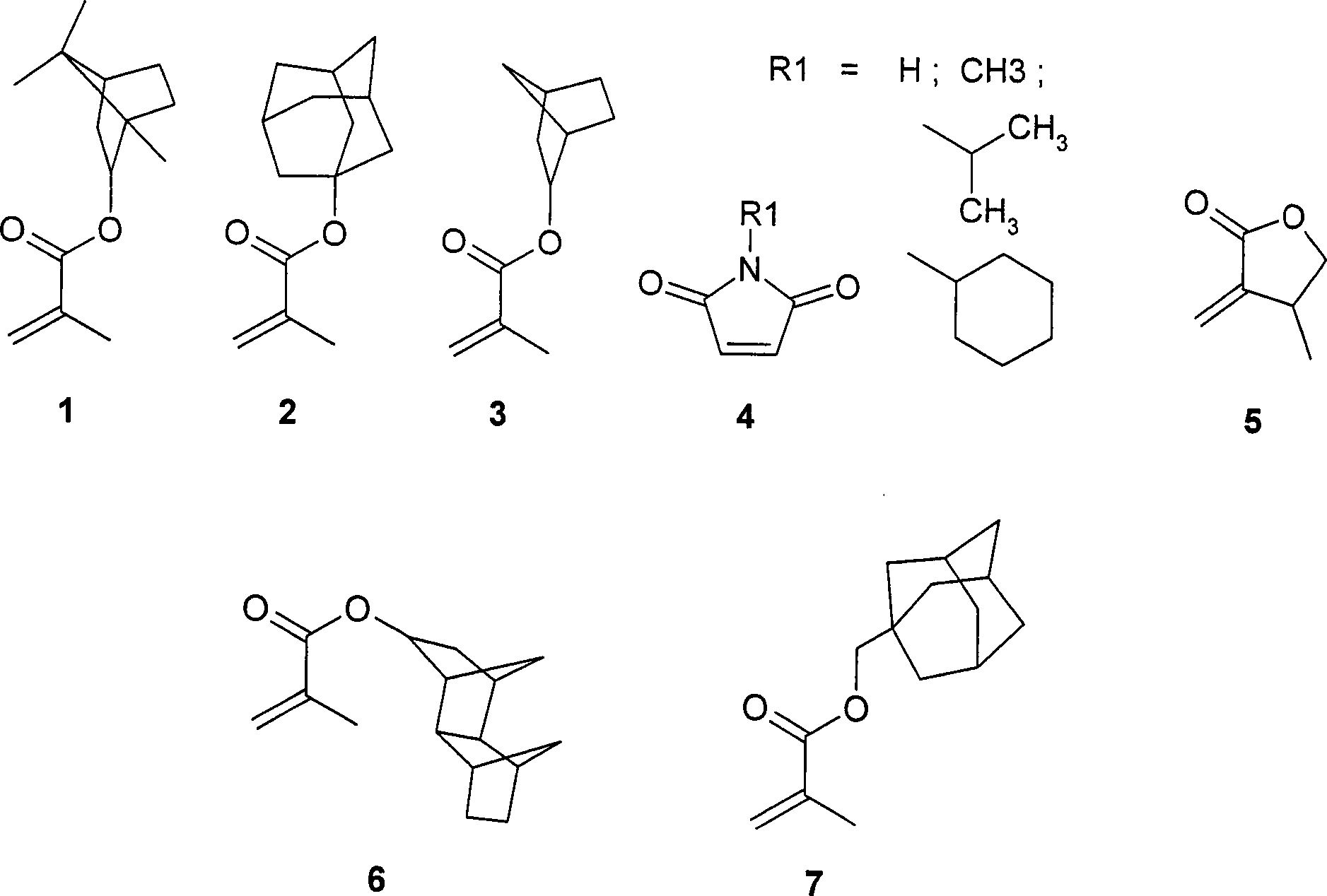
- (b) Monomeren mit vernetzbaren Seitengruppen und wahlweise mit (c) Methylmethacrylat zur Optimierung der mechanischen Eigenschaften, wobei weitere Monomere der Klasse (a) (1) 1-3 und 6-7 mit Fluor in der Estergruppe (2) 1 und 7 mit Dimethylsubstitution am Polyzyklus, gegebenenfalls fluoriert, und (3)
 sind, und weitere Monomere der Klasse (b) (1) 8 mit Methyl- oder Dimethyl-Substitution am Trizyklus, gegebenenfalls fluoriert, (2) 9 mit Methyl- oder mehrfacher Methyl-Substitution am Ester-Substituent sind.
- (A)
- (b) Monomers with crosslinkable side groups and optionally with (c) methyl methacrylate to optimize the mechanical properties, further monomers of classes (a) (1) 1-3 and 6-7 with fluorine in the ester group (2) 1 and 7 with dimethyl substitution on the polycycle, optionally fluorinated, and (3)are, and further monomers of class (b) (1) 8 with methyl or dimethyl substitution on the tricyclic, optionally fluorinated, (2) 9 with methyl or multiple methyl substitution on the ester substituent.
Die erfindungsgemäße Zusammensetzung ist nicht spröde, umfasst lichtdurchlässige Polymere und weist eine Glasübergangstemperatur von über 145°C bis 300°C auf.The composition according to the invention is not brittle, includes translucent Polymers and has a glass transition temperature from above 145 ° C to 300 ° C.
Dabei werden Kombinationen von Monomeren eingesetzt, welche in einer geeigneten statistischen Aufeinanderfolge polymerisiert werden. Dazu kann z.B. die Software PREDICI zur Simulation der Polymerisation genutzt werden.Combinations of monomers used in a suitable statistical sequence be polymerized. For this, e.g. the PREDICI software for simulation the polymerization can be used.
Die Polymeren werden vorzugsweise durch radikalische Polymerisation hergestellt. Vorzugsweise wird dabei Azobisisobutyronitril als Radikalinitiator in aprotischen organischen Lösungsmittel bei 70 ± 15°C genutzt. Die statistische Reihenfolge der wiederkehrenden Einheiten in der Polymerkette kann mittels PREDICI ermittelt werden. Die oben gezeigten Monomeren 1 bis 7 dienen der Versteifung der Polymerkette und ergeben Polymere mit einer hohen Glasübergangstemperatur. Glasübergangstemperaturen von Methacrylathomopolymeren sind bei Cypcar (a.a.O., S. 8954) referiert. Sie können mit Methyl methacrylat kombiniert werden, um die mechanischen Eigenschaften zu optimieren, sofern dies erforderlich ist.The polymers are preferred produced by radical polymerization. Preferably Azobisisobutyronitrile as a radical initiator in aprotic organic solvents used at 70 ± 15 ° C. The statistical order of the recurring units in the Polymer chain can be determined using PREDICI. The ones shown above Monomers 1 to 7 serve to stiffen the polymer chain and result in polymers with a high glass transition temperature. Glass transition temperatures of methacrylate homopolymers are cited in Cypcar (op. cit., p. 8954). You can can be combined with methyl methacrylate to improve the mechanical properties to optimize if necessary.
Eine hohe Glasübergangstemperatur weisen Adamantyl-
und Isobornylester-methacrylat-Homopolymere auf. Bei Verwendung
der Verbindung 2 beispielsweise wird eine Glasübergangstemperatur von 183°C (Cypcar,
Camelio, Zazzeri, Mathias, Waegell, Macromolecules (1996), S. 8956
und zit. Lit.) und bei Verwendung von 1 ein Tg von 203°C (Allen,
Wallraff, Dipietro, Hofer, J. of Photopolymer Science and Technol.
7, (1974), S. 511, 515) beobachtet. Auch das Homopolymere 3-tetracyclododecylmethacrylat
weist einen hohen Tg auf: 204°C.
N-Alkylmaleimide 4 (
Die in der Polymer-Zusammensetzung
verwendeten Seitengruppen nach Klasse (b) dienen zusätzlich dazu,
die Glasübergangstemperatur
durch Vernetzen zu erhöhen.
Thermisch stabile aber verknüpfungsfähige Seitengruppen
sind für
die Wellenleiterkernverdichtung vorteilhaft: Dicyclopentenyl-methacrylat
8 und Furfuryl-methacrylat 9 enthaltende Polymere können besser
vernetzen:


Weitere Verbindungen sind nachfolgend
dargestellt:

Als alternative oder zusätzliche Komponenten können zum Beispiel durch Licht zersetzbare Farbstoffe (Spiro-Verbindungen) oder photothermisch differenziell abbaubare Chromophore (z.B. 5-Naphthochinondiazide) enthalten sein.As an alternative or additional Components can for example dyes that can be decomposed by light (spiro compounds) or photothermally differentially degradable chromophores (e.g. 5-naphthoquinonediazides) be included.
Die durch UV-Bestrahlung induzierten chemischen Reaktionen an der Polymerkette umfassen erfindungsgemäß:
- (i) Photodissoziation der α-Substituenten
- (ii) Seitenketten-Photolyse
- (iii) Vernetzung
- (iv) Radikalbildung an der Seitenkette
- (v) Rekombination
- (i) Photodissociation of the α-substituents
- (ii) Side chain photolysis
- (iii) networking
- (iv) radical formation on the side chain
- (v) recombination
Die zur Erzielung dieser Reaktionen erforderlichen Strahlungsquellen geben je nach Systemwahl Strahlung im nahen bis Vakuum-UV ab. Marktübliche Strahlungsquellen kommen dabei zur Anwendung. Je nach System bedarf es einer Optimierung der Strahlungsintensität. Beispielsweise erfordert eine 3 μm Schicht Polymethylmethacrylat auf einem Siliziumträger etwa 8 min Bestrahlung mit einer Xe-Hg-Bogenlampe bei 1 kW. Ähnliche Bedingungen gelten für alle aromatenfreie Polymethacrylate. Chrom- oder Aluminium-Photomasken können dabei verwendet werden.To achieve these reactions required radiation sources give radiation depending on the system choice in the near to vacuum UV. Customary Radiation sources are used. Depending on the system needs it an optimization of the radiation intensity. For example, requires a 3 μm Layer of polymethyl methacrylate on a silicon substrate, for example 8 min irradiation with an Xe-Hg arc lamp at 1 kW. Similar Conditions apply to all aromatic-free polymethacrylates. Chrome or aluminum photomasks can be used.
In einer bevorzugten Ausführungsform wird UV-Strahlung mit Wellenlängen 250 < λ < 280 nm und einer Strahlungsintensität von 1-2 mW/cm2 während 2-4 Stunden verwendet. Das Polymermaterial enthält dabei keinerlei Zusätze. Zum gleichen Zweck kann auch ein ArF-Laser bei 193 nm verwendet werden, jedoch muss eine geringe Strahlungsintensität verwendet werden, um Abtragung zu vermeiden.In a preferred embodiment, UV radiation with wavelengths 250 <λ <280 nm and a radiation intensity of 1-2 mW / cm 2 is used for 2-4 hours. The polymer material does not contain any additives. An ArF laser at 193 nm can also be used for the same purpose, but a low radiation intensity must be used to avoid ablation.
Die Arbeitsweise mit kurzwelligem UV, z.B. bei 254 nm führt zu allen Reaktionen (i) bis (v). Im Falle von reinem PMMA werden dabei kleinere Bruchstücke abgespalten (Miraoka, IBM J. Res. Dev. 21, 121 (1977)). Es kommt zu einem Volumenverlust und gleichzeitig zu einer Erhöhung des Brechungsindex in der bestrahlten Struktur. Dieser Volumenverlust ist bei PMMA gravierend (Frank, Passive components in plastic materials using surface modification by ionizing radiation, Proc. POF 98, Berlin, 273 (1998)).Working with short-wave UV, e.g. at 254 nm to all reactions (i) to (v). In the case of pure PMMA smaller fragments split off (Miraoka, IBM J. Res. Dev. 21, 121 (1977)). It is coming to a loss of volume and at the same time an increase in Refractive index in the irradiated structure. This loss of volume is serious at PMMA (Frank, Passive components in plastic materials using surface modification by ionizing radiation, Proc. POF 98, Berlin, 273 (1998)).
In der erfindungsgemäßen Ausführungsform werden Estergruppierungen in 1-11 und 15-18 verwendet, die weniger flüchtige Abspaltprodukte ergeben. Infolgedessen ist der Volumenverlust geringer und der Vernetzungsgrad höher. Letztere Eigenschaft führt eher zur Tg-Erhöhung im Gegensatz zur Tg-Erniedrigung beim PMMA. Es kommt erfindungsgemäß darauf an, bei Raumtemperatur die Prozesse (i) bis (v) gegenüber der Kettenspaltung bei gerade noch ausreichender Energie bevorzugt zum Zuge kommen zu lassen. Dabei können auch kurze aufeinanderfolgende Belichtungen vorteilhaft benutzt werden. Eine Temperung des Materials nach der Belichtung unterhalb der Tg-Temperatur führt zu verbesserter thermischer Stabilität.In the embodiment according to the invention ester groups are used in 1-11 and 15-18, the less volatile Splitting products result. As a result, the volume loss is less and the degree of crosslinking is higher. The latter property leads rather to increase Tg in contrast to the lowering of Tg in PMMA. It comes down to it according to the invention processes (i) to (v) compared to the Chain splitting with just enough energy preferred to To let trains come. You can even short successive exposures advantageously used become. A tempering of the material after exposure below the Tg temperature leads for improved thermal stability.
In einer weiteren Ausführungsform wird die photoinduzierte Seitenkettenspaltung oberhalb einer Bestrahlungswellenlänge von 260 nm zur Vernetzung der bestrahlten Strukturen genutzt, z.B. bei Verwendung von 15-18.In another embodiment the photoinduced side chain cleavage above an irradiation wavelength of 260 nm used to crosslink the irradiated structures, e.g. at Use 15-18.
In einer weiteren Ausführungsform wird die photoinduzierte Radikalbildung zur Vernetzung der bestrahlten Strukturen genutzt, z.B. bei Verwendung von 8 und 9. Letzteres vernetzt am Ring (Gandini, The Behaviour of Furan Derivatives in Polymerization Reactions, S. 57, 78).In another embodiment is the photo-induced radical formation to cross-link the irradiated Structures used, e.g. when using 8 and 9. The latter networked am Ring (Gandini, The Behavior of Furan Derivatives in Polymerization Reactions, pp. 57, 78).
In einer weiteren Ausführungsform wird die photoinduzierte Einpolymerisation von gelöstem Restmonomer zur Verdichtung der bestrahlten Strukturen genutzt, z.B. bei Verwendung von 1-9.In another embodiment is the photo-induced polymerization of dissolved residual monomer used to densify the irradiated structures, e.g. Using from 1-9.
Die Zersetzung von Polymethylmethacrylat (PMMA) durch Elektronenstrahlen (Frank, Passive components in plastic materials using surface modification by ionizing radiation, Proc. POF 98, Berlin, 273 (1998)) ist bekannt und untersucht: die Aufspaltung in Monomere hängt von der Strahlungsintensität ab und es kommt zu einer Rekombination. Beobachtet wurde ebenfalls die Härtung von Polymeren mittels Elektronenstrahl. Bekannt ist auch die Reaktivität von Polymethacrylaten gegenüber UV-Licht. UV-Licht kann auch mittels Laser erzeugt werden. Berichtet worden ist ebenfalls die Unlöslichkeit von Polymethacrylat bei UV-Belichtung (Tomlinson, Hamikow, Chandross, Fork, Silfrast Appl. Phy. Lett. S. 486 (1970)). Erfindungsgemäß kann im nahen UV zusätzlich ein thermisch beständiger Photoinitiator als Sensibilisator in der Seitenkette verwendet. Es dient gleichermaßen als Photovernetzer.The decomposition of polymethyl methacrylate (PMMA) by electron beams (Frank, Passive components in plastic materials using surface modification by ionizing radiation, Proc. POF 98, Berlin, 273 (1998)) is known and examined: the split depends in monomers on the radiation intensity off and there is a recombination. It was also observed the hardening of polymers using an electron beam. The reactivity of polymethacrylates is also known across from UV light. UV light can also be generated using a laser. reported insolubility has also become of polymethacrylate with UV exposure (Tomlinson, Hamikow, Chandross, Fork, Silfrast Appl. Phy. Lett. P. 486 (1970)). According to the invention near UV additionally a thermally stable Photoinitiator used as a sensitizer in the side chain. It serves equally as a photocrosslinker.
Ein Reaktionsbeispiel mit Dicyclopentenylmethacrylat
zur Herstellung vernetzter Muster ist nachfolgend formelmäßig dargestellt: 
Neben den wie vorstehend beschrieben herstellbaren Polymethacrylat-Zusammensetzungen können auch handelsübliche Polymethacrylat-Zusammensetzungen verwendet werden, sofern diese eine Glasübergangstemperatur über 145°C aufweisen. Solche Polymethaycrylat-Zusammensetzungen sind beispielsweise in „Wärmformbeständig und optisch brillant", Arnoldi, Dorn, Schwind, Haßkerl, Hauch in Kunststoffe 87 (1997), S. 734 beschrieben.In addition to those as described above producible polymethacrylate compositions can also commercial Polymethacrylate compositions are used, provided that these have a glass transition temperature above 145 ° C. Such polymethyl acrylate compositions are, for example, in “heat resistance and optically brilliant ", Arnoldi, Dorn, Schwind, Haßkerl, Hauch in Kunststoffe 87 (1997), p. 734.
Dabei hat ein Copolymer aus 40% 4-Methyl-3-methylendihydrofuran-2-on 5 mit MMA ein Tg von 182°C. Ein Terpolymer aus 5 mit MMA aber mit geringerem Anteil an MMA und dafür enthaltend 1, 2, 3, 4, 6, oder 7 führt zum mindestens gleichen oder höheren Tg, indem die innere Weichmachung (vgl. Hans-Georg Elias, Makromoleküle, S. 856 (1990)) des MMA herabgesetzt wird. MMA hat einen Tg von 105°C, während die Homopolymere der Ersatzkomponenten 1, 2, 3, 4, 6, oder 7 darüber liegen.A copolymer of 40% has 4-methyl-3-methylenedihydrofuran-2-one 5 with MMA a Tg of 182 ° C. A terpolymer of 5 with MMA but with a lower proportion of MMA and containing for it 1, 2, 3, 4, 6, or 7 leads at least the same or higher Tg, by the inner softening (cf.Hans-Georg Elias, Macromolecules, p. 856 (1990)) of the MMA is reduced. MMA has a Tg of 105 ° C, while the homopolymers the replacement components 1, 2, 3, 4, 6, or 7 are above.
Die Tg-Werte von Methacrylat-Polymeren lassen sich zuverlässig voraussagen wie von Cypcar et al. in Macromolecules, S. 8954ff. gezeigt. Die Theorie der Glasübergangstemperatur wird in Elias, S. 854ff. erläutert.The Tg values of methacrylate polymers can be reliable predict as suggested by Cypcar et al. in Macromolecules, pp. 8954ff. shown. The theory of glass transition temperature is in Elias, p. 854ff. explained.
Ein weiteres Ausführungsbeispiel sind Copolymere mit 1. Indem 42-5% MMA zum Isobornylmethacrylat 1 bei der Polymerisation zugefügt wird, entsteht ein Copolymer mit einer Tg-Temperatur von 170°C (Allen, Wallraff (a.a.O., S. 515)) und damit 33°C unterhalb der Tg-Temperatur des Homopolymers. Mehrkomponentige Copolymere mit 2 bis 10 oder 11 dienen nicht allein der Erzielung eines hohen Tg, sondern erlauben durch Zumischung dieser Monomere auch eine Optimierung der mechanischen Eigenschaften mittels synergistischer Effekte.Another embodiment is copolymers with 1. By 42-5% MMA to isobornyl methacrylate 1 in the polymerization added a copolymer with a Tg temperature of 170 ° C (Allen, Wallraff (op. Cit., P. 515)) and thus 33 ° C below the Tg temperature of the homopolymer. Multi-component copolymers with 2 to 10 or 11 not only serve to achieve a high Tg, but allow through Mixing these monomers also optimizes the mechanical Properties by means of synergistic effects.
In der vorliegenden Erfindung werden verbesserte Zusammensetzungen von Hoch-Tg-Polymethacrylaten erhalten, indem Co-, Ter-, Tetra- und Penta-Polymerisationen statistisch modelliert werden.In the present invention obtain improved compositions of high Tg polymethacrylates, by statistically modeling Co, Ter, Tetra and Penta polymerizations become.
Die Modellierung ermöglicht höhere Molekulargewichte als bei der ungesteuerten Lösungspolymerisation. Darüber hinaus kann mit Modellierungs-Software eine statistisch homogene Verteilung der Monomere in der Polymerkette eingestellt werden (vgl. Deuflhard, Wulkow, Simulationsverfahren für die Polymerchemie, Preprint SC 94-22 (August 1994), Konrad-Zuse-Zentrum für Informationstechnik Berlin). Eine der vielen Möglichkeiten zur Gewinnung der Optimierungsparameter beschreiben Maeder und Renken in DECHEMA Monographs 131 (1995), S. 433. Die Anforderung nach molekularer Homogenität in Wellenleitern für geringe Dispersionsverluste ist allgemein bekannt. Erfindungsgemäß wird diese Aufgabenstellung durch Modellierung der Polymerisation wie beschrieben gelöst. Ohne Modellierung bilden sich in der Polymerkette bevorzugte Monomer-Regionen gemäß ihrer Reaktivität (vgl. Deuflhard, S. 15), ein Nachteil für die mechanischen und optischen Eigenschaften.The modeling enables higher molecular weights than in uncontrolled solution polymerization. About that In addition, modeling software can provide a statistically homogeneous distribution of the monomers in the polymer chain can be adjusted (see Deuflhard, Wulkow, simulation method for Polymer Chemistry, Preprint SC 94-22 (August 1994), Konrad Zuse Center for Information Technology Berlin). One of the many options Maeder and Renken describe how to obtain the optimization parameters in DECHEMA Monographs 131 (1995), p. 433. The requirement for molecular homogeneity in waveguides for low dispersion losses are generally known. According to the invention Task by modeling the polymerization as described solved. Without modeling, preferred monomer regions form in the polymer chain according to their Reactivity (see Deuflhard, p. 15), a disadvantage for the mechanical and optical properties.
Ein Nachteil von Hoch-Tg-Zusammensetzungen ist, dass nach dem Auftragen und Trocknen der Polymerlösung sich innere Spannungen ergeben können. Dieses wird durch Tempern unterhalb des Tg's vermieden. Dabei können konventionelle Öfen, Infrarot- und Mikrowellenstrahlung eingesetzt werden.A disadvantage of high Tg compositions is that after applying and drying the polymer solution can result in internal tensions. This is avoided by tempering below the Tg. Conventional ovens, infrared and microwave radiation are used.
Synthesevorschriften für die Polymerisation der Methacrylsäureester in Lösung sind in Makromolekulare Stoffe, Methoden der Org. Chemie, Houben-Weyl Müller, Band XIV 1, S. 1044-1048, Makromolekulare Stoffe, Band E20 Teil 2, S. 1144-1149, 1156-1160 beschrieben.Synthesis instructions for the polymerization of methacrylic acid esters in solution are in macromolecules lare substances, methods of Org. Chemie, Houben-Weyl Müller, volume XIV 1, pp. 1044-1048, macromolecular substances, volume E20 part 2, pp. 1144-1149, 1156-1160.
Auch die Photopolymerisation kann zur Herstellung der Copolymere genutzt werden. Davidenko, Peniche, Sastre, San Roman in J. of Polym. Science, Part A, Polymer Chemistry 54 (1996), S. 1753).Photopolymerization can also can be used to produce the copolymers. Davidenko, Peniche, Sastre, San Roman in J. of Polym. Science, Part A, Polymer Chemistry 54 (1996), p. 1753).
Zur Bestimmung der Glasübergangstemperatur werden handelsübliche Methoden eingesetzt, eine Zusammenstellung findet sich bei Behrstein, Egorov in „Differential Scanning Calorimetry of Polymers", S. 134 (1994).To determine the glass transition temperature become commercially available Methods used, a compilation can be found at Behrstein, Egorov in “Differential Scanning Calorimetry of Polymers ", P. 134 (1994).
Die angeführten Monomere sind vielfach käuflich erhältlich, z.B. 1-Adamantylmethacrylat von Fa. BIMAX, Isobornylmethacrylat von Fa. Atofina, Norbornylmethacrylat von Fa. Aldrich, Dicyclopentenylmethacrylat von Fa. Hitachi Chemical, Furfurylmethacrylat von Fa. Aldrich und ebenso Sensibilisatoren, wie z.B. der 2-Methylacrylsäure-5,8-dioxo-5,8-dihydronaphthalen-1-yl-Ester.The listed monomers are many for sale available, e.g. 1-Adamantyl methacrylate from BIMAX, isobornyl methacrylate from Atofina, norbornyl methacrylate from Aldrich, dicyclopentenyl methacrylate from Hitachi Chemical, furfuryl methacrylate from Aldrich and the like Sensitizers such as the 2-methylacrylic acid-5,8-dioxo-5,8-dihydronaphthalene-1-yl ester.
Claims (28)


Priority Applications (1)
| Application Number | Priority Date | Filing Date | Title |
|---|---|---|---|
| DE2002152563 DE10252563A1 (en) | 2002-06-27 | 2002-11-12 | A process for preparation of planar, optical waveguides useful for optical, electrooptical, or hybrid systems or for the preparation of electrooptical structural elements or hybrid electrooptical guide plates |
Applications Claiming Priority (3)
| Application Number | Priority Date | Filing Date | Title |
|---|---|---|---|
| DE10228745.7 | 2002-06-27 | ||
| DE10228745 | 2002-06-27 | ||
| DE2002152563 DE10252563A1 (en) | 2002-06-27 | 2002-11-12 | A process for preparation of planar, optical waveguides useful for optical, electrooptical, or hybrid systems or for the preparation of electrooptical structural elements or hybrid electrooptical guide plates |
Publications (1)
| Publication Number | Publication Date |
|---|---|
| DE10252563A1 true DE10252563A1 (en) | 2004-01-29 |
Family
ID=29795904
Family Applications (1)
| Application Number | Title | Priority Date | Filing Date |
|---|---|---|---|
| DE2002152563 Ceased DE10252563A1 (en) | 2002-06-27 | 2002-11-12 | A process for preparation of planar, optical waveguides useful for optical, electrooptical, or hybrid systems or for the preparation of electrooptical structural elements or hybrid electrooptical guide plates |
Country Status (3)
| Country | Link |
|---|---|
| AU (1) | AU2003246626A1 (en) |
| DE (1) | DE10252563A1 (en) |
| WO (1) | WO2004003609A1 (en) |
Citations (1)
| Publication number | Priority date | Publication date | Assignee | Title |
|---|---|---|---|---|
| CA2387716A1 (en) * | 2000-08-29 | 2002-03-07 | Jsr Corporation | Radiation sensitive refractive index changing composition and refractive index changing method |
Family Cites Families (8)
| Publication number | Priority date | Publication date | Assignee | Title |
|---|---|---|---|---|
| JPH01134309A (en) * | 1987-11-19 | 1989-05-26 | Fujitsu Ltd | Production of light guide |
| US5292620A (en) * | 1988-01-15 | 1994-03-08 | E. I. Du Pont De Nemours And Company | Optical waveguide devices, elements for making the devices and methods of making the devices and elements |
| EP0412675B1 (en) * | 1989-08-08 | 1995-06-07 | Imperial Chemical Industries Plc | Optical components |
| US5136682A (en) * | 1991-04-15 | 1992-08-04 | Raychem Corporation | Curable compositions and methods for use in forming optical waveguide structures |
| JP3130165B2 (en) * | 1993-03-01 | 2001-01-31 | 三菱レイヨン株式会社 | Transparent resin composition |
| US6306563B1 (en) * | 1999-06-21 | 2001-10-23 | Corning Inc. | Optical devices made from radiation curable fluorinated compositions |
| JP2003515782A (en) * | 1999-12-02 | 2003-05-07 | ジェムファイア コーポレイション | Optical definition of optical devices |
| ATE433129T1 (en) * | 2000-06-15 | 2009-06-15 | 3M Innovative Properties Co | MICROMANUFACTURING PROCESS FOR ORGANIC OPTICAL COMPONENTS |
-
2002
- 2002-11-12 DE DE2002152563 patent/DE10252563A1/en not_active Ceased
-
2003
- 2003-06-27 AU AU2003246626A patent/AU2003246626A1/en not_active Abandoned
- 2003-06-27 WO PCT/EP2003/006859 patent/WO2004003609A1/en not_active Application Discontinuation
Patent Citations (1)
| Publication number | Priority date | Publication date | Assignee | Title |
|---|---|---|---|---|
| CA2387716A1 (en) * | 2000-08-29 | 2002-03-07 | Jsr Corporation | Radiation sensitive refractive index changing composition and refractive index changing method |
Non-Patent Citations (3)
| Title |
|---|
| ALLEN, R.D. et al.: Single Layer Resists with En- hanced Etch Resistance for 193 nm Lithography. In: J. of Photopolymer Science and Technology, Vol.7, No. 3 (1994) S. 507-516 |
| ALLEN, R.D. et al.: Single Layer Resists with En- hanced Etch Resistance for 193 nm Lithography. In: J. of Photopolymer Science and Technology, Vol.7,No. 3 (1994) S. 507-516 * |
| CYPCAR,C.C. et al.: Prediction on the Glass Tran- sition Temperature of Multicycle and Bulky Sub- stituted Acrylate and Methacrylate Polymers Using the Energy, Volume, Mass (EVM) QSPR Model. In: Macromolecures 1996, 29, S. 8954-8959 * |
Also Published As
| Publication number | Publication date |
|---|---|
| AU2003246626A1 (en) | 2004-01-19 |
| WO2004003609A1 (en) | 2004-01-08 |
Similar Documents
| Publication | Publication Date | Title |
|---|---|---|
| DE60114820T2 (en) | MICRO MANUFACTURING PROCESS FOR ORGANIC OPTICAL COMPONENTS | |
| DE69433402T2 (en) | POLYMERIC MICROSTRUCTURES THAT SIMPLIFY THE COUPLING BETWEEN AN OPTICAL FIBER AND A WAVE GUIDE | |
| DE69816605T2 (en) | METHOD FOR PRODUCING AN OPTICAL ELEMENT AND OPTICAL ELEMENT THEREOF | |
| DE69030234T2 (en) | LIGHT CROSSLINKABLE PLASTIC LAMINATE AND METHOD FOR PRODUCING A PRINTED CIRCUIT BOARD UNDER THE USE THEREOF | |
| DE60005848T2 (en) | ELEMENT AND METHOD FOR SPLICING OPTICAL FIBERS | |
| DE69735946T2 (en) | OPTICAL LADDER | |
| EP0186091B1 (en) | Dry resist film and process for producing resist patterns | |
| EP0442071B1 (en) | Process for the production of photostructured layers with improved mechanical properties | |
| JP2004503813A (en) | Multiphoton curing to provide encapsulated optics | |
| DE2004214A1 (en) | A method of reproducing images using a photohardenable material | |
| DE2249518A1 (en) | METHOD FOR MANUFACTURING OPTICAL WAVE CONDUCTOR COMPONENTS | |
| DE60023562T2 (en) | LIGHT-RESISTANT MICROLINE ARRAY AND RESIN COMPOSITION FOR USE THEREIN | |
| EP0141389A2 (en) | Process for the production of image-wise structured resists, and dry resist therefor | |
| DE69019889T2 (en) | Optical component. | |
| DE3824903A1 (en) | PHOTOPOLYMERIZABLE MIXTURE AND RECORDING MATERIAL MADE THEREOF | |
| DE19641655B4 (en) | Method for producing an optical device | |
| DE69126271T2 (en) | Negative working, photosensitive electrodeposition resin composition | |
| DE69209827T2 (en) | Polymeric nitrones with an acrylic main chain | |
| DE69122159T2 (en) | Slit coupling of optical waveguide into optical waveguide components | |
| DE3732801C2 (en) | ||
| EP0048899B1 (en) | Method of producing resist patterns | |
| KR100705759B1 (en) | Manufacturing Method for Planar Multimode Optical Waveguide by Direct Photopatterning | |
| DE68927446T2 (en) | Optical waveguides, elements for the manufacture of these devices and manufacturing processes for these elements and devices | |
| DE10252563A1 (en) | A process for preparation of planar, optical waveguides useful for optical, electrooptical, or hybrid systems or for the preparation of electrooptical structural elements or hybrid electrooptical guide plates | |
| DE3447356A1 (en) | LIGHT SENSITIVE RECORDING ELEMENT |
Legal Events
| Date | Code | Title | Description |
|---|---|---|---|
| OP8 | Request for examination as to paragraph 44 patent law | ||
| 8131 | Rejection |