DE102018009813A1 - Compensation of an input current of an LDO power amplifier - Google Patents
Compensation of an input current of an LDO power amplifier Download PDFInfo
- Publication number
- DE102018009813A1 DE102018009813A1 DE102018009813.4A DE102018009813A DE102018009813A1 DE 102018009813 A1 DE102018009813 A1 DE 102018009813A1 DE 102018009813 A DE102018009813 A DE 102018009813A DE 102018009813 A1 DE102018009813 A1 DE 102018009813A1
- Authority
- DE
- Germany
- Prior art keywords
- transistor
- resistor
- input
- current
- compensation circuit
- Prior art date
- Legal status (The legal status is an assumption and is not a legal conclusion. Google has not performed a legal analysis and makes no representation as to the accuracy of the status listed.)
- Pending
Links
- 239000000872 buffer Substances 0.000 claims abstract description 63
- 238000000034 method Methods 0.000 claims description 9
- 239000003990 capacitor Substances 0.000 claims description 7
- 238000001914 filtration Methods 0.000 claims description 4
- 238000010586 diagram Methods 0.000 description 4
- 230000002411 adverse Effects 0.000 description 3
- 238000013459 approach Methods 0.000 description 3
- 239000004065 semiconductor Substances 0.000 description 3
- 238000000342 Monte Carlo simulation Methods 0.000 description 2
- 238000004519 manufacturing process Methods 0.000 description 2
- 238000012986 modification Methods 0.000 description 2
- 230000004048 modification Effects 0.000 description 2
- 238000001228 spectrum Methods 0.000 description 2
- JBRZTFJDHDCESZ-UHFFFAOYSA-N AsGa Chemical compound [As]#[Ga] JBRZTFJDHDCESZ-UHFFFAOYSA-N 0.000 description 1
- JMASRVWKEDWRBT-UHFFFAOYSA-N Gallium nitride Chemical compound [Ga]#N JMASRVWKEDWRBT-UHFFFAOYSA-N 0.000 description 1
- 206010073261 Ovarian theca cell tumour Diseases 0.000 description 1
- XUIMIQQOPSSXEZ-UHFFFAOYSA-N Silicon Chemical compound [Si] XUIMIQQOPSSXEZ-UHFFFAOYSA-N 0.000 description 1
- 230000006978 adaptation Effects 0.000 description 1
- -1 but not limited to Substances 0.000 description 1
- 230000000593 degrading effect Effects 0.000 description 1
- 230000005611 electricity Effects 0.000 description 1
- 230000001771 impaired effect Effects 0.000 description 1
- 238000004806 packaging method and process Methods 0.000 description 1
- 230000000630 rising effect Effects 0.000 description 1
- 229910052710 silicon Inorganic materials 0.000 description 1
- 239000010703 silicon Substances 0.000 description 1
- HBMJWWWQQXIZIP-UHFFFAOYSA-N silicon carbide Chemical compound [Si+]#[C-] HBMJWWWQQXIZIP-UHFFFAOYSA-N 0.000 description 1
- 238000006467 substitution reaction Methods 0.000 description 1
- 239000000758 substrate Substances 0.000 description 1
Images


Classifications
-
- G—PHYSICS
- G05—CONTROLLING; REGULATING
- G05F—SYSTEMS FOR REGULATING ELECTRIC OR MAGNETIC VARIABLES
- G05F1/00—Automatic systems in which deviations of an electric quantity from one or more predetermined values are detected at the output of the system and fed back to a device within the system to restore the detected quantity to its predetermined value or values, i.e. retroactive systems
- G05F1/10—Regulating voltage or current
- G05F1/46—Regulating voltage or current wherein the variable actually regulated by the final control device is DC
- G05F1/56—Regulating voltage or current wherein the variable actually regulated by the final control device is DC using semiconductor devices in series with the load as final control devices
- G05F1/575—Regulating voltage or current wherein the variable actually regulated by the final control device is DC using semiconductor devices in series with the load as final control devices characterised by the feedback circuit
-
- G—PHYSICS
- G05—CONTROLLING; REGULATING
- G05F—SYSTEMS FOR REGULATING ELECTRIC OR MAGNETIC VARIABLES
- G05F1/00—Automatic systems in which deviations of an electric quantity from one or more predetermined values are detected at the output of the system and fed back to a device within the system to restore the detected quantity to its predetermined value or values, i.e. retroactive systems
- G05F1/10—Regulating voltage or current
- G05F1/46—Regulating voltage or current wherein the variable actually regulated by the final control device is DC
- G05F1/468—Regulating voltage or current wherein the variable actually regulated by the final control device is DC characterised by reference voltage circuitry, e.g. soft start, remote shutdown
-
- G—PHYSICS
- G05—CONTROLLING; REGULATING
- G05F—SYSTEMS FOR REGULATING ELECTRIC OR MAGNETIC VARIABLES
- G05F3/00—Non-retroactive systems for regulating electric variables by using an uncontrolled element, or an uncontrolled combination of elements, such element or such combination having self-regulating properties
- G05F3/02—Regulating voltage or current
- G05F3/08—Regulating voltage or current wherein the variable is DC
- G05F3/10—Regulating voltage or current wherein the variable is DC using uncontrolled devices with non-linear characteristics
- G05F3/16—Regulating voltage or current wherein the variable is DC using uncontrolled devices with non-linear characteristics being semiconductor devices
- G05F3/20—Regulating voltage or current wherein the variable is DC using uncontrolled devices with non-linear characteristics being semiconductor devices using diode- transistor combinations
- G05F3/24—Regulating voltage or current wherein the variable is DC using uncontrolled devices with non-linear characteristics being semiconductor devices using diode- transistor combinations wherein the transistors are of the field-effect type only
- G05F3/242—Regulating voltage or current wherein the variable is DC using uncontrolled devices with non-linear characteristics being semiconductor devices using diode- transistor combinations wherein the transistors are of the field-effect type only with compensation for device parameters, e.g. channel width modulation, threshold voltage, processing, or external variations, e.g. temperature, loading, supply voltage
- G05F3/247—Regulating voltage or current wherein the variable is DC using uncontrolled devices with non-linear characteristics being semiconductor devices using diode- transistor combinations wherein the transistors are of the field-effect type only with compensation for device parameters, e.g. channel width modulation, threshold voltage, processing, or external variations, e.g. temperature, loading, supply voltage producing a voltage or current as a predetermined function of the supply voltage
-
- G—PHYSICS
- G05—CONTROLLING; REGULATING
- G05F—SYSTEMS FOR REGULATING ELECTRIC OR MAGNETIC VARIABLES
- G05F3/00—Non-retroactive systems for regulating electric variables by using an uncontrolled element, or an uncontrolled combination of elements, such element or such combination having self-regulating properties
- G05F3/02—Regulating voltage or current
- G05F3/08—Regulating voltage or current wherein the variable is DC
- G05F3/10—Regulating voltage or current wherein the variable is DC using uncontrolled devices with non-linear characteristics
- G05F3/16—Regulating voltage or current wherein the variable is DC using uncontrolled devices with non-linear characteristics being semiconductor devices
- G05F3/20—Regulating voltage or current wherein the variable is DC using uncontrolled devices with non-linear characteristics being semiconductor devices using diode- transistor combinations
- G05F3/26—Current mirrors
- G05F3/265—Current mirrors using bipolar transistors only
Landscapes
- Engineering & Computer Science (AREA)
- Physics & Mathematics (AREA)
- Electromagnetism (AREA)
- General Physics & Mathematics (AREA)
- Radar, Positioning & Navigation (AREA)
- Automation & Control Theory (AREA)
- Microelectronics & Electronic Packaging (AREA)
- Nonlinear Science (AREA)
- Continuous-Control Power Sources That Use Transistors (AREA)
Abstract
Nach einem Aspekt, beinhaltet ein Low-Dropout (LDO) Regler einen Vorladungspuffer, eine Endstufe, und einen Rauschfilter, der zwischen den Vorladungspuffer und die Endstufe des LDO-Reglers geschaltet ist. Der Rauschfilter weist einen ersten Widerstand auf. Der LDO-Regler beinhaltet einen Transistor, der als Eingang zur Endstufe ausgebildet ist, und eine Kompensationsschaltung, die mit einem Eingang des Vorladungspuffers verbunden ist. Die Kompensationsschaltung weist einen zweiten Widerstand auf. Die Kompensationsschaltung ist dazu ausgebildet, einen Kompensationsstrom bereitzustellen, der einen ersten Spannungsabfall am zweiten Widerstand erzeugt, wobei der erste Spannungsabfall einen zweiten Spannungsabfall kompensiert, der am ersten Widerstand durch einen Eingangsstrom des Transistors erzeugt wird.In one aspect, a low dropout (LDO) regulator includes a precharge buffer, an output stage, and a noise filter connected between the precharge buffer and the output stage of the LDO regulator. The noise filter has a first resistance. The LDO regulator includes a transistor formed as an input to the final stage and a compensation circuit connected to an input of the precharge buffer. The compensation circuit has a second resistor. The compensation circuit is configured to provide a compensation current that produces a first voltage drop across the second resistor, the first voltage drop compensating for a second voltage drop generated at the first resistor by an input current of the transistor.
Description
Technisches GebietTechnical area
Die vorliegende Beschreibung bezieht sich auf die Kompensation eines Eingangsstroms einer Endstufe in einem Low-Dropout (LDO) Regler.The present description relates to the compensation of an input current of an output stage in a low-dropout (LDO) controller.
Hintergrundbackground
Ein LDO-Regler ist ein linearer Gleichstrom(DC)-Spannungsregler, der die Ausgangsspannung selbst dann regelt, wenn die Versorgungsspannung nahe der Ausgangsspannung liegt. Bei einigen LDO-Reglern kann die Ausgangsspannung durch Spannungsabfälle an im LDO-Regler enthaltenen Komponenten unerwünscht beeinflusst werden.An LDO regulator is a linear DC (DC) voltage regulator that regulates the output voltage even when the supply voltage is close to the output voltage. In some LDO controllers, the output voltage may be adversely affected by voltage drops across components contained in the LDO regulator.
ÜbersichtOverview
Nach einem Aspekt, beinhaltet ein Low-Dropout (LDO) Regler einen Vorladungspuffer, eine Endstufe, und einen Rauschfilter, der zwischen den Vorladungspuffer und die Endstufe des LDO-Reglers geschaltet ist. Der Rauschfilter weist einen ersten Widerstand auf. Der LDO-Regler beinhaltet einen Transistor, der als Eingang zu der Endstufe ausgebildet ist, und eine Kompensationsschaltung, die mit einem Eingang des Vorladungspuffers verbunden ist. Die Kompensationsschaltung weist einen zweiten Widerstand auf. Die Kompensationsschaltung ist dazu ausgebildet, einen Kompensationsstrom bereitzustellen, der einen ersten Spannungsabfall am zweiten Widerstand erzeugt, wobei der erste Spannungsabfall einen zweiten Spannungsabfall kompensiert, der am ersten Widerstand durch einen Eingangsstrom des Transistors erzeugt wird.In one aspect, a low dropout (LDO) regulator includes a precharge buffer, an output stage, and a noise filter connected between the precharge buffer and the output stage of the LDO regulator. The noise filter has a first resistance. The LDO regulator includes a transistor formed as an input to the final stage and a compensation circuit connected to an input of the precharge buffer. The compensation circuit has a second resistor. The compensation circuit is configured to provide a compensation current that produces a first voltage drop across the second resistor, the first voltage drop compensating for a second voltage drop generated at the first resistor by an input current of the transistor.
Nach einigen Aspekten kann der LDO-Regler eines oder mehrere der folgenden Merkmale (oder eine beliebige Kombination davon) beinhalten. Der Transistor ist ein Bipolartransistor (BJT). Der Kompensationsstrom entspricht dem Eingangsstrom des Transistors. Der zweite Widerstand hat einen Widerstandswert, der gleich einem Widerstandswert des ersten Widerstands ist. Der Eingang des Vorladungspuffers ist ein erster Eingang, und der Vorladungspuffer weist einen zweiten Eingang auf, der zum Aufnehmen einer Referenzspannung ausgebildet ist. Die Kompensationsschaltung weist einen Transistor auf, der mit dem zweiten Widerstand verbunden ist, wobei der Kompensationsstrom ein Eingangsstrom des Transistors der Kompensationsschaltung ist. Der Transistor der Kompensationsschaltung ist ein Bipolartransistor (BJT). Der erste Spannungsabfall entspricht dem zweiten Spannungsabfall. Die Endstufe weist einen Spannungsverstärker mit einem Eingang auf, und der Eingang des Spannungsverstärkers ist mit dem Transistor verbunden.In some aspects, the LDO regulator may include one or more of the following features (or any combination thereof). The transistor is a bipolar transistor (BJT). The compensation current corresponds to the input current of the transistor. The second resistor has a resistance equal to a resistance of the first resistor. The input of the precharge buffer is a first input, and the precharge buffer has a second input configured to receive a reference voltage. The compensation circuit has a transistor connected to the second resistor, the compensation current being an input current of the transistor of the compensation circuit. The transistor of the compensation circuit is a bipolar transistor (BJT). The first voltage drop corresponds to the second voltage drop. The output stage has a voltage amplifier with an input, and the input of the voltage amplifier is connected to the transistor.
Nach einem Aspekt beinhaltet ein LDO-Regler einen Referenzspannungsgenerator, der dazu ausgebildet ist, eine Referenzspannung zu erzeugen, und einen Vorladungspuffer mit einem ersten Eingang und einem zweiten Eingang, wobei der erste Eingang dazu ausgebildet ist, die Referenzspannung aufzunehmen. Der LDO-Regler beinhaltet eine Endstufe und einen Rauschfilter, der zwischen den Vorladungspuffer und die Endstufe des LDO-Reglers geschaltet ist. Der Rauschfilter beinhaltet einen ersten Widerstand und einen Kondensator. Der LDO-Regler beinhaltet einen Transistor, der als Eingang zu der Endstufe ausgebildet ist, und eine Kompensationsschaltung, die mit dem zweiten Eingang des Vorladungspuffers verbunden ist. Die Kompensationsschaltung beinhaltet einen zweiten Widerstand. Die Kompensationsschaltung ist dazu ausgebildet, einen Kompensationsstrom bereitzustellen, der einen ersten Spannungsabfall am zweiten Widerstand erzeugt, wobei der erste Spannungsabfall einen zweiten Spannungsabfall kompensiert, der am ersten Widerstand durch einen Eingangsstrom des Transistors erzeugt wird. Die Endstufe ist dazu ausgebildet, eine Ausgangsspannung zu erzeugen, die im Wesentlichen gleich der Referenzspannung ist.In one aspect, an LDO regulator includes a reference voltage generator configured to generate a reference voltage and a precharge buffer having a first input and a second input, the first input configured to receive the reference voltage. The LDO regulator includes an output stage and a noise filter connected between the precharge buffer and the LDO regulator power stage. The noise filter includes a first resistor and a capacitor. The LDO regulator includes a transistor formed as an input to the final stage and a compensation circuit connected to the second input of the precharge buffer. The compensation circuit includes a second resistor. The compensation circuit is configured to provide a compensation current that produces a first voltage drop across the second resistor, the first voltage drop compensating for a second voltage drop generated at the first resistor by an input current of the transistor. The output stage is designed to generate an output voltage that is substantially equal to the reference voltage.
Nach einigen Aspekten, kann der LDO-Regler eines oder mehrere der folgenden Merkmale (oder eine beliebige Kombination davon) beinhalten. Der Transistor ist ein Bipolartransistor (BJT). Der Kompensationsstrom entspricht dem Eingangsstrom des Transistors, und der zweite Widerstand hat einen Widerstandswert, der gleich einem Widerstandswert des ersten Widerstands ist. Die Kompensationsschaltung beinhaltet einen Transistor und einen Stromspiegel. Der Stromspiegel ist dazu ausgebildet, den Eingangsstrom des Transistors zu spiegeln und den gespiegelten Eingangsstrom als Eingangsstrom des Transistors der Kompensationsschaltung bereitzustellen, wobei der Eingangsstrom des Transistors der Kompensationsschaltung der Kompensationsstrom ist. Die Endstufe beinhaltet einen Spannungsverstärker und einen Transistor. Der LDO-Regler beinhaltet einen ersten Schalter, der mit dem ersten Widerstand verbunden ist, einen zweiten Schalter, der mit dem zweiten Widerstand verbunden ist, und einen Vorlade-Timer, der dazu ausgebildet ist, ein Öffnen und ein Schließen des ersten Schalters und des zweiten Schalters als Reaktion auf ein Freigabesignal zu steuern. Der erste Spannungsabfall entspricht dem zweiten Spannungsabfall. Der LDO-Regler beinhaltet einen Transistor, der mit einem Ausgang des Vorladungspuffers verbunden ist, wobei der Transistor mit einem Knoten verbunden ist, der zwischen dem ersten Widerstand und dem zweiten Widerstand angeordnet ist. Die Kompensationsschaltung beinhaltet einen mit dem zweiten Widerstand verbundenen Transistor, wobei der Kompensationsstrom ein Eingangsstrom des Transistors der Kompensationsschaltung ist.In some aspects, the LDO regulator may include one or more of the following features (or any combination thereof). The transistor is a bipolar transistor (BJT). The compensation current corresponds to the input current of the transistor, and the second resistor has a resistance value equal to a resistance value of the first resistor. The compensation circuit includes a transistor and a current mirror. The current mirror is configured to mirror the input current of the transistor and to provide the mirrored input current as the input current of the transistor of the compensation circuit, wherein the input current of the transistor of the compensation circuit is the compensation current. The power amplifier includes a voltage amplifier and a transistor. The LDO regulator includes a first switch connected to the first resistor, a second switch connected to the second resistor, and a precharge timer configured to open and close the first switch and the first switch second switch in response to a release signal to control. The first voltage drop corresponds to the second voltage drop. The LDO regulator includes a transistor connected to an output of the precharge buffer, the transistor being connected to a node disposed between the first resistor and the second resistor. The compensation circuit includes a transistor connected to the second resistor, wherein the compensation current is an input current of the transistor of the compensation circuit.
Nach einem Aspekt, beinhaltet ein Verfahren zum Verbessern der Leistung eines Low-Dropout (LDO) Reglers das Herausfiltern von Rauschen aus einer Referenzspannung unter Verwendung eines Rauschfilters, der zwischen einen Vorladungspuffer und eine Endstufe des LDO-Reglers geschaltet ist, wobei der Rauschfilter einen ersten Widerstand aufweist und ein Eingang des Vorladungspuffers mit einem Transistor verbunden ist, Bereitstellen eines Kompensationsstroms durch eine Kompensationsschaltung mit einem zweiten Widerstand, um einen ersten Spannungsabfall am zweiten Widerstand zu erzeugen, wobei der erste Spannungsabfall einen zweiten Spannungsabfall kompensiert, der am ersten Widerstand durch einen Eingangsstrom des Transistors erzeugt wird, und Erzeugen einer Ausgangsspannung in Abhängigkeit von der Referenzspannung. In one aspect, a method for improving the performance of a low-dropout (LDO) regulator includes filtering out noise from a reference voltage using a noise filter connected between a precharge buffer and an output stage of the LDO regulator, the noise filter having a first Resistor and an input of the precharge buffer is connected to a transistor, providing a compensation current through a compensation circuit with a second resistor to produce a first voltage drop across the second resistor, wherein the first voltage drop compensates for a second voltage drop, which at the first resistor by an input current of the transistor is generated, and generating an output voltage in dependence on the reference voltage.
Die Details einer oder mehrerer Implementierungen sind in den beigefügten Zeichnungen und der nachfolgenden Beschreibung enthalten. Weitere Merkmale ergeben sich aus der Beschreibung und den Zeichnungen sowie aus den Ansprüchen.The details of one or more implementations are included in the accompanying drawings and the description below. Further features will become apparent from the description and drawings and from the claims.
Figurenlistelist of figures
-
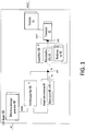
1 stellt einen LDO-Regler mit einer Kompensationsschaltung dar, die dazu ausgebildet ist, einen Eingangsstrom eines Transistors, der als Eingang zu einer Endstufe ausgebildet ist, nach einem Aspekt zu kompensieren.1 illustrates an LDO regulator with a compensation circuit, which is adapted to compensate an input current of a transistor, which is formed as an input to an output stage, in one aspect. -
2A stellt einen LDO-Regler mit einer Kompensationsschaltung nach einem anderen Aspekt dar.2A illustrates an LDO regulator with a compensation circuit according to another aspect. -
2B stellt den LDO-Regler der2A nach einem Aspekt dar.2 B sets the LDO regulator the2A according to one aspect. -
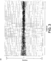
3 stellt ein Diagramm dar, das die Ergebnisse eines Temperaturverlaufs einer Monte-Carlo-Simulation nach einem Aspekt zeigt.3 FIG. 10 is a graph showing the results of a temperature history of a Monte Carlo simulation in one aspect. FIG. -
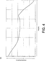
4 stellt ein Diagramm dar, das ein Rauschspektrum eines LDO-Reglers gemäß einem Aspekt zeigt.4 FIG. 12 is a diagram showing a noise spectrum of an LDO regulator according to one aspect. FIG. -
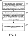
5 stellt ein Ablaufdiagramm dar, das exemplarische Operationen eines LDO-Reglers nach einem Aspekt zeigt.5 FIG. 10 is a flowchart showing exemplary operations of an LDO regulator according to one aspect. FIG.
Ausführliche BeschreibungDetailed description
Die vorliegende Offenbarung bezieht sich auf einen LDO-Regler mit einer Kompensationsschaltung, die dazu ausgebildet ist, beispielsweise einen durch den Eingangsstrom eines Bipolartransistors (BJT) einer Endstufe des LDO-Reglers verursachten Spannungsabfall eines Rauschfilters dadurch zu kompensieren, dass ein gleich großer Spannungsabfall am Eingang eines Vorladungspuffers des LDO-Reglers vorgesehen wird. Bei einigen Beispielen ist die Kompensationsschaltung, im Gegensatz zu manchen herkömmlichen Ansätzen, so ausgebildet, dass sie den Einfluss des Eingangsstroms des BJT-Eingangs der Endstufe kompensiert, selbst wenn der BJT-Eingang der Endstufe nur wenige mV unter der Versorgungsspannung liegt. Die Konfiguration der Kompensationsschaltung kann einen hochohmigen Widerstand im Rauschfilter zulassen, was das Rauschverhalten des LDO-Reglers verbessern kann.The present disclosure relates to an LDO regulator having a compensation circuit which is designed, for example, to compensate for a voltage drop of a noise filter caused by the input current of a bipolar transistor (BJT) of an output stage of the LDO regulator by causing an equal voltage drop at the input a precharge buffer of the LDO regulator is provided. In some examples, unlike some conventional approaches, the compensation circuit is designed to compensate for the influence of the input current of the BJT input of the output stage, even if the BJT input of the final stage is only a few mV below the supply voltage. The configuration of the compensation circuit can allow a high resistance in the noise filter, which can improve the noise performance of the LDO regulator.
Der LDO-Regler
Der Vorladungspuffer
Der Rauschfilter
Der Transistor
Der Eingangsstrom
Die Kompensationsschaltung
Die
Der LDO-Regler
Der LDO-Regler
Der LDO-Regler
Der Basisstrom
Der Referenzspannungsgenerator
Der Ausgang des Vorladungspuffers
Der Transistor
Wie hier besprochen, verursacht der Eingangsstrom
Beispielsweise können der Widerstand
So ist beispielsweise der Emitter des Transistors
Der LDO-Regler
Es wird darauf hingewiesen, dass die Spannung an der Drain des Transistors
Die Operation
Die Operation
Die Operation
Es versteht sich, dass in der vorstehenden Beschreibung, wenn ein Element als mit dem anderen Element verbunden, elektrisch verbunden, gekoppelt, oder elektrisch gekoppelt bezeichnet wird, es direkt mit dem anderen Element verbunden oder mit diesem gekoppelt sein kann, oder ein oder mehrere dazwischenliegende Elemente vorhanden sein können. Im Gegensatz dazu, wenn ein Element als direkt mit einem anderen Element verbunden oder direkt mit diesem gekoppelt bezeichnet wird, so sind keine dazwischenliegenden Elemente vorhanden. Obwohl die Begriffe direkt verbunden oder direkt gekoppelt möglicherweise nicht in der gesamten ausführlichen Beschreibung verwendet werden, können Elemente, die als direkt verbunden oder direkt gekoppelt dargestellt werden, als solche bezeichnet werden. Die Ansprüche der Anmeldung, falls vorhanden, können abgeändert werden, um exemplarische Beziehungen wiederzugeben, die in der Beschreibung beschrieben oder in den Figuren dargestellt sind. Implementierungen der verschiedenen hier beschriebenen Techniken können in digitalen elektronischen Schaltungen oder in Computerhardware, Firmware, Software oder in Kombinationen davon implementiert (z.B. darin einbezogen) werden. Teile von Verfahren können auch von einer speziellen Logikschaltung, z.B. einer FPGA [field programmable gate array (vor Ort programmierbaren (Logik-)Gatter-Anordnung)] oder einer ASIC [application specific integrated circuit (anwendungsspezifischen integrierten Schaltung)] durchgeführt werden, und eine Vorrichtung kann als solche implementiert werden.It should be understood that in the foregoing description, when one element is referred to as being connected to the other element, electrically connected, coupled, or electrically coupled, it may be directly connected to or coupled to the other element, or one or more intervening ones Elements can be present. In contrast, when an element is referred to as being directly connected to, or directly coupled to, another element, there are no intervening elements. Although the terms directly connected or directly coupled may not be used throughout the detailed description, elements that are shown as directly connected or directly coupled may be referred to as such. The claims of the application, if any, may be modified to reflect exemplary relationships described in the specification or illustrated in the figures. Implementations of the various techniques described herein may be implemented (e.g., incorporated) in digital electronic circuits or in computer hardware, firmware, software, or combinations thereof. Parts of methods may also be handled by a special logic circuit, e.g. an FPGA [Field Programmable Gate Array] or an ASIC [Application Specific Integrated Circuit], and a device may be implemented as such.
Einige Implementierungen können unter Verwendung verschiedener Halbleiterherstellungs- und/oder Packagingtechniken ausgeführt werden. Einige Implementierungen können unter Verwendung verschiedener Arten von Halbleiterherstellungstechniken ausgeführt werden, die mit Halbleitersubstraten, einschließlich, aber nicht beschränkt auf, beispielsweise Silizium (Si), Galliumarsenid (GaAs), Galliumnitrid (GaN), Siliziumkarbid (SiC) und/oder so weiter verbunden sind.Some implementations may be carried out using various semiconductor manufacturing and / or packaging techniques. Some implementations may be performed using various types of semiconductor fabrication techniques associated with semiconductor substrates, including, but not limited to, silicon (Si), gallium arsenide (GaAs), gallium nitride (GaN), silicon carbide (SiC), and / or so forth ,
Gemäß einem Aspekt umfasst ein Low-Dropout (LDO) Regler einen Vorladungspuffer, eine Endstufe und einen Rauschfilter, der zwischen den Vorladungspuffer und die Endstufe des LDO-Reglers geschaltet ist. Der Rauschfilter beinhaltet einen ersten Widerstand. Der LDO-Regler beinhaltet einen Transistor, der als Eingang zur Endstufe ausgebildet ist, und eine Kompensationsschaltung, die mit einem Eingang des Vorladungspuffers verbunden ist. Die Kompensationsschaltung beinhaltet einen zweiten Widerstand. Die Kompensationsschaltung ist dazu ausgebildet, einen Kompensationsstrom bereitzustellen, der einen ersten Spannungsabfall am zweiten Widerstand erzeugt, wobei der erste Spannungsabfall einen zweiten Spannungsabfall am ersten Widerstand kompensiert, der durch einen Eingangsstrom des Transistors erzeugt wird.In one aspect, a low dropout (LDO) regulator includes a precharge buffer, an output stage, and a noise filter connected between the precharge buffer and the output stage of the LDO regulator. The noise filter includes a first resistor. The LDO regulator includes a transistor formed as an input to the final stage and a compensation circuit connected to an input of the precharge buffer. The compensation circuit includes a second resistor. The compensation circuit is configured to provide a compensation current that produces a first voltage drop across the second resistor, the first voltage drop compensating for a second voltage drop across the first resistor generated by an input current of the transistor.
Nach einigen Aspekten ist der Kompensationsstrom gleich dem Eingangsstrom des Transistors, und der zweite Widerstand hat einen Widerstandswert, der gleich einem Widerstandswert des ersten Widerstands ist. Der Transistor ist ein Bipolartransistor (BJT), und der Eingang des Vorladungspuffers ist ein erster Eingang, und der Vorladungspuffer beinhaltet einen zweiten Eingang, der zum Aufnehmen einer Referenzspannung ausgebildet ist. Die Kompensationsschaltung beinhaltet einen mit dem zweiten Widerstand verbundenen Transistor, und der Kompensationsstrom ist ein Eingangsstrom des Transistors der Kom pensationsschaltung.In some aspects, the compensation current is equal to the input current of the transistor, and the second resistor has a resistance equal to a resistance value of the first resistor. The transistor is a bipolar transistor (BJT), and the input of the precharge buffer is a first input, and the precharge buffer includes a second input configured to receive a reference voltage. The compensation circuit includes a transistor connected to the second resistor, and the compensation current is an input current of the transistor of the Kom pensationsschaltung.
Nach einem Aspekt umfasst ein LDO-Regler einen Referenzspannungsgenerator, der dazu ausgebildet ist, eine Referenzspannung zu erzeugen, einen Vorladungspuffer mit einem ersten Eingang und einem zweiten Eingang, und der erste Eingang ist dazu ausgebildet, die Referenzspannung aufzunehmen, eine Endstufe, einen zwischen den Vorladungspuffer und die Endstufe des LDO-Reglers geschalteten Rauschfilter, wobei der Rauschfilter einen ersten Widerstand und einen Kondensator beinhaltet, einen als Eingang zur Endstufe ausgebildeten Transistor, und eine mit dem zweiten Eingang des Vorladungspuffer verbundene Kompensationsschaltung. Die Kompensationsschaltung beinhaltet einen zweiten Widerstand. Die Kompensationsschaltung ist dazu ausgebildet, einen Kompensationsstrom bereitzustellen, der einen ersten Spannungsabfall am zweiten Widerstand erzeugt, wobei der erste Spannungsabfall einen zweiten Spannungsabfall kompensiert, der am ersten Widerstand durch einen Eingangsstrom des Transistors erzeugt wird, und die Endstufe dazu ausgebildet ist, eine Ausgangsspannung zu erzeugen, die im Wesentlichen gleich der Referenzspannung ist.In one aspect, an LDO regulator includes a reference voltage generator configured to generate a reference voltage, a precharge buffer having a first input and a second input, and the first input configured to receive the reference voltage, an output stage, one between the two Precharge buffer and the output stage of the LDO regulator switched noise filter, wherein the noise filter includes a first resistor and a capacitor, a transistor formed as an input to the output stage, and a compensation circuit connected to the second input of the precharge buffer. The compensation circuit includes a second resistor. The compensation circuit is configured to provide a compensation current that produces a first voltage drop across the second resistor, the first voltage drop compensating for a second voltage drop generated at the first resistor by an input current of the transistor and the final stage configured to provide an output voltage which is substantially equal to the reference voltage.
Nach einigen Aspekten beinhaltet die Kompensationsschaltung einen Transistor und einen Stromspiegel, und der Stromspiegel ist dazu ausgebildet, den Eingangsstrom des Transistors zu spiegeln und den gespiegelten Eingangsstrom als Eingangsstrom des Transistors der Kompensationsschaltung bereitzustellen, und der Eingangsstrom des Transistors der Kompensationsschaltung ist der Kompensationsstrom. Die Endstufe beinhaltet einen Spannungsverstärker und einen Transistor, und der LDO-Regler umfasst ferner einen ersten Schalter, der mit dem ersten Widerstand verbunden ist, einen zweiten Schalter, der mit dem zweiten Widerstand verbunden ist, und einen Vorlade-Timer, der dazu ausgebildet ist, ein Öffnen und ein Schließen des ersten Schalters und des zweiten Schalters als Reaktion auf ein Freigabesignal zu steuern. Der erste Spannungsabfall entspricht dem zweiten Spannungsabfall. Der LDO-Regler beinhaltet einen Transistor, der mit einem Ausgang des Vorladungspuffers verbunden ist, und der Transistor ist mit einem Knoten verbunden, der zwischen dem ersten Widerstand und dem zweiten Widerstand angeordnet ist.In some aspects, the compensation circuit includes a transistor and a current mirror, and the current mirror is configured to mirror the input current of the transistor and provide the mirrored input current as the input current of the transistor of the compensation circuit, and the input current of the transistor of the compensation circuit is the compensation current. The output stage includes a voltage amplifier and a transistor, and the LDO regulator further includes a first switch connected to the first resistor, a second switch connected to the second resistor, and a precharge timer configured thereto to control opening and closing of the first switch and the second switch in response to a release signal. The first voltage drop corresponds to the second voltage drop. The LDO regulator includes a transistor connected to an output of the precharge buffer, and the transistor is connected to a node disposed between the first resistor and the second resistor.
Nach einem Aspekt beinhaltet ein Verfahren zum Verbessern der Leistung eines Low-Dropout (LDO) Reglers ein Herausfiltern von Rauschen aus einer Referenzspannung unter Verwendung eines Rauschfilters, der zwischen einen Vorladungspuffer und eine Endstufe des LDO-Reglers geschaltet ist, wobei der Rauschfilter einen ersten Widerstand aufweist und ein Eingang des Vorladungspuffers mit einem Transistor verbunden ist, ein Bereitstellen eines Kompensationsstroms durch eine Kompensationsschaltung mit einem zweiten Widerstand, um einen ersten Spannungsabfall am zweiten Widerstand zu erzeugen, wobei der erste Spannungsabfall einen zweiten Spannungsabfall kompensiert, der durch einen Eingangsstrom des Transistors am ersten Widerstand erzeugt wird, und ein Erzeugen einer Ausgangsspannung als Funktion der Referenzspannung.In one aspect, a method for improving the performance of a low-dropout (LDO) regulator includes filtering out noise from a reference voltage using a noise filter connected between a precharge buffer and an output stage of the LDO regulator, the noise filter having a first resistance and an input of the precharge buffer is connected to a transistor, providing a compensation current through a compensation circuit having a second resistor to produce a first voltage drop across the second resistor, the first voltage drop compensating for a second voltage drop caused by an input current of the transistor at first resistor is generated, and generating an output voltage as a function of the reference voltage.
Während bestimmte Merkmale der beschriebenen Implementierungen wie hier beschrieben veranschaulicht wurden, werden dem Fachmann nun viele Modifikationen, Substitutionen, Änderungen und Äquivalente einfallen. Es versteht sich daher, dass die beigefügten Ansprüche alle Modifikationen und Änderungen abdecken sollen, die in den Bereich der Ausführungsformen fallen. Es versteht sich, dass diese nur als Beispiel dargestellt wurden, und nicht als Einschränkung, und dass verschiedene Änderungen bezüglich der Form und der Details vorgenommen werden können. Jeder Teil der hier beschriebenen Vorrichtungen und/oder Verfahren kann in jeder beliebigen Kombination kombiniert werden, mit Ausnahme von sich gegenseitig ausschließenden Kombinationen. Die hier beschriebenen Ausführungsformen können verschiedene Kombinationen und/oder Unterkombinationen der Funktionen, Komponenten und/oder Merkmale der verschiedenen beschriebenen Ausführungsformen beinhalten.While certain features of the described implementations have been illustrated as described herein, many modifications, substitutions, changes, and equivalents will now occur to those skilled in the art. It is therefore to be understood that the appended claims are intended to cover all modifications and changes that fall within the scope of the embodiments. It should be understood that these have been presented by way of example only, and not limitation, and that various changes in form and details may be made. Any part of the devices and / or methods described herein may be combined in any combination, with the exception of mutually exclusive combinations. The embodiments described herein may include various combinations and / or subcombinations of the functions, components, and / or features of the various described embodiments.
Claims (10)
Applications Claiming Priority (2)
| Application Number | Priority Date | Filing Date | Title |
|---|---|---|---|
| US15/995,441 US10185344B1 (en) | 2018-06-01 | 2018-06-01 | Compensation of input current of LDO output stage |
| US15/995,441 | 2018-06-01 |
Publications (1)
| Publication Number | Publication Date |
|---|---|
| DE102018009813A1 true DE102018009813A1 (en) | 2019-12-05 |
Family
ID=65011479
Family Applications (1)
| Application Number | Title | Priority Date | Filing Date |
|---|---|---|---|
| DE102018009813.4A Pending DE102018009813A1 (en) | 2018-06-01 | 2018-12-13 | Compensation of an input current of an LDO power amplifier |
Country Status (3)
| Country | Link |
|---|---|
| US (1) | US10185344B1 (en) |
| CN (1) | CN110554730B (en) |
| DE (1) | DE102018009813A1 (en) |
Families Citing this family (5)
| Publication number | Priority date | Publication date | Assignee | Title |
|---|---|---|---|---|
| US11960311B2 (en) | 2020-07-28 | 2024-04-16 | Medtronic Minimed, Inc. | Linear voltage regulator with isolated supply current |
| US12321185B2 (en) * | 2022-01-07 | 2025-06-03 | Samsung Electronics Co., Ltd. | Low dropout regulator providing variable offset and analog to digital conversion circuit including the same |
| TWI831244B (en) | 2022-06-15 | 2024-02-01 | 瑞昱半導體股份有限公司 | Low-dropout regulator and operation method thereof |
| CN117331393A (en) * | 2022-06-23 | 2024-01-02 | 瑞昱半导体股份有限公司 | Low dropout voltage regulator and method of operation |
| US12487617B2 (en) * | 2023-05-31 | 2025-12-02 | STMicroeletronics International N.V. | Analog voltage regulator with reference modulation |
Family Cites Families (14)
| Publication number | Priority date | Publication date | Assignee | Title |
|---|---|---|---|---|
| FR2664577A1 (en) | 1990-07-11 | 1992-01-17 | Lys Ondulys Cartonneries | DEVICE FOR ORIENTING LOADS ON A LINEAR CONVEYOR AND PALLETIZER HAVING SUCH A CONVEYOR. |
| US6188211B1 (en) * | 1998-05-13 | 2001-02-13 | Texas Instruments Incorporated | Current-efficient low-drop-out voltage regulator with improved load regulation and frequency response |
| US7218082B2 (en) | 2005-01-21 | 2007-05-15 | Linear Technology Corporation | Compensation technique providing stability over broad range of output capacitor values |
| US7956679B2 (en) * | 2009-07-29 | 2011-06-07 | Freescale Semiconductor, Inc. | Differential amplifier with offset voltage trimming |
| US8179108B2 (en) * | 2009-08-02 | 2012-05-15 | Freescale Semiconductor, Inc. | Regulator having phase compensation circuit |
| DE102010006865B4 (en) * | 2010-02-04 | 2018-10-11 | Austriamicrosystems Ag | Power source, power source arrangement and their use |
| US9468048B2 (en) | 2011-05-23 | 2016-10-11 | Fairchild Korea Semiconductor Ltd. | Input current regulator, driving method thereof, and disable circuit thereof |
| US20150365084A1 (en) * | 2014-06-13 | 2015-12-17 | Infineon Technologies Austria Ag | Circuits and methods for operating a circuit |
| US9563223B2 (en) | 2015-05-19 | 2017-02-07 | Avago Technologies General Ip (Singapore) Pte. Ltd. | Low-voltage current mirror circuit and method |
| CN104950974B (en) * | 2015-06-30 | 2017-05-31 | 华为技术有限公司 | Low pressure difference linear voltage regulator and the method and phaselocked loop that increase its stability |
| CN106557106B (en) * | 2015-09-30 | 2018-06-26 | 意法半导体(中国)投资有限公司 | For the compensation network of adjuster circuit |
| US9742270B2 (en) * | 2015-12-31 | 2017-08-22 | Stmicroelectronics Design And Application S.R.O. | Voltage regulator circuits, systems and methods for having improved supply to voltage rejection (SVR) |
| JP6661496B2 (en) * | 2016-09-08 | 2020-03-11 | 株式会社東芝 | Power supply circuit |
| CN107102680A (en) * | 2017-07-04 | 2017-08-29 | 何金昌 | A kind of low noise low pressure difference linear voltage regulator |
-
2018
- 2018-06-01 US US15/995,441 patent/US10185344B1/en active Active
- 2018-12-13 DE DE102018009813.4A patent/DE102018009813A1/en active Pending
- 2018-12-17 CN CN201811538595.0A patent/CN110554730B/en active Active
Also Published As
| Publication number | Publication date |
|---|---|
| CN110554730B (en) | 2021-02-23 |
| CN110554730A (en) | 2019-12-10 |
| US10185344B1 (en) | 2019-01-22 |
Similar Documents
| Publication | Publication Date | Title |
|---|---|---|
| DE102018009813A1 (en) | Compensation of an input current of an LDO power amplifier | |
| DE69516767T2 (en) | REFERENCE SWITCHING WITH CONTROLLED TEMPERATURE DEPENDENCY | |
| DE69634711T2 (en) | VBB reference for stress-tipped substrate | |
| DE102014118167B4 (en) | Analog switches and methods of controlling analog switches | |
| DE102017119239A1 (en) | Test circuit for load leakage measurements | |
| WO2003047108A2 (en) | Temperature-stabilised oscillator circuit | |
| DE102009040543A1 (en) | Circuit and method for trimming offset drift | |
| WO2007118540A1 (en) | Fast cmos current mirror | |
| DE102015108384A1 (en) | System and method for a linear voltage regulator | |
| DE102004027298B4 (en) | On-chip high pass filter with high time constant | |
| DE202016104258U1 (en) | Integrated switching control of anti-series switches | |
| DE102021132279A1 (en) | CIRCUIT INCLUDING A CURRENT TO DIGITAL TO ANALOG CONVERTER, METHOD OF OPERATING A CURRENT TO DIGITAL TO ANALOG CONVERTER AND CONTINUOUS-TIME DELTA-SIGMA CONVERTER | |
| DE102019008830A1 (en) | Load bridging slope control and / or regulation techniques | |
| DE102015122521B4 (en) | Voltage reference circuit, integrated circuit with a voltage reference circuit and method for operating a voltage reference circuit | |
| DE102010001694B4 (en) | Class AB output stage | |
| DE102021100323A1 (en) | Circuits and methods for reducing distortion in an amplifier | |
| DE112005003277B4 (en) | Sense amplifier with a large voltage swing | |
| DE68923334T2 (en) | Power switch logic circuit with controlled output signal levels. | |
| DE60319297T2 (en) | System and method for a start-up circuit of a CMOS differential amplifier | |
| DE102014111900B4 (en) | oscillator circuit | |
| EP0685782B1 (en) | Voltage regulator | |
| DE102022131654A1 (en) | A PASS GATE DRIVER | |
| DE69412657T2 (en) | Differential bus drivers | |
| DE19829487C1 (en) | Output driver of an integrated semiconductor chip | |
| DE10047620B4 (en) | Circuit for generating a reference voltage on a semiconductor chip |
Legal Events
| Date | Code | Title | Description |
|---|---|---|---|
| R012 | Request for examination validly filed | ||
| R016 | Response to examination communication |