DE102015114366B4 - SYSTEM AND METHOD FOR DRIVING A TRANSISTOR - Google Patents
SYSTEM AND METHOD FOR DRIVING A TRANSISTOR Download PDFInfo
- Publication number
- DE102015114366B4 DE102015114366B4 DE102015114366.6A DE102015114366A DE102015114366B4 DE 102015114366 B4 DE102015114366 B4 DE 102015114366B4 DE 102015114366 A DE102015114366 A DE 102015114366A DE 102015114366 B4 DE102015114366 B4 DE 102015114366B4
- Authority
- DE
- Germany
- Prior art keywords
- terminal
- power supply
- voltage
- transistor
- switching transistor
- Prior art date
- Legal status (The legal status is an assumption and is not a legal conclusion. Google has not performed a legal analysis and makes no representation as to the accuracy of the status listed.)
- Active
Links
Images


Classifications
-
- H—ELECTRICITY
- H03—ELECTRONIC CIRCUITRY
- H03K—PULSE TECHNIQUE
- H03K17/00—Electronic switching or gating, i.e. not by contact-making and –breaking
- H03K17/06—Modifications for ensuring a fully conducting state
- H03K17/063—Modifications for ensuring a fully conducting state in field-effect transistor switches
-
- H—ELECTRICITY
- H02—GENERATION; CONVERSION OR DISTRIBUTION OF ELECTRIC POWER
- H02M—APPARATUS FOR CONVERSION BETWEEN AC AND AC, BETWEEN AC AND DC, OR BETWEEN DC AND DC, AND FOR USE WITH MAINS OR SIMILAR POWER SUPPLY SYSTEMS; CONVERSION OF DC OR AC INPUT POWER INTO SURGE OUTPUT POWER; CONTROL OR REGULATION THEREOF
- H02M7/00—Conversion of AC power input into DC power output; Conversion of DC power input into AC power output
- H02M7/02—Conversion of AC power input into DC power output without possibility of reversal
- H02M7/04—Conversion of AC power input into DC power output without possibility of reversal by static converters
- H02M7/12—Conversion of AC power input into DC power output without possibility of reversal by static converters using discharge tubes with control electrode or semiconductor devices with control electrode
- H02M7/21—Conversion of AC power input into DC power output without possibility of reversal by static converters using discharge tubes with control electrode or semiconductor devices with control electrode using devices of a triode or transistor type requiring continuous application of a control signal
- H02M7/217—Conversion of AC power input into DC power output without possibility of reversal by static converters using discharge tubes with control electrode or semiconductor devices with control electrode using devices of a triode or transistor type requiring continuous application of a control signal using semiconductor devices only
-
- H—ELECTRICITY
- H03—ELECTRONIC CIRCUITRY
- H03K—PULSE TECHNIQUE
- H03K2217/00—Indexing scheme related to electronic switching or gating, i.e. not by contact-making or -breaking covered by H03K17/00
- H03K2217/0081—Power supply means, e.g. to the switch driver
Landscapes
- Engineering & Computer Science (AREA)
- Power Engineering (AREA)
- Electronic Switches (AREA)
Abstract
Schaltung zum Ansteuern eines Schalttransistors (202), die aufweist:einen Treiber (304; 402), der aufweist: einen Ausgang, der dazu ausgebildet ist, mit einem Steueranschluss des Schalttransistors (202) gekoppelt zu werden, einen ersten Leistungsversorgungsanschluss (422), der dazu ausgebildet ist, mit einem ersten Anschluss einer potentialfreien Leistungsversorgung (302) gekoppelt zu werden, einen zweiten Leistungsversorgungsanschluss (424), der dazu ausgebildet ist, mit einem zweiten Anschluss der potentialfreien Leistungsversorgung (302) gekoppelt zu werden, und einen Schalteingangsanschluss (VSW), der dazu ausgebildet ist, ein Schaltsignal zu empfangen, undeine Vorspannungsschaltung (306) mit einem Ausgangsanschluss, der dazu ausgebildet ist, mit einem Gleichtaktsteueranschluss (VCM) der potentialfreien Leistungsversorgung (302) gekoppelt zu werden, wobei die Vorspannungsschaltung (306) dazu ausgebildet ist, eine zeitabhängige Spannung (V(t)) zu liefern.Circuitry for driving a switching transistor (202), comprising: a driver (304; 402) having: an output adapted to be coupled to a control terminal of the switching transistor (202), a first power supply terminal (422), configured to be coupled to a first terminal of a floating power supply (302), a second power supply terminal (424) configured to be coupled to a second terminal of the floating power supply (302), and a switching input terminal (VSW ) configured to receive a switching signal, and a biasing circuit (306) having an output terminal configured to be coupled to a common mode control (VCM) terminal of the floating power supply (302), the biasing circuit (306) configured to do so is to provide a time dependent voltage (V(t)).
Description
Die vorliegende Offenbarung betrifft allgemein ein elektronisches Bauelement und insbesondere ein System und ein Verfahren zum Ansteuern eines Schalttransistors.The present disclosure relates generally to an electronic device, and more particularly to a system and method for driving a switching transistor.
Hochspannungsschalttransistoren, wie etwa Leistungs-MOSFETs, JFETs (Junction Field Effect Transistor) und Galliumnitrid-High-Electron-Mobility-Transistor (GaN-HEMT), werden üblicherweise als Halbleiterschalter in Hochspannungs- und Hochleistungsbauelementen wie etwa getakteten Leistungswandlern, Motorcontrollern und Hochspannungs- und Hochleistungsschaltkreisen verwendet. Einige dieser Bauelemente wie etwa der GaN-HEMT, besitzen die Fähigkeit, bei sehr hohen Spannungen betrieben zu werden, ohne dass das Bauelement ausfällt oder beschädigt wird.High-voltage switching transistors, such as power MOSFETs, JFETs (Junction Field Effect Transistor) and Gallium Nitride High Electron Mobility Transistor (GaN-HEMT), are commonly used as semiconductor switches in high-voltage and high-power devices such as switched-mode power converters, motor controllers, and high-voltage and high-voltage devices high performance circuits used. Some of these devices, such as the GaN HEMT, have the ability to operate at very high voltages without device failure or damage.
Einige Bauelemente wie etwa der JFET und GaN-HEMT, können so hergestellt werden, dass sie eine negative Einsatzspannung besitzen, wodurch bewirkt wird, dass das Bauelement leitend ist, wenn eine Spannung von null an der Gateelektrode und der Sourceelektrode dieser Transistoren anliegt. Solche Bauelemente werden entsprechend als „selbstleitende“ Bauelemente oder Transistoren bezeichnet, da diese Bauelemente unter Bedingungen mit einer Vorspannung von null effektiv ein sind. Wenn solche selbstleitenden Bauelemente verwendet werden, werden im Allgemeinen Vorkehrungen getroffen, um sicherzustellen, dass eine Spannung generiert wird, um sicherzustellen, dass das selbstleitende Bauelement ausgeschaltet werden kann. Beispielsweise wird in einer in einem getakteten Leistungswandlung verwendeten Treiberschaltung eine negative Spannung generiert oder bereitgestellt, die eine Spannung besitzt, die ausreichend unter der Einsatzspannung des selbstleitenden Bauelements liegt, um sicherzustellen, dass das Bauelement tatsächlich wie beabsichtigt ausgeschaltet wird.Some devices, such as the JFET and GaN-HEMT, can be fabricated to have a negative threshold voltage, causing the device to conduct when zero voltage is present on the gate and source of these transistors. Such devices are appropriately referred to as "normally on" devices or transistors, since these devices are effectively on under zero-bias conditions. When such normally-on devices are used, provisions are generally made to ensure that a voltage is generated to ensure that the normally-on device can be turned off. For example, in a driver circuit used in a switched-mode power conversion, a negative voltage is generated or provided that is at a voltage sufficiently below the threshold voltage of the normally-on device to ensure that the device actually turns off as intended.
Aus
Gemäß einem Ausführungsbeispiel umfasst eine Schaltung zum Ansteuern eines Steueranschlusses eines Schalttransistors: einen Treiber mit einem Ausgang, der dazu ausgebildet ist, mit einem Steueranschluss des Schalttransistors gekoppelt zu werden, einen ersten Leistungsversorgungsanschluss, der dazu ausgebildet ist, an den ersten Anschluss einer potentialfreien Leistungsversorgung gekoppelt zu werden, einen zweiten Leistungsversorgungsanschluss, der dazu ausgebildet ist, mit einem zweiten Anschluss der potentialfreien Leistungsversorgung gekoppelt zu werden, und einen Schalteingangsanschluss, der dazu ausgebildet ist, ein Schaltsignal zu empfangen. Die Schaltung umfasst weiterhin eine Bias-Schaltung mit einem Ausgangsanschluss, der dazu ausgebildet ist, mit einem Gleichtaktsteueranschluss der potentialfreien Leistungsversorgung gekoppelt zu werden, wobei die Bias-Schaltung dazu ausgebildet ist, eine zeitabhängige Spannung zu liefern.According to one embodiment, a circuit for driving a control terminal of a switching transistor includes: a driver having an output configured to be coupled to a control terminal of the switching transistor, a first power supply terminal configured to be coupled to the first terminal of a floating power supply a second power supply terminal configured to be coupled to a second terminal of the floating power supply, and a switch input terminal configured to receive a switch signal. The circuit further includes a bias circuit having an output terminal configured to be coupled to a common mode control terminal of the floating power supply, the bias circuit configured to provide a time dependent voltage.
Für ein umfassenderes Verständnis der vorliegenden Erfindung und ihrer Vorteile wird nun auf die folgenden Beschreibungen in Verbindung mit den beiliegenden Zeichnungen Bezug genommen, in denen:
-
1a-c ein herkömmliches Schalteransteuersystem veranschaulichen; -
2 ein Schalteransteuersystem gemäß einem Ausführungsbeispiel veranschaulichen; -
3 ein Schalteransteuersystem gemäß einem weiteren Ausführungsbeispiel veranschaulicht; -
4 ein Schalteransteuersystem gemäß einem weiteren Ausführungsbeispiel veranschaulicht; -
5 ein Ausführungsbeispiel einer Transistorkopie-Schaltung veranschaulicht; und -
6 ein Flussdiagramm eines Verfahrens gemäß einem Ausführungsbeispiel veranschaulicht.
-
1a-c illustrate a conventional switch drive system; -
2 illustrate a switch drive system according to an embodiment; -
3 12 illustrates a switch drive system according to another embodiment; -
4 12 illustrates a switch drive system according to another embodiment; -
5 1 illustrates an embodiment of a transistor replica circuit; and -
6 FIG. 1 illustrates a flow diagram of a method according to an embodiment.
Entsprechende Zahlen und Symbole in verschiedenen Figuren beziehen sich allgemein auf entsprechende Teile, sofern nichts anderes angegeben ist. Die Figuren wurden gezeichnet, um die relevanten Aspekte der bevorzugten Ausführungsbeispiele klar zu veranschaulichen, und sie sind nicht notwendigerweise maßstabsgetreu gezeichnet.Corresponding numerals and symbols in different figures generally refer to corresponding parts unless otherwise noted. The figures are drawn to clearly illustrate the relevant aspects of the preferred embodiments and are not necessarily drawn to scale.
Das Herstellen und Verwenden der gegenwärtig bevorzugten Ausführungsbeispiele wird unten ausführlich erörtert. Es versteht sich jedoch, dass die vorliegende Erfindung viele anwendbare erfindungsgemäße Konzepte bereitstellt, die in einer großen Vielzahl spezifischer Kontexte verkörpert werden können. Die erörterten spezifischen Ausführungsbeispiele veranschaulichen lediglich spezifische Wege zum Herstellen und Verwenden der Erfindung und beschränken nicht den Schutzbereich der Erfindung.The making and using of the presently preferred embodiments are discussed in detail below. However, it should be understood that the present invention provides many applicable inventive concepts that can be embodied in a wide variety of specific contexts. The specific embodiments discussed are merely illustrative of specific ways to make and use the invention and do not limit the scope of the invention.
Die vorliegende Erfindung wird bezüglich bevorzugter Ausführungsbeispiele in einem spezifischen Kontext, einem System und Verfahren zum Ansteuern eines selbstleitenden Schalttransistors beschrieben. Ausführungsbeispiele der vorliegenden Erfindung können auch auf verschiedene Systeme angewendet werden, die selbstleitende Transistoren nutzen, wie etwa getaktete Leistungswandler, Motorcontroller und andere Schaltungen. Ausführungsbeispiele können auch das Ansteuern von selbstsperrenden Transistoren betreffen.The present invention is related to preferred embodiments in a specific context, system and method for driving a normally-on switching transistor described. Embodiments of the present invention can also be applied to various systems using normally-on transistors, such as switched-mode power converters, motor controllers, and other circuits. Embodiments can also relate to driving normally-off transistors.
Bei einem Ausführungsbeispiel der vorliegenden Erfindung ist eine Schaltung dazu ausgebildet, einen Steueranschluss eines Schalttransistors anzusteuern. Dieser Schalttransistor kann eine negativen Einsatzspannung besitzen, wie etwa ein JFET, ein Galliumnitrid-HEMT (GaN-HEMT), ein Verarmungs-MOSFET oder ein anderer Transistor mit einer negativen Einsatzspannung, oder er kann eine positive Einsatzspannung besitzen, wie etwa ein Anreicherungs- MOSFET. Der Treiber umfasst Leistungsversorgungsanschlüsse, die mit einer potentialfreien Leistungsversorgung gekoppelt sind. Die potentialfreie Leistungsversorgung kann eine positive Spannung und eine negative Spannung erzeugen, die an die Leistungsversorgungsanschlüsse des Treibers gekoppelt sind. Während des Betriebs legt der Treiber die positive Spannung der potentialfreien Leistungsversorgung an, um den Schalttransistor einzuschalten, und legt die negative Spannung der potentialfreien Leistungsversorgung an, um den Schalttransistor auszuschalten. Eine Gleichtakt-Vorspannung-Schaltung ist ebenfalls vorgesehen, um die Gleichtakt- oder mittlere Spannung der potentialfreien Leistungsversorgung vorzuspannen. Bei einigen Ausführungsbeispielen kann diese Gleichtaktspannung eine zeitabhängige Spannung erzeugen, die von verschiedenen Parametern abhängen kann.In one embodiment of the present invention, a circuit is designed to drive a control terminal of a switching transistor. This switching transistor may have a negative threshold voltage, such as a JFET, a gallium nitride HEMT (GaN HEMT), a depletion mode MOSFET, or other transistor with a negative threshold voltage, or it may have a positive threshold voltage, such as an enhancement mode MOSFET . The driver includes power supply terminals that are coupled to a floating power supply. The floating power supply can generate a positive voltage and a negative voltage that are coupled to the power supply terminals of the driver. During operation, the driver applies the positive voltage of the floating power supply to turn on the switching transistor and applies the negative voltage of the floating power supply to turn off the switching transistor. A common mode biasing circuit is also provided to bias the common mode or intermediate voltage of the floating power supply. In some embodiments, this common-mode voltage can produce a time-varying voltage that can depend on various parameters.
Bei einem spezifischen Beispiel kann diese Gleichtaktspannung von der Einsatzspannung des angesteuerten Transistors oder einem Kopiebauelement davon abhängen. Bei einem derartigen Ausführungsbeispiel ist die Gleichtaktspannung auf oder etwa auf die Einsatzspannung des Schalttransistors eingestellt. Ausführungsbeispiele der vorliegenden Erfindung können auf das Ansteuern von Schalttransistoren angewendet werden, die negative Einsatzspannungen, positive Einsatzspannungen und/oder Einsatzspannungen von Null besitzen.In a specific example, this common mode voltage may depend on the threshold voltage of the driven transistor or a replica device thereof. In such an embodiment, the common-mode voltage is set at or about the threshold voltage of the switching transistor. Embodiments of the present invention may be applied to driving switching transistors that have negative threshold voltages, positive threshold voltages, and/or zero threshold voltages.
In Fällen, in denen die Einsatzspannung Vth des angesteuerten Transistors eine niedrige positive oder niedrige negative Spannung nahe an Masse ist, kann ein bipolares Ansteuerschema verwendet werden, um sicherzustellen, dass der Transistor eingeschaltet und ausgeschaltet wird.
Weil sich die Einsatzspannung Vth eines Transistors über eine Temperaturvariation, Prozessvariation, statistische Variationen, Drifteffekte und andere Ursachen hinweg ändern kann, werden solche Änderungen oftmals während des Designs herkömmlicher Treiberschaltungen berücksichtigt. Falls beispielsweise die Einsatzspannung Vth eines selbstleitenden Transistors einer Variation zwischen -5 V und -9 V unterworfen ist, liefert eine negative Versorgungsspannung in einem herkömmlichen System eine negative Spannung, die zum Bereitstellen von ausreichender Übersteuerung, um den Transistor auszuschalten, ausgebildet ist. In diesem Beispiel liefert eine negative Spannung von -11 V eine Übersteuerung von 2 V, um den Transistor in dem Worst-Case-Szenarium auszuschalten, wenn sich die Einsatzspannung Vth des selbstleitenden Transistors auf -9 V befindet.Because the threshold voltage Vth of a transistor can change over temperature variation, process variation, statistical variations, drift effects, and other causes, such changes are often taken into account during the design of conventional driver circuits. For example, if the threshold voltage Vth of a normally-on transistor is subject to a variation between -5V and -9V, a negative supply voltage in a conventional system provides a negative voltage designed to provide sufficient overdrive to turn off the transistor. In this example, a negative voltage of -11V provides a 2V overdrive to turn off the transistor in the worst case scenario when the Vth threshold voltage of the normally-on transistor is at -9V.
Bei einem Ausführungsbeispiel stehen Versorgungsspannungen für einen Gatetreiber zu einem Gatepotential in Beziehung, das einem Schaltschwellenwert entspricht, beispielsweise VG = VS + Vth. Mit anderen Worten stehen die Ansteuerpegel zu VS + Vth in Beziehung, anstatt direkt zu VS. Somit kann ein positiver Gateansteuerpegel („ein“) als Vth + VP (positive Übersteuerung) ausgedrückt werden, und der negative Pegel („aus“) kann als Vth - VN ausgedrückt werden. Unter realen Arbeitsbedingungen jedoch kann sich die momentane Einsatzspannung Vth aufgrund von Änderungen der Temperatur und anderen Drifteffekten im Laufe der Zeit ändern.In one embodiment, supply voltages for a gate driver are related to a gate potential that corresponds to a switching threshold, for example VG=VS+Vth. In other words, the drive levels are related to VS + Vth instead of directly to VS. Thus, a positive (“on”) gate drive level can be expressed as Vth + VP (positive overdrive), and the negative (“off”) level can be expressed as Vth - VN. However, under real working conditions, the instantaneous threshold voltage Vth may change over time due to changes in temperature and other drift effects.
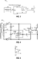
Bei einigen Ausführungsbeispielen bildet die Kombination aus positiver Spannungsquelle 206 und negativer Spannungsquelle 208 eine potentialfreie Leistungsversorgung, deren Gleichtaktspannung durch Anlegen einer Spannung an einem gemeinsamen Knoten 220 eingestellt werden kann, der zwischen die positive Spannungsquelle 206 und die negative Spannungsquelle 208 gekoppelt ist. Durch Koppeln der Spannungsquelle 210 zwischen den gemeinsamen Knoten 220 und den Sourceknoten S des Transistors 202 kann der Gleichtaktausgang der Treiberschaltung 204 entsprechend der zeitabhängigen Einsatzspannung Vth(t) des Transistors 202 oder einer beliebigen anderen zeitabhängigen Spannung eingestellt werden. Bei einigen Ausführungsbeispielen, bei denen die Ausgänge der Spannungsquelle 206 und 208 der Einsatzspannung des Transistors 202 nachlaufen (engl.: track), können die Spannung VP der positiven Spannungsquelle 206 und die Spannung VN der negativen Spannungsquelle 208 gewählt werden, ohne dass eine Variation der Einsatzspannung des Transistors 202 berücksichtigt werden muss. Bei solchen Ausführungsbeispielen können die Mindestwerte von VP und VN gemäß einer Schaltdynamik gewählt werden.In some embodiments, the combination of
Beispielsweise werden bei einem Ausführungsbeispiel die Spannungsquellen 206 und 208 jeweils so eingestellt, dass sie etwa 3 V erzeugen, und die Spannungsquelle 210 ist dazu ausgebildet, eine Spannung zu liefern, die sich der Einsatzspannung des Transistors 202 annähert. Falls die Approximation der Einsatzspannung des Transistors 202 etwa -5 V beträgt, liefert die Spannungsquelle 210 somit etwa -5 V, der positive Anschluss der Spannungsquelle 206 liefert etwa -2 V und der negative Anschluss der Spannungsquelle 208 liefert etwa -8 V. Bei alternativen Ausführungsbeispielen können je nach dem bestimmen System und seinen Spezifikationen andere Spannungspegel verwendet werden.For example, in one embodiment,
Die Spannungsquellen 206 und 208 können unter Verwendung von in der Technik bekannten Leistungsschaltungen implementiert werden. Beispielsweise können getaktete Leistungsversorgungen, Spannungsregler, Batterien und andere Leistungsversorgungsschaltungen und -systeme zum Implementieren der Spannungsquelle 206 und 208 verwendet werden. Beispielsweise kann die Spannungsquelle 210 unter Verwendung verschiedener Vorspannungs-Schaltungen und/oder Leistungsversorgungsschaltungen, die in der Technik bekannt sind, implementiert werden. Bei einigen Ausführungsbeispielen kann die Spannungsquelle 210 unter Verwendung einer Kopie des Transistors 202 implementiert werden, um eine Spannung zu erzeugen, die sich der Einsatzspannung Vth des Transistors 202 annähert. Die Treiberschaltung 204 kann unter Verwendung von in der Technik bekannten Treiberschaltungen implementiert werden, wie etwa einem Treiber aus der Familie Infineon EiceDRIVER oder einem Treiber aus der Serie Texas Instruments UCC27x.
Bei einem Ausführungsbeispiel erzeugt die Transistorkopie-Schaltung 306 eine Spannung V(t), die sich der Einsatzspannung des Transistors 202 annähert und/oder zu ihr in Beziehung steht, indem ein Transistor mit einer ähnlichen Struktur und/oder einer ähnlichen Bauelementgeometrie wie der Transistor 202 verwendet wird. Die Spannung V(t) kann über der Zeit variieren, um Änderungen der Einsatzspannung bezüglich Temperatur, Drifteffekten und Änderungen bei anderen Parametern zu verfolgen, die die Einsatzspannung des Transistors und des Kopiebauelements in der Transistorkopie-Schaltung 306 beeinflussen können. Bei alternativen Ausführungsbeispielen kann die Spannung V(t) neben der Transistorkopie-Schaltung 306 durch andere Arten von Schaltungen erzeugt werden.In one embodiment,
Die Treiberschaltung 304 besitzt Versorgungsanschlüsse, die an die Anschlüsse VP und VN der potentialfreien Leistungsversorgung 302 gekoppelt sind. Bei einem Ausführungsbeispiel legt die Treiberschaltung abwechselnd die Spannungen an den Anschlüssen VP und VN der potentialfreien Leistungsversorgung 302 gemäß einem Schaltsignal am Eingang VSW der Treiberschaltung 304 an den Gateanschluss G des Transistors 202 an. Beispielsweise legt bei einem Ausführungsbeispiel die Treiberschaltung 304 die Spannung am Anschluss VP der potentialfreien Leistungsversorgung 302 an, wenn das Signal am Eingang VSW ein logisches H ist, und legt die Spannung am Anschluss VN der potentialfreien Leistungsversorgung 302 an, wenn das Signal am Eingang VSW ein logisches L ist. Alternativ kann die Beziehung zwischen dem logischen Sinn des Eingangs VSW und der an die Gateelektrode des Transistors 202 angelegten Spannung umgedreht werden. Bei einigen Ausführungsbeispielen kann der Ausgang der Treiberschaltung 304 zwischen seinen Leistungsversorgungsverbindungen und seinem Ausgangsanschluss einen Spannungsabfall einführen.
Das Schalteransteuersystem 400 umfasst den Transistor 202 und die Ansteuerschaltung 402, die dazu ausgebildet ist, ein Schaltsignal VSW an die Gateelektrode des Transistors 202 anzulegen. Der Transistor 202 kann eine beliebige Art von Transistor sein, der beispielsweise eine positive Einsatzspannung oder eine negative Einsatzspannung besitzt. Der positive Leistungsversorgungsanschluss 422 der Treiberschaltung 402 ist über eine Diode 410 an die Wicklung 416 des Transformators 414 gekoppelt und der negative Leistungsversorgungsanschluss 424 der Treiberschaltung 402 ist über die Diode 412 an die Wicklung 418 des Transformators 414 gekoppelt. Die Dioden 410 und 412 richten den Strom in den Wicklungen 416 und 418 des Transformators 414 gleich. Bei einigen Ausführungsbeispielen können die Dioden 410 und 412 unter Verwendung von Schalttransistoren implementiert werden, die als Synchrongleichrichter betrieben werden. Die an die Dioden 410 und 412 gekoppelten Kondensatoren 406 und 408 sorgen für eine Filterung und dämpfen die Versorgungswelligkeit.The
Ein Pufferverstärker 404 mit einer Verstärkung von Eins (engl.: unity gain buffer amplifier) ist dazu ausgebildet, die Spannung V(t) zum Mittenabgriff 432 des Transformators 414 zu puffern. Die Spannung V(t) kann beispielsweise eine Spannung darstellen, die sich der Einsatzspannung des Transistors 202 annähert. Alternativ kann die Spannung V(t) eine beliebige zeitabhängige Spannung sein. Bei vielen Ausführungsbeispielen ist die zeitliche Variation von V(t) langsam im Vergleich zu den Schalttransienten. Dann blockiert der Kondensator C, der zwischen den Sourceknoten S des Transistors 202 und den Ausgang des Pufferverstärkers 404 mit einer Verstärkung von Eins gekoppelt ist, die Gleichtaktversorgungskomponente V(t), liefert aber einen Pfad mit niedriger Impedanz für die schnellen Schalttransienten.A unity
Der Verstärker 404, der in einer Rückkopplungskonfiguration mit Verstärkung Eins (engl.: unity gain feedback configuration) gezeigt ist, kann unter Verwendung eines Transkonduktanzverstärkers, eines Operationsverstärkers oder einer anderen, in der Technik bekannten Art von Verstärker realisiert werden. Bei alternativen Ausführungsbeispielen können andere Verstärkerkonfigurationen neben einer Eins-Konfiguration verwendet werden. Beispielsweise kann ein Verstärker mit einem Leistungsfaktor kleiner eins oder größer als eins verwendet werden. Bei einigen Ausführungsbeispielen kann der Verstärker 404 entfallen. Es versteht sich, dass das System 400 nur eines von vielen Ausführungsbeispielen ist, die verwendet werden können, um ein Ausführungsbeispiel von Transistoransteuerschaltungen und -systemen zu implementieren. Bei alternativen Ausführungsbeispielen können andere Schaltungsarchitekturen und -topologien verwendet werden.
Bei einem Ausführungsbeispiel besitzt der Kopietransistor 508 eine ähnliche Struktur wie der angesteuerte Schalttransistor. Falls beispielsweise der Schalttransistor ein GaN-HEMT ist, ist auch der Kopietransistor 508 ein GaN-HEMT. Bei einigen Ausführungsbeispielen kann auch die Geometrie des Kopietransistors der Geometrie des Schalttransistors entsprechen. Beispielsweise kann der Schalttransistor unter Verwendung von n Einheitsbauelementen konstruiert werden, während der Kopietransistor unter Verwendung von einem oder von zwei des Einheitsbauelements realisiert werden kann. Bei solchen Ausführungsbeispielen muss der Strom der Stromquelle 504 nur in der Größenordnung von 1/n des Stroms des Schalttransistors liegen, damit V(t) die Einsatzspannung des Schalttransistors verfolgen kann. Bei einigen Ausführungsbeispielen können sich die Einheitsbauelemente des Kopietransistors 508 an der gleichen Stelle wie der Schalttransistor befinden, um eine angepasste Leistung zu verbessern. Durch Anordnen des Kopietransistors 508 am gleichen Ort wie dem Hauptschalttransistor werden Änderungen bei der Temperatur beim Schalttransistor auf den Kopietransistor 508 angewendet.In one embodiment,
Es versteht sich, dass die Schaltung von
Gemäß einem Ausführungsbeispiel umfasst eine Schaltung zum Ansteuern eines Steueranschlusses eines Schalttransistors: einen Treiber mit einem Ausgang, der dazu ausgebildet ist, mit einem Steueranschluss des Schalttransistors gekoppelt zu werden, einen ersten Leistungsversorgungsanschluss, der dazu ausgebildet ist, mit einem ersten Anschluss einer potentialfreien Leistungsversorgung gekoppelt zu werden, einen zweiten Leistungsversorgungsanschluss, der dazu ausgebildet ist, mit einem zweiten Anschluss der potentialfreien Leistungsversorgung gekoppelt zu werden, und einen Schalteingangsanschluss, der dazu ausgebildet ist, ein Schaltsignal zu empfangen. Die Schaltung umfasst weiterhin eine Vorspannungs-Schaltung mit einem Ausgangsanschluss, der dazu ausgebildet ist, mit einem Gleichtaktsteueranschluss der potentialfreien Leistungsversorgung gekoppelt zu werden, wobei die Vorspannungs-Schaltung dazu ausgebildet ist, eine zeitabhängige Spannung zu liefern. Bei einigen Ausführungsbeispielen umfasst die Schaltung weiterhin die potentialfreie Leistungsversorgung.According to one embodiment, a circuit for driving a control terminal of a switching transistor includes: a driver having an output configured to be coupled to a control terminal of the switching transistor, a first power supply terminal configured to be coupled to a first terminal of a floating power supply a second power supply terminal configured to be coupled to a second terminal of the floating power supply, and a switch input terminal configured to receive a switch signal. The circuit further includes a bias circuit having an output terminal configured to be coupled to a common mode control terminal of the floating power supply, the bias circuit configured to do so det is to provide a time dependent voltage. In some embodiments, the circuit further includes the floating power supply.
Bei einem Ausführungsbeispiel umfasst die potentialfreie Leistungsversorgung eine erste Spule, eine erste Diode, die zwischen den ersten Anschluss der potentialfreien Leistungsversorgung und die erste Spule gekoppelt ist, eine zweite Spule, die an die erste Spule an dem Gleichtaktsteueranschluss und an den zweiten Anschluss der potentialfreien Leistungsversorgung gekoppelt ist, und eine zweite Diode, die zwischen die zweite Spule und den zweiten Anschluss der potentialfreien Leistungsversorgung gekoppelt ist. Die zweite Spule ist magnetisch an die erste Spule gekoppelt.In one embodiment, the floating power supply includes a first coil, a first diode coupled between the first terminal of the floating power supply and the first coil, a second coil coupled to the first coil at the common mode control terminal, and to the second terminal of the floating power supply and a second diode coupled between the second coil and the second terminal of the floating power supply. The second coil is magnetically coupled to the first coil.
Bei einem Ausführungsbeispiel beinhaltet der Schalttransistor einen selbstleitenden Transistor, der Teil der Schaltung sein kann. Der selbstleitende Transistor kann unter Verwendung eines GaN-HEMT-Bauelements implementiert werden, und der Steueranschluss des selbstleitenden Transistors kann eine Gateelektrode des GaN-HEMT sein. Bei einigen Ausführungsbeispielen ist die zeitabhängige Spannung eine auf einer Einsatzspannung des Schalttransistors basierende Spannung. Diese Spannung kann auf der Einsatzspannung des Schalttransistors basieren und kann eine Spannung sein, die im Wesentlichen gleich der Einsatzspannung des Schalttransistors ist. Bei einem Ausführungsbeispiel besitzt die Bias-Schaltung eine Kopie des Schalttransistors.In one embodiment, the switching transistor includes a normally-on transistor, which may be part of the circuit. The normally on transistor can be implemented using a GaN HEMT device and the control terminal of the normally on transistor can be a gate electrode of the GaN HEMT. In some embodiments, the time-varying voltage is a voltage based on a threshold voltage of the switching transistor. This voltage may be based on the threshold voltage of the switching transistor and may be a voltage substantially equal to the threshold voltage of the switching transistor. In one embodiment, the bias circuit has a copy of the switching transistor.
Bei einem Ausführungsbeispiel ist der Treiber dazu ausgebildet, den Schalttransistor durch Koppeln einer Spannung des ersten Leistungsversorgungsanschlusses an den Steueranschluss des Transistors einzuschalten, und den Schalttransistor durch Koppeln einer Spannung des zweiten Leistungsversorgungsanschlusses an den Steueranschluss des Schalttransistors auszuschalten.In one embodiment, the driver is configured to turn on the switching transistor by coupling a voltage of the first power supply terminal to the control terminal of the transistor and to turn off the switching transistor by coupling a voltage of the second power supply terminal to the control terminal of the switching transistor.
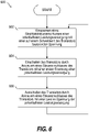
Gemäß einem weiteren Ausführungsbeispiel beinhaltet ein Verfahren zum Steuern eines Schalttransistors: Einschalten des Schalttransistors durch Ansteuern eines Steueranschlusses des Schalttransistors mit einer ersten Spannung einer potentialfreien Leistungsversorgung, Ausschalten des Schalttransistors durch Ansteuern eines Steueranschlusses des Schalttransistors mit einer zweiten Spannung der potentialfreien Leistungsversorgung, und Vorspannen eines Gleichtaktsteueranschlusses der potentialfreien Leistungsversorgung mit einer auf einer Einsatzspannung des Schalttransistors basierenden Spannung, die im Wesentlichen gleich der Einsatzspannung des Schalttransistors sein kann. Das Vorspannen des Gleichtaktsteueranschlusses der potentialfreien Leistungsversorgung kann das Bereitstellen einer Einsatzspannung einer Kopie des Schalttransistors beinhalten.According to another embodiment, a method of controlling a switching transistor includes: turning on the switching transistor by driving a control terminal of the switching transistor with a first floating power supply voltage, turning off the switching transistor by driving a control terminal of the switching transistor with a second floating power supply voltage, and biasing a common mode control terminal the floating power supply with a voltage based on a threshold voltage of the switching transistor, which may be substantially equal to the threshold voltage of the switching transistor. Biasing the common mode control terminal of the floating power supply may include providing a turn-on voltage to a copy of the switching transistor.
Bei einem Ausführungsbeispiel werden die Schritte des Einschaltens und Ausschaltens gemäß einem Schaltsignal durchgeführt. Der Schalttransistor kann einen selbstleitenden Transistor beinhalten, und der Schalttransistor beinhaltet ein GaN-HEMT-Bauelement, so dass der Steueranschluss des Schalttransistors eine Gateelektrode des GaN-HEMT ist.In one embodiment, the steps of turning on and off are performed according to a switching signal. The switching transistor may include a normally-on transistor, and the switching transistor includes a GaN HEMT device such that the control terminal of the switching transistor is a gate electrode of the GaN HEMT.
Gemäß einem weiteren Ausführungsbeispiel umfasst ein Schaltkreis eine potentialfreie Leistungsversorgung mit einem positiven Anschluss, einem negativen Anschluss und einem Gleichtaktanschluss. Der Schaltkreis umfasst weiterhin eine Treiberschaltung mit einem ersten Leistungsversorgungsanschluss, der an den positiven Anschluss der Leistungsversorgung gekoppelt ist, einem zweiten Leistungsversorgungsanschluss, der an den negativen Anschluss der Leistungsversorgung gekoppelt ist, und einem Ausgangsanschluss, der dazu ausgebildet ist, mit einem Steueranschluss eines Schalttransistors gekoppelt zu werden. Der Schaltkreis umfasst weiterhin eine Gleichtakt-Bias-Schaltung mit einem Ausgang, der an den Gleichtaktanschluss der potentialfreien Leistungsversorgung gekoppelt ist, so dass die Gleichtakt-Bias-Schaltung dazu ausgebildet ist, eine auf einer Einsatzspannung des Schalttransistors basierenden Spannung am Ausgang der Gleichtakt-Bias-Spannung bereitzustellen. Bei einigen Ausführungsbeispielen umfasst der Schaltkreis den Schalttransistor.According to another embodiment, a circuit includes a floating power supply having a positive terminal, a negative terminal, and a common mode terminal. The circuit further includes a driver circuit having a first power supply terminal coupled to the positive terminal of the power supply, a second power supply terminal coupled to the negative terminal of the power supply, and an output terminal configured to be coupled to a control terminal of a switching transistor to become. The circuit further includes a common mode bias circuit having an output coupled to the common mode terminal of the floating power supply, such that the common mode bias circuit is configured to output a voltage based on a threshold voltage of the switching transistor at the output of the common mode bias - Provide tension. In some embodiments, the switching circuit includes the switching transistor.
Bei einem Ausführungsbeispiel beinhaltet der Schalttransistor einen selbstleitenden Transistor, und der selbstleitende Transistor beinhaltet ein GaN-HEMT-Bauelement, so dass der Steueranschluss des Schalttransistors eine Gateelektrode des GaN-HEMT umfasst. Die Gleichtakt-Bias-Schaltung kann einen Spannungspufferverstärker mit einem Ausgang enthalten, der an den Gleichtaktanschluss der potentialfreien Leistungsversorgung gekoppelt ist.In one embodiment, the switching transistor includes a normally on transistor and the normally on transistor includes a GaN HEMT device such that the control terminal of the switching transistor includes a gate electrode of the GaN HEMT. The common mode bias circuit may include a voltage buffer amplifier having an output coupled to the common mode terminal of the floating power supply.
Die Schalt-Schaltung kann einen Kondensator enthalten, der zwischen einem Lastweganschluss des Schalttransistors und den Ausgang des Spannungspufferverstärkers gekoppelt ist, und kann auch einen Kopietransistor enthalten, der mit einem Eingang des Spannungspufferverstärkers gekoppelt ist. Bei einigen Ausführungsbeispielen umfasst die potentialfreie Leistungsversorgung einen Transformator, und der Gleichtaktanschluss der potentialfreien Leistungsversorgung umfasst einen Mittenabgriffsanschluss des Transformators.The switching circuit may include a capacitor coupled between a load path terminal of the switching transistor and the output of the voltage buffer amplifier, and may also include a copy transistor coupled to an input of the voltage buffer amplifier. In some embodiments, the floating power supply includes a transformer, and the common mode terminal of the floating power supply includes a center-tapped terminal of the transformer.
Zu Vorteilen einiger Ausführungsbeispiele zählen Leistungseinsparungen aufgrund dessen, dass niedrigere Versorgungsspannungen verwendet werden, um Leistung an Schalttreiber zu liefern. Ein weiterer Vorteil beinhaltet die Fähigkeit zum Verfolgen der Einsatzspannungsvariation über die Zeit und die Fähigkeit zum Liefern symmetrischer Ansteuerspannungen an Schalttransistoren.Advantages of some embodiments include power savings due to using lower supply voltages be used to deliver power to switching drivers. Another advantage includes the ability to track threshold voltage variation over time and the ability to provide symmetrical drive voltages to switching transistors.
Zu weiteren Vorteilen der Ausführungsbeispiele zählt die Fähigkeit zum Variieren der Gateansteuerpegel nicht nur bezüglich der Transistor-Einsatzspannung, sondern auch zum Berücksichtigen anderer Aspekte wie etwa den Transistorarbeitsmodus (Schalter/Diode), die Laststromvariation und die Schaltgeschwindigkeit.Other advantages of the embodiments include the ability to vary gate drive levels not only in terms of transistor threshold voltage, but also to account for other aspects such as transistor operating mode (switch/diode), load current variation, and switching speed.
Claims (23)
Applications Claiming Priority (2)
| Application Number | Priority Date | Filing Date | Title |
|---|---|---|---|
| US14/473,300 | 2014-08-29 | ||
| US14/473,300 US9467061B2 (en) | 2014-08-29 | 2014-08-29 | System and method for driving a transistor |
Publications (2)
| Publication Number | Publication Date |
|---|---|
| DE102015114366A1 DE102015114366A1 (en) | 2016-03-03 |
| DE102015114366B4 true DE102015114366B4 (en) | 2022-06-15 |
Family
ID=55312384
Family Applications (1)
| Application Number | Title | Priority Date | Filing Date |
|---|---|---|---|
| DE102015114366.6A Active DE102015114366B4 (en) | 2014-08-29 | 2015-08-28 | SYSTEM AND METHOD FOR DRIVING A TRANSISTOR |
Country Status (2)
| Country | Link |
|---|---|
| CN (1) | CN105391435B (en) |
| DE (1) | DE102015114366B4 (en) |
Citations (1)
| Publication number | Priority date | Publication date | Assignee | Title |
|---|---|---|---|---|
| DE102011087434A1 (en) | 2010-11-30 | 2012-05-31 | Infineon Technologies Ag | Arrangement and method for driving a switch |
Family Cites Families (6)
| Publication number | Priority date | Publication date | Assignee | Title |
|---|---|---|---|---|
| JP2005304210A (en) * | 2004-04-14 | 2005-10-27 | Renesas Technology Corp | Power supply driver device and switching power supply device |
| US7557644B2 (en) * | 2005-10-07 | 2009-07-07 | International Rectifier Corporation | Fully integrated floating power supply for high voltage technologies including N-EPI biasing |
| US9166533B2 (en) * | 2009-07-30 | 2015-10-20 | Qualcomm Incorporated | Bias current monitor and control mechanism for amplifiers |
| US8779745B2 (en) * | 2010-03-01 | 2014-07-15 | National Semiconductor Corporation | Three-quarter bridge power converters for wireless power transfer applications and other applications |
| US8558584B2 (en) * | 2010-11-30 | 2013-10-15 | Infineon Technologies Ag | System and method for bootstrapping a switch driver |
| CN103931081B (en) * | 2011-06-10 | 2018-11-13 | 艾克西弗拉克斯控股有限公司 | Motor/generator |
-
2015
- 2015-08-28 DE DE102015114366.6A patent/DE102015114366B4/en active Active
- 2015-08-28 CN CN201510541542.4A patent/CN105391435B/en active Active
Patent Citations (1)
| Publication number | Priority date | Publication date | Assignee | Title |
|---|---|---|---|---|
| DE102011087434A1 (en) | 2010-11-30 | 2012-05-31 | Infineon Technologies Ag | Arrangement and method for driving a switch |
Also Published As
| Publication number | Publication date |
|---|---|
| CN105391435B (en) | 2018-08-10 |
| CN105391435A (en) | 2016-03-09 |
| DE102015114366A1 (en) | 2016-03-03 |
Similar Documents
| Publication | Publication Date | Title |
|---|---|---|
| DE102015114365B4 (en) | SYSTEM AND METHOD FOR GENERATION OF AN AUXILIARY VOLTAGE | |
| DE102016114820B4 (en) | System and method for a switch having a normally-on transistor and a normally-off transistor | |
| DE102015114371B4 (en) | SYSTEM AND METHOD FOR A SWITCH WITH A SELF-ONING TRANSISTOR AND A SELF-OFF TRANSISTOR | |
| DE102015114373B4 (en) | SYSTEM AND PROCEDURE FOR A SWITCH WITH A SELF-CONDUCTING TRANSISTOR AND A SELF-LOCKING TRANSISTOR | |
| DE112017006120B4 (en) | BOOTSTRAP CAPACITOR OVERVOLTAGE MONITORING CIRCUIT FOR CONVERTERS BASED ON GAN TRANSISTORS | |
| DE102018126779B4 (en) | Gate driver circuit with voltage inversion for a power semiconductor switch | |
| DE102015104946B4 (en) | Electronic driver circuit and method | |
| DE102011087434B4 (en) | Circuit and three methods of driving a switch | |
| DE102013219472B4 (en) | SWITCHING CIRCUIT WITH A FIRST TRANSISTOR CONSTRUCTION ELEMENT AND A SECOND TRANSISTOR COMPONENT SWITCHED IN SERIES | |
| DE102014118167B4 (en) | Analog switches and methods of controlling analog switches | |
| DE112012001674T5 (en) | Cascade switch with self-locking and normally-on components and circuits comprising the switches | |
| DE102013219475B4 (en) | ELECTRONIC CIRCUIT WITH AN ELECTRONIC SWITCH AND A MONITORING CIRCUIT | |
| DE112017003652T5 (en) | Hybrid switch with GaN HEMT and MOSFET | |
| DE102019102311A1 (en) | Gate driver circuit with voltage inversion for a power semiconductor switch | |
| DE102006029474A1 (en) | Cascode circuit for driving high electron mobility transistor, has controller that controls low voltage MOSFET for faster charging of capacitor | |
| EP0060336A2 (en) | Method of driving a power FET switching transistor and circuit arrangements for carrying out this method | |
| DE102014107815A1 (en) | System and method for driving transistors | |
| DE102019104691B4 (en) | diode circuit | |
| DE102016103130B4 (en) | Circuit arrangement with a rectifier circuit and method | |
| DE102016110021A1 (en) | System and method for a gate driver | |
| DE102015109948A1 (en) | System and method for a normally-switched switched-mode power supply | |
| DE102015101975A1 (en) | Electronic circuit operable as an electronic switch | |
| WO2015117691A1 (en) | Rectifier circuit with self-clamping transistor | |
| DE102017101272A1 (en) | Driver for a high-side switch of a cascode switch | |
| EP3316463A1 (en) | Change in the switching state of a switching half bridge |
Legal Events
| Date | Code | Title | Description |
|---|---|---|---|
| R012 | Request for examination validly filed | ||
| R016 | Response to examination communication | ||
| R018 | Grant decision by examination section/examining division | ||
| R020 | Patent grant now final | ||
| R082 | Change of representative |