DE102008052595B4 - A method of fabricating a semiconductor device as a high electron mobility semiconductor device (HEMT) having a field weakening plate and semiconductor device - Google Patents
A method of fabricating a semiconductor device as a high electron mobility semiconductor device (HEMT) having a field weakening plate and semiconductor device Download PDFInfo
- Publication number
- DE102008052595B4 DE102008052595B4 DE102008052595A DE102008052595A DE102008052595B4 DE 102008052595 B4 DE102008052595 B4 DE 102008052595B4 DE 102008052595 A DE102008052595 A DE 102008052595A DE 102008052595 A DE102008052595 A DE 102008052595A DE 102008052595 B4 DE102008052595 B4 DE 102008052595B4
- Authority
- DE
- Germany
- Prior art keywords
- layer
- gate
- forming
- field plate
- semiconductor device
- Prior art date
- Legal status (The legal status is an assumption and is not a legal conclusion. Google has not performed a legal analysis and makes no representation as to the accuracy of the status listed.)
- Active
Links
- 239000004065 semiconductor Substances 0.000 title claims abstract description 69
- 238000004519 manufacturing process Methods 0.000 title description 12
- 230000003313 weakening effect Effects 0.000 title description 11
- 238000000034 method Methods 0.000 claims abstract description 37
- 239000000758 substrate Substances 0.000 claims abstract description 35
- 229910052751 metal Inorganic materials 0.000 claims abstract description 30
- 239000002184 metal Substances 0.000 claims abstract description 30
- 238000000151 deposition Methods 0.000 claims abstract description 17
- 239000004922 lacquer Substances 0.000 claims abstract description 16
- 230000004888 barrier function Effects 0.000 claims description 29
- 239000003973 paint Substances 0.000 claims description 23
- 229910052581 Si3N4 Inorganic materials 0.000 claims description 15
- HQVNEWCFYHHQES-UHFFFAOYSA-N silicon nitride Chemical compound N12[Si]34N5[Si]62N3[Si]51N64 HQVNEWCFYHHQES-UHFFFAOYSA-N 0.000 claims description 15
- 230000005684 electric field Effects 0.000 claims description 12
- 239000003989 dielectric material Substances 0.000 claims description 7
- 238000001459 lithography Methods 0.000 claims description 7
- 230000008021 deposition Effects 0.000 claims description 6
- 238000000623 plasma-assisted chemical vapour deposition Methods 0.000 claims description 5
- 230000015572 biosynthetic process Effects 0.000 claims description 3
- 238000000609 electron-beam lithography Methods 0.000 claims description 3
- 150000001875 compounds Chemical class 0.000 claims description 2
- 238000001451 molecular beam epitaxy Methods 0.000 claims description 2
- 239000011248 coating agent Substances 0.000 claims 1
- 238000000576 coating method Methods 0.000 claims 1
- 230000008569 process Effects 0.000 abstract description 13
- PXHVJJICTQNCMI-UHFFFAOYSA-N Nickel Chemical compound [Ni] PXHVJJICTQNCMI-UHFFFAOYSA-N 0.000 description 7
- 230000015556 catabolic process Effects 0.000 description 6
- 238000010586 diagram Methods 0.000 description 5
- 229920003229 poly(methyl methacrylate) Polymers 0.000 description 5
- 239000004926 polymethyl methacrylate Substances 0.000 description 5
- PIGFYZPCRLYGLF-UHFFFAOYSA-N Aluminum nitride Chemical compound [Al]#N PIGFYZPCRLYGLF-UHFFFAOYSA-N 0.000 description 4
- VYPSYNLAJGMNEJ-UHFFFAOYSA-N Silicium dioxide Chemical compound O=[Si]=O VYPSYNLAJGMNEJ-UHFFFAOYSA-N 0.000 description 4
- 230000008901 benefit Effects 0.000 description 4
- 239000010931 gold Substances 0.000 description 4
- 230000006911 nucleation Effects 0.000 description 4
- 238000010899 nucleation Methods 0.000 description 4
- 238000005389 semiconductor device fabrication Methods 0.000 description 4
- HBMJWWWQQXIZIP-UHFFFAOYSA-N silicon carbide Chemical compound [Si+]#[C-] HBMJWWWQQXIZIP-UHFFFAOYSA-N 0.000 description 4
- ZWEHNKRNPOVVGH-UHFFFAOYSA-N 2-Butanone Chemical compound CCC(C)=O ZWEHNKRNPOVVGH-UHFFFAOYSA-N 0.000 description 3
- KDLHZDBZIXYQEI-UHFFFAOYSA-N Palladium Chemical compound [Pd] KDLHZDBZIXYQEI-UHFFFAOYSA-N 0.000 description 3
- 229920001577 copolymer Polymers 0.000 description 3
- 238000006731 degradation reaction Methods 0.000 description 3
- 238000010894 electron beam technology Methods 0.000 description 3
- PCHJSUWPFVWCPO-UHFFFAOYSA-N gold Chemical compound [Au] PCHJSUWPFVWCPO-UHFFFAOYSA-N 0.000 description 3
- 229910052737 gold Inorganic materials 0.000 description 3
- 229910052759 nickel Inorganic materials 0.000 description 3
- 150000004767 nitrides Chemical class 0.000 description 3
- BASFCYQUMIYNBI-UHFFFAOYSA-N platinum Chemical compound [Pt] BASFCYQUMIYNBI-UHFFFAOYSA-N 0.000 description 3
- 238000001878 scanning electron micrograph Methods 0.000 description 3
- 229910010271 silicon carbide Inorganic materials 0.000 description 3
- 239000010936 titanium Substances 0.000 description 3
- CSCPPACGZOOCGX-UHFFFAOYSA-N Acetone Chemical compound CC(C)=O CSCPPACGZOOCGX-UHFFFAOYSA-N 0.000 description 2
- 229910002601 GaN Inorganic materials 0.000 description 2
- JMASRVWKEDWRBT-UHFFFAOYSA-N Gallium nitride Chemical compound [Ga]#N JMASRVWKEDWRBT-UHFFFAOYSA-N 0.000 description 2
- 229910004298 SiO 2 Inorganic materials 0.000 description 2
- RTAQQCXQSZGOHL-UHFFFAOYSA-N Titanium Chemical compound [Ti] RTAQQCXQSZGOHL-UHFFFAOYSA-N 0.000 description 2
- 238000013461 design Methods 0.000 description 2
- 230000000694 effects Effects 0.000 description 2
- 238000009616 inductively coupled plasma Methods 0.000 description 2
- 239000000463 material Substances 0.000 description 2
- 230000007246 mechanism Effects 0.000 description 2
- 238000001020 plasma etching Methods 0.000 description 2
- 235000012239 silicon dioxide Nutrition 0.000 description 2
- 239000000377 silicon dioxide Substances 0.000 description 2
- 239000002904 solvent Substances 0.000 description 2
- 229910052719 titanium Inorganic materials 0.000 description 2
- 239000002966 varnish Substances 0.000 description 2
- 229910018072 Al 2 O 3 Inorganic materials 0.000 description 1
- ZOKXTWBITQBERF-UHFFFAOYSA-N Molybdenum Chemical compound [Mo] ZOKXTWBITQBERF-UHFFFAOYSA-N 0.000 description 1
- 229910045601 alloy Inorganic materials 0.000 description 1
- 239000000956 alloy Substances 0.000 description 1
- 229910052782 aluminium Inorganic materials 0.000 description 1
- XAGFODPZIPBFFR-UHFFFAOYSA-N aluminium Chemical compound [Al] XAGFODPZIPBFFR-UHFFFAOYSA-N 0.000 description 1
- RNQKDQAVIXDKAG-UHFFFAOYSA-N aluminum gallium Chemical compound [Al].[Ga] RNQKDQAVIXDKAG-UHFFFAOYSA-N 0.000 description 1
- QVGXLLKOCUKJST-UHFFFAOYSA-N atomic oxygen Chemical compound [O] QVGXLLKOCUKJST-UHFFFAOYSA-N 0.000 description 1
- NWAIGJYBQQYSPW-UHFFFAOYSA-N azanylidyneindigane Chemical compound [In]#N NWAIGJYBQQYSPW-UHFFFAOYSA-N 0.000 description 1
- 230000008859 change Effects 0.000 description 1
- 239000002131 composite material Substances 0.000 description 1
- 230000006835 compression Effects 0.000 description 1
- 238000007906 compression Methods 0.000 description 1
- 238000007796 conventional method Methods 0.000 description 1
- 238000001312 dry etching Methods 0.000 description 1
- 238000005566 electron beam evaporation Methods 0.000 description 1
- 238000005538 encapsulation Methods 0.000 description 1
- 238000005516 engineering process Methods 0.000 description 1
- 238000005530 etching Methods 0.000 description 1
- 230000005669 field effect Effects 0.000 description 1
- -1 for example Substances 0.000 description 1
- 230000006872 improvement Effects 0.000 description 1
- 239000011810 insulating material Substances 0.000 description 1
- 239000012212 insulator Substances 0.000 description 1
- 239000007788 liquid Substances 0.000 description 1
- 238000005259 measurement Methods 0.000 description 1
- 150000002739 metals Chemical class 0.000 description 1
- 229910052750 molybdenum Inorganic materials 0.000 description 1
- 239000011733 molybdenum Substances 0.000 description 1
- 230000001590 oxidative effect Effects 0.000 description 1
- TWNQGVIAIRXVLR-UHFFFAOYSA-N oxo(oxoalumanyloxy)alumane Chemical compound O=[Al]O[Al]=O TWNQGVIAIRXVLR-UHFFFAOYSA-N 0.000 description 1
- 239000001301 oxygen Substances 0.000 description 1
- 229910052760 oxygen Inorganic materials 0.000 description 1
- 229910052763 palladium Inorganic materials 0.000 description 1
- 230000003071 parasitic effect Effects 0.000 description 1
- 238000002161 passivation Methods 0.000 description 1
- 238000000059 patterning Methods 0.000 description 1
- 238000000206 photolithography Methods 0.000 description 1
- 229920002120 photoresistant polymer Polymers 0.000 description 1
- 229910052697 platinum Inorganic materials 0.000 description 1
- 238000012545 processing Methods 0.000 description 1
- 230000009467 reduction Effects 0.000 description 1
- 230000035945 sensitivity Effects 0.000 description 1
- 238000000926 separation method Methods 0.000 description 1
- 238000004544 sputter deposition Methods 0.000 description 1
- 239000000126 substance Substances 0.000 description 1
- WFKWXMTUELFFGS-UHFFFAOYSA-N tungsten Chemical compound [W] WFKWXMTUELFFGS-UHFFFAOYSA-N 0.000 description 1
- 229910052721 tungsten Inorganic materials 0.000 description 1
- 239000010937 tungsten Substances 0.000 description 1
- 230000005533 two-dimensional electron gas Effects 0.000 description 1
- 238000007740 vapor deposition Methods 0.000 description 1
- 238000005019 vapor deposition process Methods 0.000 description 1
- 238000009834 vaporization Methods 0.000 description 1
- 230000008016 vaporization Effects 0.000 description 1
- 238000001039 wet etching Methods 0.000 description 1
Images


Classifications
-
- H—ELECTRICITY
- H01—ELECTRIC ELEMENTS
- H01L—SEMICONDUCTOR DEVICES NOT COVERED BY CLASS H10
- H01L29/00—Semiconductor devices adapted for rectifying, amplifying, oscillating or switching, or capacitors or resistors with at least one potential-jump barrier or surface barrier, e.g. PN junction depletion layer or carrier concentration layer; Details of semiconductor bodies or of electrodes thereof ; Multistep manufacturing processes therefor
- H01L29/66—Types of semiconductor device ; Multistep manufacturing processes therefor
- H01L29/68—Types of semiconductor device ; Multistep manufacturing processes therefor controllable by only the electric current supplied, or only the electric potential applied, to an electrode which does not carry the current to be rectified, amplified or switched
- H01L29/76—Unipolar devices, e.g. field effect transistors
- H01L29/772—Field effect transistors
- H01L29/778—Field effect transistors with two-dimensional charge carrier gas channel, e.g. HEMT ; with two-dimensional charge-carrier layer formed at a heterojunction interface
- H01L29/7786—Field effect transistors with two-dimensional charge carrier gas channel, e.g. HEMT ; with two-dimensional charge-carrier layer formed at a heterojunction interface with direct single heterostructure, i.e. with wide bandgap layer formed on top of active layer, e.g. direct single heterostructure MIS-like HEMT
-
- H—ELECTRICITY
- H01—ELECTRIC ELEMENTS
- H01L—SEMICONDUCTOR DEVICES NOT COVERED BY CLASS H10
- H01L29/00—Semiconductor devices adapted for rectifying, amplifying, oscillating or switching, or capacitors or resistors with at least one potential-jump barrier or surface barrier, e.g. PN junction depletion layer or carrier concentration layer; Details of semiconductor bodies or of electrodes thereof ; Multistep manufacturing processes therefor
- H01L29/40—Electrodes ; Multistep manufacturing processes therefor
- H01L29/402—Field plates
- H01L29/404—Multiple field plate structures
-
- H—ELECTRICITY
- H01—ELECTRIC ELEMENTS
- H01L—SEMICONDUCTOR DEVICES NOT COVERED BY CLASS H10
- H01L29/00—Semiconductor devices adapted for rectifying, amplifying, oscillating or switching, or capacitors or resistors with at least one potential-jump barrier or surface barrier, e.g. PN junction depletion layer or carrier concentration layer; Details of semiconductor bodies or of electrodes thereof ; Multistep manufacturing processes therefor
- H01L29/66—Types of semiconductor device ; Multistep manufacturing processes therefor
- H01L29/66007—Multistep manufacturing processes
- H01L29/66075—Multistep manufacturing processes of devices having semiconductor bodies comprising group 14 or group 13/15 materials
- H01L29/66227—Multistep manufacturing processes of devices having semiconductor bodies comprising group 14 or group 13/15 materials the devices being controllable only by the electric current supplied or the electric potential applied, to an electrode which does not carry the current to be rectified, amplified or switched, e.g. three-terminal devices
- H01L29/66409—Unipolar field-effect transistors
- H01L29/66446—Unipolar field-effect transistors with an active layer made of a group 13/15 material, e.g. group 13/15 velocity modulation transistor [VMT], group 13/15 negative resistance FET [NERFET]
- H01L29/66462—Unipolar field-effect transistors with an active layer made of a group 13/15 material, e.g. group 13/15 velocity modulation transistor [VMT], group 13/15 negative resistance FET [NERFET] with a heterojunction interface channel or gate, e.g. HFET, HIGFET, SISFET, HJFET, HEMT
-
- H—ELECTRICITY
- H01—ELECTRIC ELEMENTS
- H01L—SEMICONDUCTOR DEVICES NOT COVERED BY CLASS H10
- H01L29/00—Semiconductor devices adapted for rectifying, amplifying, oscillating or switching, or capacitors or resistors with at least one potential-jump barrier or surface barrier, e.g. PN junction depletion layer or carrier concentration layer; Details of semiconductor bodies or of electrodes thereof ; Multistep manufacturing processes therefor
- H01L29/66—Types of semiconductor device ; Multistep manufacturing processes therefor
- H01L29/68—Types of semiconductor device ; Multistep manufacturing processes therefor controllable by only the electric current supplied, or only the electric potential applied, to an electrode which does not carry the current to be rectified, amplified or switched
- H01L29/76—Unipolar devices, e.g. field effect transistors
- H01L29/772—Field effect transistors
- H01L29/778—Field effect transistors with two-dimensional charge carrier gas channel, e.g. HEMT ; with two-dimensional charge-carrier layer formed at a heterojunction interface
- H01L29/7782—Field effect transistors with two-dimensional charge carrier gas channel, e.g. HEMT ; with two-dimensional charge-carrier layer formed at a heterojunction interface with confinement of carriers by at least two heterojunctions, e.g. DHHEMT, quantum well HEMT, DHMODFET
- H01L29/7783—Field effect transistors with two-dimensional charge carrier gas channel, e.g. HEMT ; with two-dimensional charge-carrier layer formed at a heterojunction interface with confinement of carriers by at least two heterojunctions, e.g. DHHEMT, quantum well HEMT, DHMODFET using III-V semiconductor material
-
- H—ELECTRICITY
- H01—ELECTRIC ELEMENTS
- H01L—SEMICONDUCTOR DEVICES NOT COVERED BY CLASS H10
- H01L29/00—Semiconductor devices adapted for rectifying, amplifying, oscillating or switching, or capacitors or resistors with at least one potential-jump barrier or surface barrier, e.g. PN junction depletion layer or carrier concentration layer; Details of semiconductor bodies or of electrodes thereof ; Multistep manufacturing processes therefor
- H01L29/02—Semiconductor bodies ; Multistep manufacturing processes therefor
- H01L29/12—Semiconductor bodies ; Multistep manufacturing processes therefor characterised by the materials of which they are formed
- H01L29/20—Semiconductor bodies ; Multistep manufacturing processes therefor characterised by the materials of which they are formed including, apart from doping materials or other impurities, only AIIIBV compounds
- H01L29/2003—Nitride compounds
Abstract
Verfahren zum Ausbilden eines Halbleiterbauelements auf einem Halbleitersubstrat (100), wobei das Halbleitersubstrat (100) ein Sourcegebiet (104), ein Draingebiet (102) und ein T-Gate (111) enthält, wobei das Verfahren folgendes umfasst:
– Ausbilden einer Lackschicht (114) auf dem Halbleitersubstrat (100);
– Ausbilden eines Fensters (116) in der Lackschicht (114);
– Abscheiden eines Metallfilms (118) durch eine Technik einer gerichteten Abscheidung in dem Fenster (116) und auf der Lackschicht (114) und
– Abheben der Lackschicht (114) zum Ausbilden einer ersten, über einem Abschnitt des T-Gate (111) angeordneten Feldplatte (120), und einer zweiten, auf dem Halbleitersubstrat (100) und in einer Nähe des T-Gate (111) angeordneten Feldplatte (122).A method of forming a semiconductor device on a semiconductor substrate (100), the semiconductor substrate (100) including a source region (104), a drain region (102), and a T-gate (111), the process comprising:
- forming a resist layer (114) on the semiconductor substrate (100);
- forming a window (116) in the lacquer layer (114);
Depositing a metal film (118) by a directional deposition technique in the window (116) and on the lacquer layer (114) and
- raising the lacquer layer (114) to form a first field plate (120) arranged above a section of the T-gate (111), and a second, arranged on the semiconductor substrate (100) and in the vicinity of the T-gate (111) Field plate (122).

Description
ERFINDUNGSGEBIETFIELD OF THE INVENTION
Das Erfindungsgebiet betrifft allgemein ein Halbleiterbauelement und ein Fabrikationsverfahren zu dessen Herstellung und insbesondere ein Halbleiterbauelement, das bei Mikrowellen- und Millimeterwellenfrequenzen arbeitet.The invention relates generally to a semiconductor device and a fabrication process for the fabrication thereof, and more particularly to a semiconductor device operating at microwave and millimeter wave frequencies.
ALLGEMEINER STAND DER TECHNIKGENERAL PRIOR ART
Halbleiter mit einem großen Bandabstand wie etwa Nitride der Gruppe III bieten eine Reihe von hervorragenden Eigenschaften, die sie für eine Reihe von Elektronikanwendungen sehr attraktiv machen. Insbesondere hohe Durchschlagfestigkeiten für elektrische Felder, hohe Stromführungsfähigkeiten und hohe Elektronensättigungsgeschwindigkeiten gestatten, dass HEMTs (High Electron Mobility Transistors – Transistoren mit hoher Elektronenmobilität) auf Nitridbasis bei Mikrowellen- und Millimeterwellenfrequenzen einen Betrieb bei sehr hoher Spannung und mit sehr hoher Leistung bereitstehen.Large band gap semiconductors, such as Group III nitrides, offer a number of excellent properties that make them very attractive for a range of electronic applications. In particular, high electric field breakdown strengths, high current carrying capabilities, and high electron saturation rates allow HEMTs (High Electron Mobility Transistors) to operate at very high voltage and very high power at nitride-based microwave and millimeter-wave frequencies.
Um die breitskalige Anwendung dieser Technologie zu fördern, müssen Gruppe-III-Nitrid-HEMTs gewissen Metriken wie Mindestarbeitszeitdauer vor einer Leistungsverschlechterung genügen. Ein bestimmter Aspekt, der die Bauelementlebensdauer begrenzt hat, war das Vorliegen von starken elektrischen Feldern in diesen Strukturen, was zu erhöhtem Einfangen von Ladungen und einem übermäßigem Gateleckstrom mit der Beanspruchungszeit führen kann. Diese feldgetriebenen Mechanismen können signifikante Hindernisse darstellen, um eine Bauelementstabilität zu erzielen.To promote the widespread application of this technology, Group III Nitride HEMTs must meet certain metrics such as minimum work time before performance degradation. One particular aspect that has limited device lifetime has been the presence of strong electric fields in these structures, which can result in increased charge trapping and excess gate leakage current with stress time. These field-driven mechanisms can pose significant obstacles to achieving device stability.
Aus der Druckschrift
Es wäre wünschenswert und stellt sich als Aufgabe, einen Halbleiterbauelementfabrikationsprozess zur Verfügung zu stellen, der durch ein starkes elektrisches Feld induzierte Degradationsmechanismen auf ein Minimum reduzieren und die Herstellung von HEMT-Bauelementen ermöglichen könnte, die sich für einen zuverlässigen Mikrowellen- und Millimeterwellenfrequenzbetrieb eignen. Es wäre weiterhin wünschenswert, dass ein derartiger Halbleiterfabrikationsprozess auch der Produktionseffizienz und dem Komplexitätsniveau von gegenwärtigen Halbleiterbauelementfabrikationsprozessen genugen würde. Es wäre weiterhin wünschenswert, dass ein derartiger Halbleiterfabrikationsprozess Wiederholbarkeit und Robustheit in einer Herstellungsumgebung aufweist.It would be desirable and desired to provide a semiconductor device fabrication process that could minimize strong electric field induced degradation mechanisms and enable the fabrication of HEMT devices suitable for reliable microwave and millimeter wave frequency operation. It would further be desirable that such a semiconductor fabrication process also meet the production efficiency and complexity level of current semiconductor device fabrication processes. It would further be desirable for such a semiconductor fabrication process to have repeatability and robustness in a manufacturing environment.
KÜRZE DARSTELLUNG DER ERFINDUNGBRIEF SUMMARY OF THE INVENTION
Dementsprechend enthält ein Halbleiterbauelement gemäß verschiedenen Ausführungsformen eine Feldplatte zum Minimieren der oben beschriebenen elektrischen Felder und zum Verbessern der Bauelementzuverlässigkeit ohne signifikante Beeinflussung der Bauelementleistung bei Millimeterwellenfrequenzen.Accordingly, a semiconductor device according to various embodiments includes a field plate for minimizing the above-described electric fields and improving device reliability without significantly affecting device performance at millimeter wave frequencies.
Ein Verfahren zum Ausbilden des Halbleiterbauelements auf einem Halbleitersubstrat einschließlich einem Sourcegebiet, einem Draingebiet, einem T-Gate und einem feldabschwächenden Merkmal gemäß verschiedenen Ausführungsformen beinhaltet: Ausbilden einer Dielektrikumsschicht über dem T-Gate und eines Oberflächenbereichs zwischen dem T-Gate und dem Sourcegebiet und zwischen dem T-Gate und dem Draingebiet; Ausbilden einer Lackschicht auf der Dielektrikumsschicht; Ausbilden eines Fensters in der Lackschicht; Abscheiden eines Metallfilms durch eine Technik einer gerichteten Abscheidung in dem Fenster und auf der Lackschicht und Abheben der Lackschicht zum Ausbilden einer ersten Feldplatte (elektrisch inaktive oder potentialfreie Feldplatte), die über einem Abschnitt des T-Gate angeordnet ist, und einer zweiten Feldplatte (aktive Feldplatte), die auf dem Halbleitersubstrat und in einer Nähe des T-Gate angeordnet ist.A method of forming the semiconductor device on a semiconductor substrate including a source region, a drain region, a T-gate, and a field weakening feature according to various embodiments includes: forming a dielectric layer over the T-gate and a surface region between the T-gate and the source region and between the T-gate and the drainage area; Forming a resist layer on the dielectric layer; Forming a window in the lacquer layer; Depositing a metal film by a technique of directional deposition in the window and on the resist layer and lifting the resist layer to form a first field plate (electrically inactive or floating field plate) disposed over a portion of the T-gate and a second field plate (active Field plate) disposed on the semiconductor substrate and in proximity to the T-gate.
Gemäß dem neuartigen Verfahren kann die Feldplattengeometrie optimiert werden. Insbesondere kann eine präzise Feldplattenplatzierung bezüglich des Gate (innerhalb etwa 0,1 Mikrometern) kombiniert mit ultrakleinen (weniger als 0,2 Mikrometern) aktiven Feldplattenabmessungen erreicht werden. Weiterhin stellt das neuartige Verfahren die Flexibilität des Verbindens der Feldplatte mit entweder der Source- oder der Gateelektrode bereit.According to the novel method, the field plate geometry can be optimized. In particular, precise field plate placement with respect to the gate (within about 0.1 microns) combined with ultra-small (less than 0.2 microns) active field plate dimensions can be achieved. Furthermore, the novel method provides the flexibility of connecting the field plate to either the source or the gate electrode.
KURZE BESCHREIBUNG DER ZEICHNUNGENBRIEF DESCRIPTION OF THE DRAWINGS
Die beiliegenden Figuren, bei denen sich gleiche Bezugszahlen in den getrennten Ansichten auf identische oder funktional ähnliche Elemente beziehen und die zusammen mit der ausführlichen Beschreibung unten in die Spezifikation integriert sind und einen Teil dieser bilden, dienen der weiteren Erläuterung verschiedener Ausführungsformen und zur Erklärung verschiedener Prinzipien und Vorteile, alle gemäß der vorliegenden Erfindung.The accompanying figures, wherein like reference numbers refer to identical or functionally similar elements throughout the separate views, and which are incorporated into the specification together with the detailed description below and form a part thereof, serve to further explain various embodiments and to explain various principles and advantages, all in accordance with the present invention.
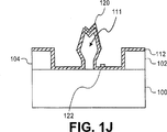
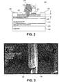
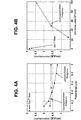
Die
AUSFÜHRLICHE BESCHREIBUNGDETAILED DESCRIPTION
Verschiedene Ausführungsformen eines Halbleiterbauelements und eines Fabrikationsverfahrens zu dessen Erstellung werden unter Bezugnahme auf die Zeichnungen erörtert, in denen gleiche Zahlen sich auf gleiche Komponenten beziehen und in denen eine einzelne Bezugszahl verwendet werden kann, um eine bestimmte exemplarische Ausführung unter mehreren gleichen Komponenten zu bezeichnen.Various embodiments of a semiconductor device and fabrication method of making the same will be discussed with reference to the drawings in which like numerals refer to like components and in which a single numeral may be used to designate a particular exemplary embodiment among a plurality of like components.
Unter Bezugnahme auf die
Unter Bezugnahme auf
Unter Bezugnahme auf
Die Lackschicht
Unter Bezugnahme auf
Unter Bezugnahme auf
Vor der Metallfilmabscheidung kann eine Nass- oder Trockenvertiefungsätzung in die Barrierenschicht durchgeführt werden, wobei entweder Nass- oder Trockenätztechniken verwendet werden, wie etwa beispielsweise reaktives Ionenätzen (RIE) oder induktiv gekoppeltes Plasmaätzen (ICP).Prior to metal film deposition, a wet or dry well etch may be performed in the barrier layer using either wet or dry etch techniques, such as, for example, reactive ion etching (RIE) or inductively coupled plasma etching (ICP).
Unter Bezugnahme auf
Unter Bezugnahme auf
Unter Bezugnahme auf
Unter Bezugnahme auf
Unter Bezugnahme auf
Die Dicke der feldabschwächenden Platten ist auf Werte kleiner als die T-Gate-Stielhöhe begrenzt, um einen vollständigen und durchgängigen Feldplattenbruch entlang ihrer Länge sicherzustellen. Die seitlichen Abmessungen der Feldplatte werden durch das Bauelementlayout und die Feldplattenexpositionsdosis gesteuert. Weiterhin kann die Länge des in der Lackschicht
Dadurch kann das neuartige, in
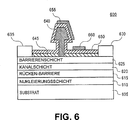
Unter Bezugnahme auf
Das Halbleiterbauelement
Eine erste Feldplatte
Unter Bezugnahme auf
Unter Bezugnahme auf
Unter Bezugnahme auf
Eine bevorzugt aus SiN bestehende zweite Dielektrikumsschicht
Die erste Dielektrikumsschicht
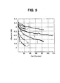
Die oben erörterten Vorrichtungen und Verfahren und ihre erfindungsgemäßen Prinzipien sollen und werden ein Halbleiterbauelement mit einer feldabschwächenden Platte zum Minimieren elektrischer Felder mit einem Minimum an Leistungsverstärkungsverlust herstellen, wodurch die Bauelementdurchschlagsspannung heraufgesetzt, das Fangen von Ladungen auf ein Minimum reduziert und der Gateleckstrom reduziert wird. Es kann eine feldabschwächende Platte von 0,1 Mikrometern erreicht werden, wobei diese dennoch den Vorzug eines reduzierten elektrischen Feldes bereitstellt.The devices and methods discussed above, and their principles of the invention, are and are intended to provide a semiconductor device with a field attenuating plate for minimizing electric fields with a minimum of power gain loss, thereby increasing device breakdown voltage, minimizing charge trapping, and reducing gate leakage current. A field-attenuating plate of 0.1 microns can be achieved while still providing the benefit of a reduced electric field.
Es wird erwartet, dass der Durchschnittsfachmann angesichts der oben beschriebenen Prinzipien, Konzepte und Beispiele in der Lage sein wird, andere alternative Prozeduren und Konstruktionen zu implementieren, die die gleichen Vorzüge bieten. Beispielsweise könnte die feldabschwächende Platte vor der Ausbildung des T-Gates ausgebildet werden. Das T-Gate kann danach unter Verwendung einer Reihe von isotropen Trockenätzungen ausgebildet werden.It is expected that those of ordinary skill in the art, given the principles, concepts and examples described above, will be able to implement other alternative procedures and designs that offer the same benefits. For example, the field attenuating plate could be formed prior to the formation of the T-gate. The T-gate may then be formed using a series of dry isotropic etches.
Claims (15)
Applications Claiming Priority (2)
| Application Number | Priority Date | Filing Date | Title |
|---|---|---|---|
| US11/976,590 | 2007-10-25 | ||
| US11/976,590 US7800132B2 (en) | 2007-10-25 | 2007-10-25 | High electron mobility transistor semiconductor device having field mitigating plate and fabrication method thereof |
Publications (2)
| Publication Number | Publication Date |
|---|---|
| DE102008052595A1 DE102008052595A1 (en) | 2009-04-30 |
| DE102008052595B4 true DE102008052595B4 (en) | 2011-05-12 |
Family
ID=40490497
Family Applications (1)
| Application Number | Title | Priority Date | Filing Date |
|---|---|---|---|
| DE102008052595A Active DE102008052595B4 (en) | 2007-10-25 | 2008-10-21 | A method of fabricating a semiconductor device as a high electron mobility semiconductor device (HEMT) having a field weakening plate and semiconductor device |
Country Status (3)
| Country | Link |
|---|---|
| US (1) | US7800132B2 (en) |
| JP (1) | JP2009105405A (en) |
| DE (1) | DE102008052595B4 (en) |
Cited By (1)
| Publication number | Priority date | Publication date | Assignee | Title |
|---|---|---|---|---|
| DE102016123934A1 (en) * | 2016-12-09 | 2018-06-14 | United Monolithic Semiconductors Gmbh | Method for producing a transistor |
Families Citing this family (25)
| Publication number | Priority date | Publication date | Assignee | Title |
|---|---|---|---|---|
| US8431962B2 (en) * | 2007-12-07 | 2013-04-30 | Northrop Grumman Systems Corporation | Composite passivation process for nitride FET |
| US8754496B2 (en) * | 2009-04-14 | 2014-06-17 | Triquint Semiconductor, Inc. | Field effect transistor having a plurality of field plates |
| KR101632314B1 (en) | 2009-09-11 | 2016-06-22 | 삼성전자주식회사 | Field Effect Semiconductor Device and Manufacturing Method of the Same |
| US8541817B2 (en) * | 2009-11-06 | 2013-09-24 | Nitek, Inc. | Multilayer barrier III-nitride transistor for high voltage electronics |
| JP5660280B2 (en) * | 2010-03-27 | 2015-01-28 | 日本電気株式会社 | Field effect transistor, method of manufacturing field effect transistor, and electronic device |
| DE102010016993A1 (en) | 2010-05-18 | 2011-11-24 | United Monolithic Semiconductors Gmbh | Semiconductor device |
| US8710511B2 (en) | 2011-07-29 | 2014-04-29 | Northrop Grumman Systems Corporation | AIN buffer N-polar GaN HEMT profile |
| US8455312B2 (en) * | 2011-09-12 | 2013-06-04 | Cindy X. Qiu | Fabrication methods for T-gate and inverted L-gate structure for high frequency devices and circuits |
| US8530978B1 (en) * | 2011-12-06 | 2013-09-10 | Hrl Laboratories, Llc | High current high voltage GaN field effect transistors and method of fabricating same |
| WO2014050054A1 (en) * | 2012-09-28 | 2014-04-03 | パナソニック株式会社 | Semiconductor device |
| KR102065114B1 (en) * | 2013-03-14 | 2020-01-10 | 삼성전자주식회사 | Operating method of reducing current collapse of power device |
| US9048184B2 (en) * | 2013-03-15 | 2015-06-02 | Northrop Grumman Systems Corporation | Method of forming a gate contact |
| JP2015195288A (en) * | 2014-03-31 | 2015-11-05 | 住友電工デバイス・イノベーション株式会社 | Semiconductor device and semiconductor device manufacturing method |
| US10276712B2 (en) | 2014-05-29 | 2019-04-30 | Hrl Laboratories, Llc | III-nitride field-effect transistor with dual gates |
| JP6436531B2 (en) * | 2015-01-30 | 2018-12-12 | 住友電工デバイス・イノベーション株式会社 | Manufacturing method of semiconductor device |
| CN106328703B (en) * | 2015-06-18 | 2019-07-19 | 台达电子工业股份有限公司 | Semiconductor device |
| TWI626742B (en) | 2015-06-18 | 2018-06-11 | 台達電子工業股份有限公司 | Semiconductor device |
| US9812532B1 (en) | 2015-08-28 | 2017-11-07 | Hrl Laboratories, Llc | III-nitride P-channel transistor |
| EP3378097A4 (en) | 2015-11-19 | 2019-09-11 | HRL Laboratories, LLC | Iii-nitride field-effect transistor with dual gates |
| JP6811737B2 (en) * | 2018-03-13 | 2021-01-13 | 株式会社東芝 | Semiconductor device |
| JP2020150193A (en) * | 2019-03-15 | 2020-09-17 | 株式会社東芝 | Semiconductor device |
| US11075271B2 (en) * | 2019-10-14 | 2021-07-27 | Cree, Inc. | Stepped field plates with proximity to conduction channel and related fabrication methods |
| WO2021230283A1 (en) * | 2020-05-13 | 2021-11-18 | ヌヴォトンテクノロジージャパン株式会社 | Semiconductor device for power amplification |
| WO2023175820A1 (en) * | 2022-03-17 | 2023-09-21 | 三菱電機株式会社 | Method for producing semiconductor device |
| WO2023205936A1 (en) * | 2022-04-24 | 2023-11-02 | 华为技术有限公司 | Semiconductor device and preparation method therefor |
Citations (2)
| Publication number | Priority date | Publication date | Assignee | Title |
|---|---|---|---|---|
| US20070295993A1 (en) * | 2005-11-29 | 2007-12-27 | The Hong Kong University Of Science And Technology | Low Density Drain HEMTs |
| US20080124851A1 (en) * | 2005-04-07 | 2008-05-29 | An-Ping Zhang | GaN-based high electron mobility transistor and method for making the same |
Family Cites Families (26)
| Publication number | Priority date | Publication date | Assignee | Title |
|---|---|---|---|---|
| US6548333B2 (en) * | 2000-12-01 | 2003-04-15 | Cree, Inc. | Aluminum gallium nitride/gallium nitride high electron mobility transistors having a gate contact on a gallium nitride based cap segment |
| US7622322B2 (en) * | 2001-03-23 | 2009-11-24 | Cornell Research Foundation, Inc. | Method of forming an AlN coated heterojunction field effect transistor |
| US7030428B2 (en) * | 2001-12-03 | 2006-04-18 | Cree, Inc. | Strain balanced nitride heterojunction transistors |
| TW200305283A (en) * | 2001-12-06 | 2003-10-16 | Hrl Lab Llc | High power-low noise microwave GaN heterojunction field effet transistor |
| US6852615B2 (en) * | 2002-06-10 | 2005-02-08 | Hrl Laboratories, Llc | Ohmic contacts for high electron mobility transistors and a method of making the same |
| US6982204B2 (en) * | 2002-07-16 | 2006-01-03 | Cree, Inc. | Nitride-based transistors and methods of fabrication thereof using non-etched contact recesses |
| US7112860B2 (en) * | 2003-03-03 | 2006-09-26 | Cree, Inc. | Integrated nitride-based acoustic wave devices and methods of fabricating integrated nitride-based acoustic wave devices |
| JP3940699B2 (en) * | 2003-05-16 | 2007-07-04 | 株式会社東芝 | Power semiconductor device |
| US7098490B2 (en) * | 2003-06-02 | 2006-08-29 | Hrl Laboratories, Llc | GaN DHFET |
| US7501669B2 (en) * | 2003-09-09 | 2009-03-10 | Cree, Inc. | Wide bandgap transistor devices with field plates |
| US7126426B2 (en) * | 2003-09-09 | 2006-10-24 | Cree, Inc. | Cascode amplifier structures including wide bandgap field effect transistor with field plates |
| JP4339657B2 (en) * | 2003-09-30 | 2009-10-07 | 富士通株式会社 | Semiconductor device and manufacturing method thereof |
| US20070138506A1 (en) * | 2003-11-17 | 2007-06-21 | Braddock Walter D | Nitride metal oxide semiconductor integrated transistor devices |
| US7045404B2 (en) * | 2004-01-16 | 2006-05-16 | Cree, Inc. | Nitride-based transistors with a protective layer and a low-damage recess and methods of fabrication thereof |
| US7612390B2 (en) | 2004-02-05 | 2009-11-03 | Cree, Inc. | Heterojunction transistors including energy barriers |
| US7573078B2 (en) * | 2004-05-11 | 2009-08-11 | Cree, Inc. | Wide bandgap transistors with multiple field plates |
| US7229903B2 (en) * | 2004-08-25 | 2007-06-12 | Freescale Semiconductor, Inc. | Recessed semiconductor device |
| US7161194B2 (en) * | 2004-12-06 | 2007-01-09 | Cree, Inc. | High power density and/or linearity transistors |
| JP2006269862A (en) * | 2005-03-25 | 2006-10-05 | Oki Electric Ind Co Ltd | Wafer for forming semiconductor device, its manufacturing method, and field effect transistor |
| US7863648B2 (en) * | 2005-06-10 | 2011-01-04 | Nec Corporation | Field effect transistor |
| US7855401B2 (en) * | 2005-06-29 | 2010-12-21 | Cree, Inc. | Passivation of wide band-gap based semiconductor devices with hydrogen-free sputtered nitrides |
| US7548112B2 (en) * | 2005-07-21 | 2009-06-16 | Cree, Inc. | Switch mode power amplifier using MIS-HEMT with field plate extension |
| JP5162823B2 (en) * | 2005-12-08 | 2013-03-13 | 三菱電機株式会社 | Semiconductor device and manufacturing method of semiconductor device |
| US7592211B2 (en) * | 2006-01-17 | 2009-09-22 | Cree, Inc. | Methods of fabricating transistors including supported gate electrodes |
| US7709269B2 (en) * | 2006-01-17 | 2010-05-04 | Cree, Inc. | Methods of fabricating transistors including dielectrically-supported gate electrodes |
| JP2007250910A (en) * | 2006-03-16 | 2007-09-27 | Matsushita Electric Ind Co Ltd | Semiconductor device |
-
2007
- 2007-10-25 US US11/976,590 patent/US7800132B2/en active Active
-
2008
- 2008-10-21 DE DE102008052595A patent/DE102008052595B4/en active Active
- 2008-10-21 JP JP2008271153A patent/JP2009105405A/en active Pending
Patent Citations (2)
| Publication number | Priority date | Publication date | Assignee | Title |
|---|---|---|---|---|
| US20080124851A1 (en) * | 2005-04-07 | 2008-05-29 | An-Ping Zhang | GaN-based high electron mobility transistor and method for making the same |
| US20070295993A1 (en) * | 2005-11-29 | 2007-12-27 | The Hong Kong University Of Science And Technology | Low Density Drain HEMTs |
Cited By (1)
| Publication number | Priority date | Publication date | Assignee | Title |
|---|---|---|---|---|
| DE102016123934A1 (en) * | 2016-12-09 | 2018-06-14 | United Monolithic Semiconductors Gmbh | Method for producing a transistor |
Also Published As
| Publication number | Publication date |
|---|---|
| US7800132B2 (en) | 2010-09-21 |
| DE102008052595A1 (en) | 2009-04-30 |
| JP2009105405A (en) | 2009-05-14 |
| US20090108299A1 (en) | 2009-04-30 |
Similar Documents
| Publication | Publication Date | Title |
|---|---|---|
| DE102008052595B4 (en) | A method of fabricating a semiconductor device as a high electron mobility semiconductor device (HEMT) having a field weakening plate and semiconductor device | |
| DE112005001179B4 (en) | Improved dielectric passivation for semiconductor devices and processes | |
| DE112010003087B4 (en) | Method of forming transistor devices from Group III nitride | |
| DE102016100060B4 (en) | TRANSISTOR WITH HIGH ELECTRON MOBILITY AND METHOD FOR ITS MANUFACTURING | |
| EP2135286B1 (en) | Semiconductor component with field plate structure and method for producing the same | |
| DE102008060704B4 (en) | Field effect transistor device and method for its production with a composite passivation process | |
| DE102013105713B4 (en) | Method of manufacturing a semiconductor device | |
| DE102010060138B4 (en) | Lateral HEMT | |
| DE69835204T2 (en) | DESIGN AND MANUFACTURE OF ELECTRONIC ARRANGEMENTS WITH InAlAsSb / AlSb BARRIER | |
| DE102013102248A1 (en) | Semiconductor device and method for manufacturing a semiconductor device | |
| DE19846063A1 (en) | Method of manufacturing a double-gate MOSFET | |
| DE112004001442T5 (en) | Vary the carrier mobility in semi-conductor devices to achieve overall design goals | |
| DE112014003545T5 (en) | Integrated threshold matched threshold voltage circuit and method of making same | |
| EP1354342B1 (en) | Method for producing a semiconductor component comprising a t-shaped contact electrode | |
| DE102017127182A1 (en) | Gate structure and method for its production | |
| EP0823728B1 (en) | Method of manufacturing a field effect transistor | |
| WO1993013560A1 (en) | Electronic component and process for making it | |
| DE3706274A1 (en) | Semiconductor component and method of fabricating it | |
| EP1380047B1 (en) | Method for producing a semiconductor component comprising a t-shaped contact electrode | |
| DE102017125803B4 (en) | A semiconductor device having an enhancement type transistor structure | |
| WO2018091699A1 (en) | Gate structure and method for producing same | |
| EP3552241A1 (en) | Method for producing a transistor | |
| DE4142595C2 (en) | Electronic component and manufacturing method | |
| DE102022209807A1 (en) | Lateral gallium nitride transistor with stepped edge area | |
| DE4142654A1 (en) | P-channel or N-channel permeable base transistor - has screen-type laterally structured layer for controlling space charge zone |
Legal Events
| Date | Code | Title | Description |
|---|---|---|---|
| OM8 | Search report available as to paragraph 43 lit. 1 sentence 1 patent law | ||
| 8110 | Request for examination paragraph 44 | ||
| R020 | Patent grant now final |
Effective date: 20110813 |
|
| R081 | Change of applicant/patentee |
Owner name: NORTHROP GRUMMAN SYSTEMS CORPORATION (N.D.GES., US Free format text: FORMER OWNER: NORTHROP GRUMMAN SPACE & MISSION SYSTEMS CORPORATION, LOS ANGELES, CALIF., US Effective date: 20120809 Owner name: NORTHROP GRUMMAN SYSTEMS CORPORATION (N.D.GES., US Free format text: FORMER OWNER: NORTHROP GRUMMAN SPACE & MISSION SYSTEMS CORPORATION, LOS ANGELES, US Effective date: 20120809 Owner name: NORTHROP GRUMMAN SYSTEMS CORP. (N.D.GES.D. STA, US Free format text: FORMER OWNER: NORTHROP GRUMMAN SPACE & MISSION SYSTEMS CORPORATION, LOS ANGELES, US Effective date: 20120809 |
|
| R082 | Change of representative |
Representative=s name: DAUB, THOMAS, DIPL.-ING., DE Effective date: 20120809 Representative=s name: THOMAS DAUB, DE Effective date: 20120809 |
|
| R082 | Change of representative |
Representative=s name: DAUB, THOMAS, DIPL.-ING., DE |
|
| R081 | Change of applicant/patentee |
Owner name: NORTHROP GRUMMAN SYSTEMS CORPORATION (N.D.GES., US Free format text: FORMER OWNER: NORTHROP GRUMMAN SYSTEMS CORP. (N.D.GES.D. STAATES DELAWARE), LOS ANGELES, CALIF., US Effective date: 20121210 Owner name: NORTHROP GRUMMAN SYSTEMS CORPORATION (N.D.GES., US Free format text: FORMER OWNER: NORTHROP GRUMMAN SYSTEMS CORP. (N.D.GES.D. STAATES DELAWARE), LOS ANGELES, US Effective date: 20121210 |
|
| R082 | Change of representative |
Representative=s name: DAUB, THOMAS, DIPL.-ING., DE Effective date: 20121210 |