CN213661598U - Radio frequency L-PA Mid device, radio frequency transceiving system and communication equipment - Google Patents
Radio frequency L-PA Mid device, radio frequency transceiving system and communication equipment Download PDFInfo
- Publication number
- CN213661598U CN213661598U CN202022859774.3U CN202022859774U CN213661598U CN 213661598 U CN213661598 U CN 213661598U CN 202022859774 U CN202022859774 U CN 202022859774U CN 213661598 U CN213661598 U CN 213661598U
- Authority
- CN
- China
- Prior art keywords
- frequency
- radio frequency
- circuit
- port
- low
- Prior art date
- Legal status (The legal status is an assumption and is not a legal conclusion. Google has not performed a legal analysis and makes no representation as to the accuracy of the status listed.)
- Active
Links
- 238000004891 communication Methods 0.000 title claims abstract description 29
- 238000001914 filtration Methods 0.000 claims description 61
- 230000005540 biological transmission Effects 0.000 claims description 57
- 238000012545 processing Methods 0.000 claims description 24
- 230000008878 coupling Effects 0.000 claims description 21
- 238000010168 coupling process Methods 0.000 claims description 21
- 238000005859 coupling reaction Methods 0.000 claims description 21
- 230000003321 amplification Effects 0.000 claims description 6
- 238000003199 nucleic acid amplification method Methods 0.000 claims description 6
- 238000003780 insertion Methods 0.000 abstract description 25
- 230000037431 insertion Effects 0.000 abstract description 25
- 238000010586 diagram Methods 0.000 description 16
- 230000035945 sensitivity Effects 0.000 description 16
- 238000000034 method Methods 0.000 description 9
- 230000008569 process Effects 0.000 description 8
- 102100032533 ADP/ATP translocase 1 Human genes 0.000 description 5
- 101000768061 Escherichia phage P1 Antirepressor protein 1 Proteins 0.000 description 5
- 101000796932 Homo sapiens ADP/ATP translocase 1 Proteins 0.000 description 5
- 238000005516 engineering process Methods 0.000 description 5
- 102220491086 ADP-ribosylation factor 6_N28A_mutation Human genes 0.000 description 4
- 102100026396 ADP/ATP translocase 2 Human genes 0.000 description 4
- 101000718417 Homo sapiens ADP/ATP translocase 2 Proteins 0.000 description 4
- 101001045846 Homo sapiens Histone-lysine N-methyltransferase 2A Proteins 0.000 description 4
- 102100036407 Thioredoxin Human genes 0.000 description 4
- 101150093547 AUX1 gene Proteins 0.000 description 3
- 101100125299 Agrobacterium rhizogenes aux2 gene Proteins 0.000 description 3
- 101100208110 Arabidopsis thaliana TRX4 gene Proteins 0.000 description 3
- 101100425275 Dictyostelium discoideum trxC gene Proteins 0.000 description 3
- 101100425276 Dictyostelium discoideum trxD gene Proteins 0.000 description 3
- 102100022102 Histone-lysine N-methyltransferase 2B Human genes 0.000 description 3
- 101001045848 Homo sapiens Histone-lysine N-methyltransferase 2B Proteins 0.000 description 3
- 101100154863 Mus musculus Txndc2 gene Proteins 0.000 description 3
- 101100367246 Saccharomyces cerevisiae (strain ATCC 204508 / S288c) SWA2 gene Proteins 0.000 description 3
- 101100101240 Schizosaccharomyces pombe (strain 972 / ATCC 24843) txl1 gene Proteins 0.000 description 3
- 101150096347 TRX3 gene Proteins 0.000 description 3
- 238000011161 development Methods 0.000 description 3
- 238000010295 mobile communication Methods 0.000 description 3
- 101150041689 SLC25A5 gene Proteins 0.000 description 2
- 101150092978 Slc25a4 gene Proteins 0.000 description 2
- 241001125929 Trisopterus luscus Species 0.000 description 2
- 238000001514 detection method Methods 0.000 description 2
- 238000012986 modification Methods 0.000 description 2
- 230000004048 modification Effects 0.000 description 2
- 238000012360 testing method Methods 0.000 description 2
- 102100026397 ADP/ATP translocase 3 Human genes 0.000 description 1
- 101000718437 Homo sapiens ADP/ATP translocase 3 Proteins 0.000 description 1
- 235000008331 Pinus X rigitaeda Nutrition 0.000 description 1
- 235000011613 Pinus brutia Nutrition 0.000 description 1
- 241000018646 Pinus brutia Species 0.000 description 1
- 101100532456 Rattus norvegicus Slc28a2 gene Proteins 0.000 description 1
- 101710168651 Thioredoxin 1 Proteins 0.000 description 1
- 230000006872 improvement Effects 0.000 description 1
- 238000002955 isolation Methods 0.000 description 1
- 230000005404 monopole Effects 0.000 description 1
- 230000005855 radiation Effects 0.000 description 1
- 238000012827 research and development Methods 0.000 description 1
- 239000000523 sample Substances 0.000 description 1
Images


Classifications
-
- H—ELECTRICITY
- H04—ELECTRIC COMMUNICATION TECHNIQUE
- H04B—TRANSMISSION
- H04B1/00—Details of transmission systems, not covered by a single one of groups H04B3/00 - H04B13/00; Details of transmission systems not characterised by the medium used for transmission
- H04B1/005—Details of transmission systems, not covered by a single one of groups H04B3/00 - H04B13/00; Details of transmission systems not characterised by the medium used for transmission adapting radio receivers, transmitters andtransceivers for operation on two or more bands, i.e. frequency ranges
- H04B1/0053—Details of transmission systems, not covered by a single one of groups H04B3/00 - H04B13/00; Details of transmission systems not characterised by the medium used for transmission adapting radio receivers, transmitters andtransceivers for operation on two or more bands, i.e. frequency ranges with common antenna for more than one band
- H04B1/006—Details of transmission systems, not covered by a single one of groups H04B3/00 - H04B13/00; Details of transmission systems not characterised by the medium used for transmission adapting radio receivers, transmitters andtransceivers for operation on two or more bands, i.e. frequency ranges with common antenna for more than one band using switches for selecting the desired band
-
- H—ELECTRICITY
- H04—ELECTRIC COMMUNICATION TECHNIQUE
- H04B—TRANSMISSION
- H04B1/00—Details of transmission systems, not covered by a single one of groups H04B3/00 - H04B13/00; Details of transmission systems not characterised by the medium used for transmission
- H04B1/38—Transceivers, i.e. devices in which transmitter and receiver form a structural unit and in which at least one part is used for functions of transmitting and receiving
- H04B1/40—Circuits
- H04B1/401—Circuits for selecting or indicating operating mode
Abstract
The application provides a radio frequency L-PA Mid device, a radio frequency transceiving system and a communication device, wherein, the radio frequency L-PA Mid device is configured with a transmitting port, an antenna port and a plurality of receiving ports, wherein, the radio frequency L-PA Mid device comprises: the first transmitting circuit is used for amplifying the received preset low-frequency signal; the second transmitting circuit is used for amplifying the received low-frequency band signals; the receiving circuit is connected with the plurality of receiving ports and is used for amplifying the received preset low-frequency signals and the plurality of low-frequency band signals; and a plurality of first ends of the switch circuit are respectively connected with the first transmitting circuit, the second transmitting circuit and the receiving circuit, and a second end of the switch circuit is connected with the antenna port and used for selectively conducting radio frequency paths between the first transmitting circuit, the second transmitting circuit and the receiving circuit and the antenna port, so that link insertion loss can be reduced, and the communication performance of the radio frequency L-PA Mid device can be improved.
Description
Technical Field
The present application relates to the field of radio frequency technologies, and in particular, to a radio frequency L-PA Mid device, a radio frequency transceiving system, and a communication device.
Background
With the development and progress of the technology, the 5G mobile communication technology is gradually beginning to be applied to electronic devices. The 5G mobile communication technology communication frequency is higher than that of the 4G mobile communication technology. In a conventional rf transceiving system, an rf front-end module for supporting a predetermined low-frequency signal (e.g., an N28 band signal) is provided, and a transceiver device with a built-in power amplifier and an external circuit disposed at the periphery of the transceiver device are provided in the module to support transceiving processing of an N28 band signal.
However, the link loss of the transceiving link for the preset low frequency signal in the conventional rf front-end module is too large, which results in poor performance of the rf front-end module.
SUMMERY OF THE UTILITY MODEL
The embodiment of the application provides a radio frequency L-PA Mid device, a radio frequency transceiving system and communication equipment, which can reduce link insertion loss to improve the communication performance of the radio frequency L-PA Mid device.
A radio frequency L-PA Mid device configured with a transmit port, an antenna port, and a plurality of receive ports for connection to a radio frequency transceiver, wherein the radio frequency L-PA Mid device comprises:
the first transmitting circuit is connected with the transmitting port and used for amplifying the received preset low-frequency signal;
the second transmitting circuit is connected with the transmitting port and used for amplifying the received low-frequency band signals;
the receiving circuit is connected with the plurality of receiving ports and is used for amplifying the received preset low-frequency signals and the plurality of low-frequency-band signals;
and a plurality of first ends of the switch circuit are respectively connected with the first transmitting circuit, the second transmitting circuit and the receiving circuit, and a second end of the switch circuit is connected with the antenna port and used for selectively conducting the radio frequency paths among the first transmitting circuit, the second transmitting circuit and the receiving circuit and the antenna port.
A radio frequency transceiving system comprising:
a radio frequency L-PA Mid device as described previously;
the antenna group comprises a first antenna, and the first antenna is connected with an antenna port of the radio frequency L-PA Mid device;
and the radio frequency transceiver is respectively connected with the transmitting port and the receiving port of the radio frequency L-PA Mid device.
A communication device comprises the radio frequency transceiving system.
The radio frequency L-PA Mid device, the radio frequency transceiving system and the communication equipment comprise the transmitting circuit, the receiving circuit and the switch circuit, namely the first transmitting circuit and the receiving circuit for the preset low-frequency signal (for example, an N28 frequency band signal) are integrated in the radio frequency L-PA Mid device, and compared with the traditional device in which an external duplexer is adopted to support transceiving processing of the preset low-frequency signal, insertion loss of a transceiving link can be reduced, the output power of the device for the preset low-frequency signal is improved, the sensitivity performance of the preset low-frequency signal is improved, and further the communication performance of the device can be improved. Meanwhile, compared with the traditional device, the integrated level of the device can be improved, the area can be saved, and the miniaturization of the device is facilitated. In addition, the logic control of the switch circuit, the laying of a power supply network and the like are all provided by the radio frequency L-PA Mid device, so that other elements of the radio frequency PA Mid radio frequency device cannot be influenced, and meanwhile, the cost can be reduced.
Drawings
In order to more clearly illustrate the embodiments of the present application or the technical solutions in the prior art, the drawings used in the description of the embodiments or the prior art will be briefly described below, it is obvious that the drawings in the following description are only some embodiments of the present application, and for those skilled in the art, other drawings can be obtained according to the drawings without creative efforts.
FIG. 1 is one of the block diagrams of the structure of an RF L-PA Mid device in one embodiment;
FIG. 2 is a second block diagram of the RF L-PA Mid device in one embodiment;
FIG. 3 is a third block diagram of the RF L-PA Mid device in one embodiment;
FIG. 4 is a block diagram of the structure of an RF L-PA Mid device in one embodiment;
FIG. 5 is a block diagram of the structure of an RF L-PA Mid device in one embodiment;
FIG. 6 is a graph of input power versus output power for a power amplifier in one embodiment;
FIG. 7 is a sixth block diagram illustrating the structure of an exemplary RF L-PA Mid device;
FIG. 8 is a seventh block diagram illustrating the structure of an exemplary RF L-PA Mid device;
FIG. 9 is an eighth schematic block diagram of an exemplary RF L-PA Mid device;
FIG. 10 is a block diagram of an exemplary RF transceiver system;
FIG. 11 is a second block diagram illustrating the structure of an RF transceiver system according to an embodiment;
FIG. 12 is a third block diagram illustrating an exemplary RF transceiver system;
FIG. 13 is a block diagram of an exemplary RF transceiver system;
FIG. 14 is a block diagram of an exemplary RF transceiver system;
FIG. 15 is a sixth block diagram illustrating an exemplary RF transceiver system;
FIG. 16 is a seventh block diagram illustrating an exemplary RF transceiver system;
fig. 17 is an eighth block diagram illustrating an exemplary rf transceiver system.
Detailed Description
In order to make the aforementioned objects, features and advantages of the present application more comprehensible, embodiments accompanying the present application are described in detail below with reference to the accompanying drawings. In the following description, numerous specific details are set forth to provide a thorough understanding of the present application, and in the accompanying drawings, preferred embodiments of the present application are set forth. This application may, however, be embodied in many different forms and should not be construed as limited to the embodiments set forth herein. Rather, these embodiments are provided so that this disclosure will be thorough and complete. This application is capable of embodiments in many different forms than those described herein and those skilled in the art will be able to make similar modifications without departing from the spirit of the application and it is therefore not intended to be limited to the specific embodiments disclosed below.
Furthermore, the terms "first", "second" and "first" are used for descriptive purposes only and are not to be construed as indicating or implying relative importance or implicitly indicating the number of technical features indicated. Thus, a feature defined as "first" or "second" may explicitly or implicitly include at least one such feature. In the description of the present application, "plurality" means at least two, e.g., two, three, etc., unless specifically limited otherwise. In the description of the present application, "a number" means at least one, such as one, two, etc., unless specifically limited otherwise.
The radio frequency L-PA Mid device according to the embodiment of the present application may be applied to a communication device having a wireless communication function, where the communication device may be a handheld device, a vehicle-mounted device, a wearable device, a computing device or other processing device connected to a wireless modem, and various forms of User Equipment (UE) (e.g., a Mobile phone), a Mobile Station (MS), and the like. For convenience of description, the above-mentioned devices are collectively referred to as a communication device. The network devices may include base stations, access points, and the like.
The embodiment of the application provides a radio frequency L-PA Mid device. The rf L-PA Mid device can be understood as a Power Amplifier module (Power Amplifier Modules including LNAs) With a built-in low noise Amplifier. The radio frequency L-PA Mid device can support the receiving and transmitting of low-frequency signals of a plurality of different frequency bands and preset low-frequency signals. Therefore, the radio frequency L-PA Mid device in the embodiment of the present application may also be referred to as a Low frequency power amplifier module (Low Band PA Mid With LNA, LB L-PA Mid) With a built-in Low noise amplifier.
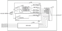
As shown in fig. 1, in one embodiment, the radio frequency L-PA Mid device may be understood as a package structure, and the radio frequency L-PA Mid device is configured with a transmission port 4G LB RFIN, an antenna port LB ANT, and a plurality of reception ports LNA OUT for connecting with a radio frequency transceiver. The transmitting port 4G LB RFIN, the antenna port LB ANT and the plurality of receiving ports LNA OUT configured in the device may be understood as radio frequency pin terminals of the radio frequency L-PA Mid device, and are used for connecting with external devices. Specifically, the receiving port LNA OUT and the low-frequency transmitting port 4G LB RFIN may be used to connect with a radio frequency transceiver; the antenna port LB ANT may be used to connect with an antenna.
Specifically, the radio frequency L-PA Mid device comprises: a first transmitting circuit 110, a second transmitting circuit 120, a receiving circuit 130, and a switching circuit 140. An input terminal of the first transmission circuit 110 is connected to the transmission port 4G LB RFIN, and an output terminal of the first transmission circuit 110 is connected to the switch circuit 140. The first transmitting circuit 110 may amplify the preset low-frequency signal received by the transmitting port 4G LB RFIN. The preset low frequency signal may be a signal of N28 frequency band. An input terminal of the second transmission circuit 120 is connected to the transmission port 4G LB RFIN, and an output terminal of the second transmission circuit 120 is connected to the switch circuit 140. Specifically, the second transmitting circuit 120 may amplify the plurality of point frequency band signals received by the transmitting port 4G LB RFIN. For example, a plurality of radio frequency paths may be provided in the second transmitting circuit 120 to support the transmission of a plurality of low frequency band signals. The frequency bands of the plurality of low frequency band signals at least include B8, B12, B20, B26, N8, B28, N20 and N26 frequency bands. Further, the frequency bands of the plurality of low frequency band signals may also include B13 and B29 frequency bands.
In the embodiment of the present application, it should be noted that, for the radio frequency L-PA Mid device, the relationship between 5G NR and 4G LTE is shown in table 1. As can be seen from table 1, some frequency band ranges of 4G LTE and 5G NR are the same. Therefore, the physical transceiving channels of N26, N8, and N20 share the transceiving channels with B26, B8, and B20, respectively.
TABLE 14G LTE and 5G NR essential information

The receiving circuit 130 is connected to the switch circuit 140 and the plurality of receiving ports LNA OUT, and configured to amplify the received preset low-frequency signal and the plurality of low-frequency signals. That is, the receiving circuit 130 can support the receiving control of the aforementioned preset low frequency signal and any one of the low frequency band signals. The receiving circuit 130 may also be provided with a plurality of rf paths for transmitting a predetermined low frequency signal and each low frequency band signal. For example, respective radio frequency paths may be set for N28, B8, B12, B20, B26, N8, B28, N20, and N26 frequency bands. The antenna port LB ANT, the switch circuit 140, the receiving circuit 130, and any receiving port LNA OUT together form a receiving path, that is, a receiving path may be provided for a preset low-frequency signal and a low-frequency band signal of each frequency band, so as to support receiving processing of the preset low-frequency signal and a plurality of low-frequency band signals.
The switch circuit 140 has a plurality of first terminals of the switch circuit 140 respectively connected to the first transmitting circuit 110, the second transmitting circuit 120, and the receiving circuit 130, and a second terminal of the switch circuit 140 connected to the antenna port LB ANT, for selectively connecting the radio frequency paths between the first transmitting circuit 110, the second transmitting circuit 120, and the receiving circuit 130 and the antenna port LB ANT. That is, the switch circuit 140 may be used to selectively turn on a transmission path or a reception path of a preset low-frequency signal, a plurality of low-frequency band signals.
It should be noted that the switch circuit 140 may include one or more switches, and the number of the first terminals of the switch circuit 140 is related to the number of the radio frequency signals that can be processed by the first transmitting circuit 110, the second transmitting circuit 120, and the receiving circuit 130.
The radio frequency L-PA Mid device includes a first transmitting circuit 110, a second transmitting circuit 120, a receiving circuit 130, and a switch circuit 140, that is, the first transmitting circuit and the receiving circuit 130 for a preset low frequency signal (for example, an N28 frequency band signal) are integrated in the device, and compared with a conventional device in which an external duplexer is used to support the transceiving processing of the preset low frequency signal, the insertion loss of a transceiving link can be reduced, the output power of the device for the preset low frequency signal is improved, the sensitivity performance of the preset low frequency signal is improved, and further, the communication performance of the device can be improved. Meanwhile, compared with the traditional device, the integrated level of the device can be improved, the area can be saved, and the miniaturization of the device is facilitated. In addition, the logic control, the power supply network laying and the like of the switch circuit 140 are provided by the radio frequency L-PA Mid device, so that other elements of the radio frequency PA Mid radio frequency device cannot be influenced, and meanwhile, the cost can be reduced.
As shown in fig. 2, in one embodiment, the switching circuit 140 includes a first switching unit 141 and a second switching unit 142. The first switch unit 141 includes a plurality of first terminals and a second terminal, and the plurality of first terminals of the first switch unit 141 are respectively connected to the second transmitting circuit 120 and the receiving circuit 130. The second switch unit 142 includes two first terminals and a second terminal, the first terminal of the second switch unit 142 is connected to the second terminal of the first switch unit 141, and the second terminal of the second switch unit 142 is connected to the antenna port LB ANT.
Specifically, the first switching unit 141 may be an SPnT switch, and illustratively, the first switching unit 141 may be an SP9T switch, and the second switching unit 142 may be an SPDT switch. In the embodiment of the present application, n may be set according to the number of the plurality of low-band signals and the internal structural features of the second transmitting circuit 120 and the receiving circuit 130, and is not further limited herein.
The transmission path of the preset low-frequency signal in the radio frequency L-PA Mid device is transmission port 4G LB RFIN → first transmission circuit 110 → second switch unit 142 → antenna port LB ANT.
As shown in fig. 3, in one embodiment, the switch circuit 140 includes a multi-channel selection switch 143, wherein a plurality of first terminals of the multi-channel selection switch 143 are respectively connected to the first transmitting circuit 110, the second transmitting circuit 120, and the receiving circuit 130; a second terminal of the multi-channel selection switch 143 is connected to the antenna port LB ANT.
Specifically, the multi-channel selection switch 143 can be a SPmT switch, where m ≧ 4. Illustratively, the multi-channel select switch 143 may be an SP10T switch. In the embodiment of the present application, m may be set according to the preset low frequency signal, the number of the plurality of low frequency band signals, and the internal structural features of the first transmitting circuit 110, the second transmitting circuit 120, and the receiving circuit 130, and is not further limited herein.
The transmission path of the low-frequency signal in the radio frequency L-PA Mid device is preset to be the transmission port 4G LB RFIN → the first transmission circuit 110 → the multi-channel selection switch 143 → the antenna port LB ANT.
Based on the rf L-PA Mid device shown in fig. 2 and 3, the transmission path based on the preset low frequency signal shown in fig. 2 has different switches on the transmission path compared to the transmission path of the preset low frequency signal shown in fig. 3, wherein one is the SPDT switch and the other is the SPmT switch (m ≧ 4), and the insertion loss of the SPDT switch is lower than that of the SPmT switch, so that the insertion loss values of the transmission path and the reception path of the preset low frequency signal (e.g., the N28 band signal) can be reduced, and therefore, the transmission power and sensitivity of the preset low frequency signal can be improved.
Meanwhile, the multi-channel selection switch 143 in the radio frequency L-PA Mid device shown in fig. 3 reduces the usage of the primary switch unit, compared to the first switch unit 141 and the second switch unit 142 in the radio frequency L-PA Mid device shown in fig. 2, and thus can reduce the insertion loss of any transmission path. For the transmission paths of multiple low-frequency band signals, the radio frequency L-PA Mid device shown in fig. 3 can reduce the insertion loss by 0.5dB, and further can increase the output power of multiple low-frequency band signals at the antenna port LB ANT, so as to achieve 26.0dBm required by the development and development standards issued by each large operator.
Referring to fig. 1 to fig. 3, in one embodiment, the number of the transmission ports 4G LB RFIN is plural, and the plural transmission ports are respectively denoted as a first transmission port 4G LB0 RFIN and a second transmission port 4G LB1 RFIN, wherein the input end of the first transmission circuit 110 is connected to the first transmission port 4G LB0 RFIN, and the input end of the second transmission circuit 120 is connected to the second transmission port 4G LB1 RFIN. That is, the input of the first power amplifier is connected to the first transmit port 4G LB0 RFIN, and the input of the second power amplifier is connected to the second transmit port 4G LB1 RFIN.
Referring to fig. 2 and 3, in one embodiment, the first transmitting circuit 110 includes a first power amplifier 111 and a first filtering unit 112. The second transmitting circuit 120 includes a second power amplifier 121, a fourth switching unit 122, and a plurality of second filtering units 123. The input end of the first power amplifier 111 is connected to a second end of the third switching unit for performing power amplification on the received preset low-frequency signal, and the first filtering unit 112 is respectively connected to the output end of the first power amplifier 111 and the switching circuit 140 for filtering the received preset low-frequency signal. Specifically, when the predetermined low band signal is the N28 band signal, the first power amplifier 111 and the first filtering unit 112 thereof can support the related processing of the N28 band signal. It should be noted that, after the filtering process of the first filtering unit 112, it may correspondingly output the N28 frequency band signal without noise. The transmitting port 4G LB RFIN, the third switching unit, the first power amplifier 111, the first filtering unit 112, the switching circuit 140, and the antenna port LB ANT form a first transmitting path, which is used for supporting a transmitting process of a preset low-frequency signal.
The input end of the second power amplifier 121 is connected to another second end of the third switching unit, and is configured to perform power amplification on the received multiple preset low frequency band signals. A first end of the fourth switching unit 122 is connected to the output end of the first power amplifier 111, an input end of each second filtering unit 123 is correspondingly connected to a second end of the fourth switching unit 122, an output end of each second filtering unit 123 is correspondingly connected to the switching circuit 140, and the output ends of the second filtering units 123 are used for filtering the received low-frequency band signals, and the frequency bands of the low-frequency band signals output by each second filtering unit 123 are different. Specifically, the second power amplifier 121 may perform power amplification processing on a plurality of low-frequency band signals received through the transmission port 4G LB RFIN, and further transmit the low-frequency band signals processed by the second power amplifier 121 to each second filtering unit 123 through the fourth switching unit 122; the frequency band of the low frequency band signal output by each second filtering unit 123 is different. It will be appreciated that the filter paths in the plurality of transmit paths are independent of each other and do not coincide with each other.
Specifically, the second filtering unit 123 allows only low-frequency band signals of a preset frequency band to pass through. For example, if the frequency bands of the low-frequency band signals can be eight different frequency bands, i.e., B12(N12), B8(N8), B20(N20), and B26(N26), four second filtering units 123 (i.e., four filters) can be correspondingly disposed to implement the filtering process for the eight low-frequency band signals. Accordingly, the fourth switching unit 122 may be an SP4T switch, wherein a first terminal of the SP4T switch is connected to the output terminal of the second power amplifier 121, and four second terminals of the SP4T switch are connected to the four second filtering units 123 in a one-to-one correspondence. After the filtering processing performed by the eight second filtering units 123, the eight low-frequency band signals B12(N12), B8(N8), B20(N20), and B26(N26) can be correspondingly output to the switch circuit 140.
The transmitting port 4G LB RFIN, the fourth switching unit 122, and the second filtering unit 123 may form a radio frequency path, where a frequency band of the low-frequency band signal output by the second filtering unit 123 corresponds to the radio frequency path of the frequency band. For example, the rf path in which the second filtering unit 123 outputting the B8/N8 band is located may be understood as a B8/N8 rf path, and the rf path in which the second filtering unit 123 outputting the B20/N20 band is located may be understood as a B20/N20 rf path. Further, the transmitting port 4G LB RFIN, the second power amplifier 121, the fourth switching unit 122, the second filtering unit 123, the switching circuit 140, and the antenna port LB ANT form a second transmitting path, where the second transmitting path is used to transmit radio frequency signals of any low frequency band.
As shown in fig. 4 and 5, in one embodiment, the radio frequency L-PA Mid device is configured with one transmit port 4G LB RFIN. The radio frequency L-PA Mid device further includes a third switching unit 150, a first end of the third switching unit 150 is connected to the transmit port 4G LB RFIN, and two second ends of the third switching unit 150 are respectively connected to the input end of the first transmit circuit 110 and the input end of the second transmit circuit 120. Specifically, the third switching unit 150 may be an SPDT switch, a single terminal of the SPDT switch is connected to the transmission port 4G LB RFIN, and two selection terminals of the SPDT switch are respectively connected to the input terminal of the first power amplifier 111 and the input terminal of the second power amplifier 121.
In this embodiment, by arranging the third switch unit 150 between the transmission port 4G LB RFIN and the first power amplifier 111 (i.e., the front end of the power amplifier), the number of the transmission ports 4G LB RFIN can be reduced from 2 to 1, so as to save the number of the transmission ports 4G LB RFIN of the radio frequency L-PA Mid device, and further reduce the resources of the radio frequency input interface of the radio frequency transceiver connected to the transmission ports 4G LB RFIN. Meanwhile, based on the formula Pout ═ Pin + Gain, where Pout is the output power, Pin is the input power, and Gain is the Gain of the device. From this equation, the output power of the power amplifier is related to the input power and the device gain. As shown in fig. 6, the maximum linear output power of the power amplifier is PoutE, and the corresponding input power is PinE. Since the SPDT switch is at the input end of the first power amplifier 111, it will increase the insertion loss of the rf input end, and referring to the insertion loss data of the SPDT switch in table 2, the insertion loss in the LB frequency band is 0.2dB, while the output power of the rf transceiver needs to be increased by 0.2dB, which has no influence on the rf input signal quality.
TABLE 2 SPDT switch insertion loss table
| Frequency (MHz) | 1000~1600 | 1600~3000 | 3000~4500 |
| Loss (dB) | 0.20 | 0.25 | 0.30 |
Therefore, the maximum linear output power cannot be influenced by adding the SPDT switch, namely the transmission output power and the performance thereof cannot be influenced.
As shown in fig. 7, 8 and 9, in one embodiment, the receiving circuit 130 includes a first low noise amplifier 131, a third filtering unit 132, at least one second low noise amplifier 133, a fifth switching unit 134 and a plurality of fourth filtering units 135. The output end of the first low noise amplifier 131 is connected to a receiving port LNA OUT, and is configured to amplify a received preset low frequency signal; the third filtering unit 132 is respectively connected to the input terminal of the first low noise amplifier 131 and the switching circuit 140, and is configured to filter the received preset low frequency signal. Specifically, when the predetermined low band signal is the N28 band signal, the first lna 131 and the third filter unit 132 can support the correlation processing of the N28 band signal. It should be noted that, after the filtering process of the third filtering unit 132, it may correspondingly output the N28 frequency band signal without noise. The antenna port LB ANT, the switch circuit 140, the third filter unit 132, the first low noise amplifier 131, and the receiving port LNA OUT form a first receiving path, which is used for supporting receiving processing of a preset low frequency signal.
In one embodiment, the number of the receiving ports LNA OUT may be set to three, the second low noise amplifier 133 may be set to two, and the fifth switching unit 134 may correspondingly include two first terminals and a plurality of second terminals. The output end of each second low noise amplifier 133 is correspondingly connected to one receiving port LNA OUT; two first terminals of the fifth switching unit 134 are respectively connected to the output terminals of the two second low noise amplifiers 133 in a one-to-one correspondence. The input end of each fourth filtering unit 135 is correspondingly connected to the switching circuit 140, the output end of each fourth filtering unit 135 is correspondingly connected to a second end of the fifth switching unit 134, and is configured to filter the received low-frequency band signal, and the frequency bands of the low-frequency band signal output by each fourth filtering unit 135 are different. The antenna port LB ANT, the switch circuit 140, the fourth filter unit 135, the fifth switch unit 134, the second low noise amplifier 133, and the receive port LNA OUT may form a second receive path, which is used to support receive processing of any low frequency band signal.
In one embodiment, the second filtering unit 123 and the fourth filtering unit 135123 may also be connected to the same terminal of the switching circuit 140. For example, filters provided on the transmission path and the reception path for the corresponding filtering process B8(N8) may be connected to the same terminal of the switch circuit 140, respectively. In the embodiment of the present application, the number of filters connected to the same terminal of the switch circuit 140 and the frequency band of the low-band signal used for the filtering process of the connected filters are not further limited, and may be set according to the frequency band range of each low-band signal.
It should be noted that, in the embodiment of the present application, the number of switches included in the fifth switch unit 134 and the type thereof are not further limited. For example, the fifth switching unit 134 may include a switch, such as a double-pole multi-throw switch; the fifth switching unit 134 may comprise two radio frequency switches, for example may comprise two SPDT switches or two SP4T switches, etc.
In one embodiment, the receiving circuit 130 further includes a sixth switching unit 136. A plurality of first ends of the sixth switching unit 136 are respectively connected to the plurality of receiving ports LNA OUT in a one-to-one correspondence manner, and a plurality of second ends of the sixth switching unit 136 are respectively connected to the output end of the first low noise amplifier 131 and the output end of each of the second low noise amplifiers 133 in a one-to-one correspondence manner. Specifically, the number of the receiving ports LNA OUT is equal to the number of the first terminals of the sixth switching unit 136, and the sum of the numbers of the first low noise amplifiers 131 and the second low noise amplifiers 133 is equal to the number of the second terminals of the sixth switching unit 136. Illustratively, three receiving ports (LNA OUT1, LNA OUT2, LNA OUT3), a first low noise amplifier 131 and two second low noise amplifiers 133 are arranged in the radio frequency L-PA Mid device, and the sixth switching unit 136 may be a 3P3T switch.
By providing the sixth switch unit 136 in the rf L-PA Mid device, the flexibility of the low-band signals output by the multiple receiving ports LNA OUT can be increased, that is, each receiving port LNA OUT can correspondingly output the low-band signal of any frequency band to the rf transceiver.
Referring to fig. 7-9, in one embodiment, the rf L-PA Mid device is further configured with a plurality of auxiliary transmit ports LB TXOUT1, LB TXOUT2, LB TXOUT3, LB TXOUT4, a plurality of auxiliary transmit receive ports LB _ TRX1, LB _ TRX2, LB _ TRX3, LB _ TRX4, and a plurality of auxiliary receive ports LNA OUTLNA _ AUX1, LNA _ AUX2, LNA _ AUX3, LNA _ AUX4 for connection with external switching circuitry. The plurality of auxiliary transmitting ports 4G LB RFINs are respectively connected to the transmitting circuit, and the plurality of auxiliary transmitting/receiving ports are connected to the switch circuit 140; a plurality of auxiliary receive ports LNA OUT are connected to the receive circuit 130.
In one embodiment, the plurality of auxiliary transmitting ports LB TXOUT1, LB TXOUT2, LB TXOUT3, LB TXOUT4 may be used to transmit signals of B13, B28A (N28A), B28B, B29 bands. That is, the transmission/reception paths of the signals of the four frequency bands B13, B28A (N28A), B28B, and B29 further include an external switching circuit 90. It should be noted that, when the signals of the four frequency bands B13, B28A (N28A), B28B, and B29 are externally hung, the filters of the three frequency bands B13, B28A (N28A), B28B, and B29 may be omitted from the transmitting circuit and the receiving circuit 130. Meanwhile, each switch unit in the second transmitting circuit 120, the receiving circuit 130 and the switch circuit 140 may also be adaptively adjusted. For example, some second terminals of the fourth switching unit 122 of the second transmitting circuit 120 are respectively connected to the second filtering unit 123 in a one-to-one correspondence, and remaining second terminals of the fourth switching unit 122 are respectively connected to the plurality of auxiliary transmitting ports LB TXOUT1, LB TXOUT2, LB TXOUT3, LB TXOUT4 in a one-to-one correspondence. A part of first ends of the switch circuit 140 are respectively connected to the first filter unit 112, the third filter unit 132, the plurality of second filter units 123, and the plurality of fourth filter units 135 in a one-to-one correspondence, and the remaining first ends of the switch circuit 140 are respectively connected to the plurality of auxiliary transceiver ports LB _ TRX1, LB _ TRX2, LB _ TRX3, and LB _ TRX4 in a one-to-one correspondence. A part of second terminals of the fifth switching units 134 are connected to the plurality of fourth filtering units 135 in a one-to-one correspondence, and the remaining second terminals of the fifth switching units 134 are connected to the plurality of auxiliary receiving ports LNA OUTLNA _ AUX1, LNA _ AUX2, LNA _ AUX3, and LNA _ AUX 4.
Based on the radio frequency L-PA Mid device shown in FIG. 7, the transceiving control of any low-frequency band signal can be realized. Illustratively, the low-band signal of the N28 band is implemented as an example.
The transmission path of the N28 frequency band is as follows:
the transmission port 4G LB RFIN4G LB1 RFIN → the first power amplifier 111 → the first filter unit 112 → the multi-channel selection switch 143 → the antenna port LB ANTLB ANT.
The receiving path of the N28 frequency band is as follows:
the antenna port LB ANTLB ANT → the multi-channel selection switch 143 → the second filter unit 123 → the first low noise amplifier 131 → the sixth switch unit 136 → the reception port LNA outla OUT 1.
For the transmission path of its N28 band, the insertion loss from the antenna port LB ANT to the antenna on the transmission path is shown in table 3. As can be seen from the data in table 3, the overall insertion loss is around 1.5 dB.
TABLE 3 insertion loss table from antenna port LB ANT to antenna
| Frequency (MHz) | 699 | 763 | 840 | 915 |
| Loss (dB) | 1.35 | 1.4 | 1.5 | 1.6 |
Compared with the traditional technical scheme of adopting the externally-hung N28 duplexer, the output power of the antenna is improved by 25.5-24.5-1 dB. Meanwhile, the output power of the first power amplifier 111 is higher than the requirement in table 4, with a margin of 0.5 dB. It should be noted that, based on the N28 with high performance, a more strict parameter index is proposed compared with the 3GPP standard, and the index parameters of N28 are shown in table 4. It should be noted that the test bandwidth of the transmission indicator in table 4 is 10MHz, and the test bandwidth of the reception indicator is 5 MHz.
TABLE 4N 28 index parameters
| Transmitting power | ACLR | Sensitivity of the probe | |
| 3GPP | 23dBm | 32dBc | -96.5dBm |
| Research and development index | 25dBm | 37dBc | -102dBm |
For the receive path of the N28 band, in the rf L-PA Mid device shown in fig. 7, N28 passes through the third filtering unit 132 and then directly reaches the first lna 131 without passing through the external filter. The first lna 131 is a separate lna device added for the N28 receive path, and the parameter index is shown in table 5.
TABLE 5 first LNA 131 switch insertion loss table
| Index (I) | Gain (dB) | Noise Figure (NF) |
| Parameter(s) | 20 | 2.5 |
The receive sensitivity of the novel scheme is calculated according to the link budget formula of the receiving device as shown in table 6.
TABLE 6 Link budget for sensitivity

Compared with the traditional technical scheme, the theoretical calculation value of the sensitivity of the radio frequency L-PA Mid device shown in figure 7 is improved by 0.7dB, and the sensitivity reaches-102.3 dBm/5 MHz; comparing and analyzing the data in table 6 and table 4, the margin is 0.3dB, therefore, the sensitivity index of the radio frequency L-PA Mid device provided based on the embodiment of the present application meets the requirement of creating high performance N28.
Based on the radio frequency L-PA Mid device shown in fig. 8, the transceiving control of any low-frequency band signal can be realized. Illustratively, the low-band signal of the N28 band is implemented as an example.
The transmission path of the N28 frequency band is as follows:
the transmission port 4G LB RFIN4G LB1 RFIN → the first power amplifier 111 → the first filter unit 112 → the second switch unit 142 → the antenna port LB ANTLB ANT.
The receiving path of the N28 frequency band is as follows:
the antenna port LB ANTLB → the second switching unit 142 → the second filtering unit 123 → the first low noise amplifier 131 → the sixth switching unit 136 → the reception port LNA outllna OUT 1.
The rf L-PA Mid device shown in fig. 8 has the same N28 band receiving path as compared to the rf L-PA Mid device shown in fig. 7, and the N28 band signal in the receiving path of the rf L-PA Mid device shown in fig. 8 is separately switched into the second switch unit 142 (e.g., SPDT switch) to skip the SP9T switch. The introduction of the SPDT switch is mainly to reduce the insertion loss value of the N28 transmission path, and the specific insertion loss value parameters of the SPDT are shown in table 7.
TABLE 7 SPDT switch insertion loss table
| Frequency (MHz) | 1000~1600 | 1600~3000 | 3000~4500 |
| Loss (dB) | 0.20 | 0.25 | 0.30 |
In the improvement scheme, the insertion loss of the N28 transmission path is changed into: 29.5+ 0.55-2.5-0.2-1.5-25.85 dBm. Compared with the radio frequency L-PA Mid device shown in FIG. 7, the power of the improved scheme is improved by 25.85-25.5-0.35 dB; comparing with the requirement in Table 4, the margin reaches 0.85dB, and the requirement of creating high-performance N28 is met.
Based on the radio frequency L-PA Mid device shown in fig. 9, the transceiving control of any low-frequency band signal can be realized. Illustratively, the low-band signal of the N28 band is implemented as an example.
The transmission path of the N28 frequency band is as follows:
the transmission port 4G LB RFIN4G LB1 RFIN → the third switching unit 150 → the first power amplifier 111 → the first filtering unit 112 → the second switching unit 142 → the antenna port LB ANTLB ANT.
The receiving path of the N28 frequency band is as follows:
the antenna port LB ANTLB → the second switching unit 142 → the second filtering unit 123 → the first low noise amplifier 131 → the sixth switching unit 136 → the reception port LNA outllna OUT 1.
As shown in fig. 7-9, the radio frequency L-PA Mid device has the first transmitting circuit 110 (the first power amplifier 111 and the first filtering unit 112) and the receiving circuit 130 (the first low noise amplifier 131 and the third filtering unit 132) separately added to N28, so as to improve the output power of the N28 band signal, improve the sensitivity performance of the N28 band signal, and improve the communication performance of the N28 band signal.
IN one embodiment, the radio frequency L-PA Mid device is further configured with a second low frequency transmit port 2G LB RFIN, a high frequency transmit port 2G HB IN and a high frequency output port 2G HB OUT, the radio frequency L-PA Mid device further comprising a third power amplifier 161 and a fourth power amplifier 162. The input end of the third power amplifier 161 is connected to the second low-frequency transmission port 2G LB RFIN, and the output end of the third power amplifier 161 is connected to a first end of the switch circuit 140, and is configured to amplify the received 2G low-frequency signal; the low-frequency band signals are 4G signals and 5G signals. The input end of the fourth power amplifier 162 is connected to the high-frequency transmission port 2G HB IN, and the output end of the third power amplifier 161 is connected to the high-frequency output port 2G HB OUT, for amplifying the received 2G high-frequency signal.
In the radio frequency L-PA Mid device in this embodiment, the third power amplifier 161 is provided, so that the transmission control of the low-frequency band signal of the 2G signal can be realized. The low-frequency band signal of the 2G signal may include a 900M frequency band of a GSM system, an 800M frequency band of a CDMA system, and the like. By setting the fourth power amplifier 162, the transmission control of the high-band signal of the 2G signal can be realized, wherein the low-band signal of the 2G signal may include a 900M band of a GSM system, a 800M band of a CDMA system, and the like.
Referring to fig. 7-9, in one embodiment, the radio frequency L-PA Mid device is further configured with a coupling output port CPLOUT, and further includes a coupling circuit 170 disposed in the radio frequency path between the switching circuit 140 and the antenna port LB ANT. The coupling circuit 170 is used to couple the low band signal in the radio frequency path to output the coupled signal via the coupled output port CPLOUT.
Wherein the coupled signal can be used to measure the forward coupled power and the reverse coupled power of the low band signal. Specifically, the coupling circuit 170 includes an input terminal, an output terminal, and a coupling terminal. The input end of the coupling circuit 170 is coupled to the switch circuit 140, the output end of the coupling circuit 170 is coupled to the antenna port LB ANT, and the coupling end is configured to couple the intermediate frequency signal received by the input end and output a coupling signal, where the coupling signal includes a forward coupling signal and a reverse coupling signal. Based on the forward coupling signal output by the coupling end, the forward power information of the low-frequency band signal can be detected; based on the reverse coupling signal output by the coupling terminal, the reverse power information of the low-frequency band signal can be correspondingly detected, and the detection mode is defined as a reverse power detection mode.
In this embodiment, the radio frequency L-PA Mid device is provided with only one coupling output port CPLOUT, and since low-frequency band signals of multiple frequency bands are not transmitted simultaneously, one coupling output port CPLOUT can also meet communication requirements, and also reduce the complexity of radio frequency routing inside the radio frequency L-PA Mid device, and at the same time, can also improve the isolation performance of each routing of the radio frequency L-PA Mid device.
In one embodiment, the radio frequency L-PA Mid device further includes a first control unit 181 and a second control unit 182. The first control unit 181 is connected to each switch unit and each power amplifier, for example, the first switch unit 141, the second switch units 142 and …, the first power amplifier 111 and the third power amplifier 161 are connected to control on/off of each switch unit and control an operating state of each power amplifier. The second control unit 182 may be connected to each low noise amplifier, and is configured to adjust a gain coefficient of each low noise amplifier, and further adjust a link loss of a receiving path of each intermediate frequency signal and each low frequency band signal, so as to improve sensitivity of the receiving path of each intermediate frequency signal and each low frequency band signal.
The first Control unit 181 and the second Control unit 182 may be Mobile Industry Processor Interface (MIPI) -radio frequency Front End Control Interface (RFFE) Control units or RF Front End Control Interface (RFFE) Control units, and conform to a Control protocol of an RFFE bus.
It should be noted that in the embodiment of the present application, the control logic of each switch unit matches with the control logic of the first control unit 181, and in the embodiment of the present application, the specific types of each switch unit, the first control unit 181, and the second control unit 182 are not further limited.
The embodiment of the application also provides a radio frequency transceiving system. As shown in fig. 10, in one embodiment, the rf transceiving system includes the rf L-PA Mid device 10, the antenna group 20 and the rf transceiver 30 in any of the foregoing embodiments. The antenna group 20 includes a first antenna Ant0, and the first antenna Ant0 is connected to an antenna port LB Ant of the radio frequency L-PA Mid device 10. And the radio frequency transceiver 30 is respectively connected with the transmitting port 4G LB RFIN and the receiving port LNA OUT of the radio frequency L-PA Mid device 10.
In one of the embodiments, the first antenna Ant0 may be formed using any suitable type of antenna. For example, the first antenna Ant0 may include an antenna with a resonating element formed from the following antenna structure: at least one of an array antenna structure, a loop antenna structure, a patch antenna structure, a slot antenna structure, a helical antenna structure, a strip antenna, a monopole antenna, a dipole antenna, and the like. Different types of antennas may be used for different frequency bands and frequency band combinations. In the embodiment of the present application, the type of the first antenna Ant0 is not further limited.
The radio frequency L-PA Mid device 10 in the radio frequency transceiving system includes a first transmitting circuit 110, a second transmitting circuit 120, a receiving circuit 130, and a switch circuit 140, that is, a first transmitting circuit and a receiving circuit for a preset low frequency signal (for example, an N28 frequency band signal) are integrated in the radio frequency L-PA Mid device 10, and compared with a conventional device in which an external duplexer is used to support transceiving processing of the preset low frequency signal, insertion loss of a transceiving link can be reduced, output power of the device for the preset low frequency signal is improved, sensitivity performance of the preset low frequency signal is improved, and further communication performance of the device can be improved. Meanwhile, compared with the traditional device, the integrated level of the device can be improved, the area can be saved, and the miniaturization of the device is facilitated. In addition, the logic control, the power supply network laying and the like of the switch circuit 140 are provided by the radio frequency L-PA Mid device, so that other elements of the radio frequency PA Mid radio frequency device cannot be influenced, and meanwhile, the cost can be reduced.
As shown in fig. 11, in one embodiment, the rf transceiver system includes an rf L-PA Mid device 10 as may be implemented in any of fig. 7-9. The radio frequency transceiving system further comprises a switching circuit 90. The switching circuit 90 is respectively connected to the plurality of auxiliary transmitting ports LB TXOUT1, LB TXOUT2, LB TXOUT3, LB TXOUT4, a plurality of auxiliary transceiving ports LB _ TRX1, LB _ TRX2, LB _ TRX3, LB _ TRX4, and a plurality of auxiliary receiving ports LNA _ AUX1, LNA _ AUX2, LNA _ AUX3, and LNA _ AUX4 of the radio frequency L-PA Mid device 10.
In one embodiment, the switching circuit may include a plurality of duplexers. The switching circuit of the radio frequency transceiving system is connected with the auxiliary transmitting port 4G LB RFIN, the auxiliary transceiving port and the auxiliary receiving port LNA OUT of the radio frequency L-PA Mid device 10, so that the receiving and transmitting of signals of the built-in frequency band and the plug-in frequency band can be supported, and the specific information is shown in table 8.
| Systems of | Built-in frequency band | Externally hung frequency band |
| GSM | 850/900/1800/1900 | --- |
| WCDMA | B1/3/4/5 | B2 |
| LTE | B1/3/4/5/7/8/12/17/18/19/20/26/28/34/38/39/40/41 | B2/13/25 |
And (4) combining the sections. In the embodiment of the present application, the type of the first antenna Ant0 is not further limited.
The radio frequency L-PA Mid device 10 in the radio frequency transceiving system includes a first transmitting circuit 110, a second transmitting circuit 120, a receiving circuit 130, and a switch circuit 140, that is, the first transmitting circuit and the receiving circuit 130 for a preset low frequency signal (for example, an N28 frequency band signal) are integrated in the radio frequency L-PA Mid device 10, and compared with a conventional device in which an external duplexer is used to support transceiving processing of the preset low frequency signal, insertion loss of a transceiving link can be reduced, output power of the device for the preset low frequency signal is improved, sensitivity performance of the preset low frequency signal is improved, and further communication performance of the device can be improved. Meanwhile, compared with the traditional device, the integrated level of the device can be improved, the area can be saved, and the miniaturization of the device is facilitated. In addition, the logic control, the power supply network laying and the like of the switch circuit 140 are provided by the radio frequency L-PA Mid device, so that other elements of the radio frequency PA Mid radio frequency device cannot be influenced, and meanwhile, the cost can be reduced.
As shown in fig. 12-14, in one embodiment, the antenna group 20 further includes a second antenna Ant1, a third antenna Ant2, and a fourth antenna Ant 3. It should be noted that the radiation frequency bands and the antenna types of the second antenna Ant1, the third antenna Ant2 and the fourth antenna Ant3 may refer to the first antenna Ant0, and are not described herein again.
The radio frequency transceiving system further includes a transceiving module 40, a receiving module 50, a switch module 60, and a combiner module 70. The transceiving module 40 is configured with a first antenna port ANT1 and a second antenna port ANT2, and is configured to support transceiving amplification processing for a plurality of intermediate frequency signals and a plurality of high frequency signals. Specifically, the transceiver module 40 integrates a plurality of components such as a power amplifier, a low noise amplifier, a filter, and a switch. The transceiver module 40 may implement transceiving processing on a plurality of intermediate frequency band signals and a plurality of high frequency band signals. Specifically, the transceiver module 40 may be an MHB L-PA Mid device, that is, a Middle and High frequency power amplifier module (Middle and High Band PA Mid With LNA) With a built-in low noise amplifier. Wherein the plurality of intermediate frequency band signals may at least comprise: signals of B4, B66, B1, B25, B34, B39, B3, B30 and other frequency bands; the plurality of high band signals may include signals of B7, B40, B41, etc.
The receiving module 50 is configured with a low frequency antenna port LB ANT, a medium and high frequency antenna port MHB ANT, and a medium and high frequency transceiving port MHB TRX1 for supporting diversity reception amplification processing of a plurality of low frequency band signals, a plurality of intermediate frequency signals, and a plurality of high frequency signals. Specifically, the receiving module 50 integrates a plurality of components such as a low noise amplifier, a filter, and a switch. The receiving module 50 may be an LMHB DRX device, that is, may support a diversity receiving module 50 for low, medium, and high frequency bands. The receiving module 50 may implement a receiving process for a plurality of low, medium, and high frequency band 4G signal sums, where the low, medium, and high frequency band signals may at least include B4, B66, B1, B25, B3, B39, B30, B7, B40, B41, B8, B26, B20, B28A, B28B, B12, B17, and the like.
The switch module 60 is connected to the first antenna port ANT1, the second antenna port ANT2, the low frequency antenna port LB ANT, the third antenna ANT2, and the fourth antenna ANT3, respectively. A plurality of first ends of the combiner module 70 are respectively connected to the antenna port LB ANT and the switch module 60 in a one-to-one correspondence manner, a plurality of first ends of the combiner module 70 are respectively connected to the antenna port LB ANT, the intermediate frequency antenna port LB ANT, and the high frequency antenna port LB ANT in a one-to-one correspondence manner, and two second ends of the combiner module 70 are respectively connected to the first antenna ANT0 and the second antenna ANT1 in a one-to-one correspondence manner.
Specifically, the switch module 60 may include a seventh switch unit 610. The combiner module 70 includes a first combiner 710 and a second combiner 720. The first combiner 710 and the second combiner 720 may be both dual-frequency combiners 70. The seventh switching unit 610 includes two first terminals and four second terminals. Illustratively, the seventh switching unit 610 may be a DP4T switch. Two first ends of the DP4T switch are respectively connected with the first antenna port ANT1 and the second antenna port ANT2 in a one-to-one correspondence manner, one second end of the DP4T switch is connected with the first antenna ANT0 through the first combiner 710, and the other second end of the DP4T switch is connected with the medium-high frequency transceiving port MHB TRX 1; a second end of the switch DP4T is connected to a third antenna Ant 2; a second end of the switch DP4T is connected to the fourth antenna Ant 3; the low-frequency antenna port LB ANT and the medium-high frequency antenna port MHB ANT are connected to the second antenna ANT1 through the second combiner 720, respectively.
Compared with the conventional device in which an external duplexer is adopted to support transceiving processing of a preset low-frequency signal (for example, an N28 frequency band signal), the radio frequency transceiving system in the embodiment can reduce insertion loss of a transceiving link, improve output power of the device to the preset low-frequency signal, improve sensitivity performance of the preset low-frequency signal, and further improve communication performance of the device; the method can also be used for supporting the 1T4R function of a channel Sounding Reference Signal (SRS) of the radio frequency signals of the middle frequency band and the high frequency band.
As shown in fig. 15-17, in one embodiment, the radio frequency transceiving system further includes a first MIMO receiving module 80 and a second MIMO receiving module 90. The first MIMO receiving module 80 is respectively connected to the radio frequency transceiver 30 and the switch module 60, and is configured to support a main set receiving and amplifying process on a plurality of intermediate frequency signals and a plurality of high frequency signals; the second MIMO receiving module 90 is connected to the rf transceiver 30 and the switch module 60, respectively, and is configured to support diversity receiving and amplifying processing on a plurality of intermediate frequency signals and a plurality of high frequency signals. Specifically, the plurality of radio frequency signals of the medium-high frequency band may at least include frequency bands of B1, B3, B25, B34, B66, B39, B30, B7, B40, B41, and the like.
Further, the switch module 60 further includes an eighth switch unit 620 and a ninth switch unit 630. A first end of the eighth switch unit 620 is connected to another second end of the seventh switch unit 610, another first end of the eighth switch unit 620 is connected to the first MIMO receiving module 80, and a second end of the eighth switch unit 620 is connected to the third antenna Ant 2; a first terminal of the ninth switching element 630 is connected to a second terminal of the seventh switching element 610, another first terminal of the ninth switching element 630 is connected to the second MIMO receiving module 90, and a second terminal of the ninth switching element 630 is connected to the fourth antenna Ant 3.
As shown in fig. 15-17, in addition to supporting the transceiving processing of the preset low-frequency signal (for example, an N28 frequency band signal) by using the external duplexer in the conventional device, the rf transceiving system as shown in fig. 15-17 can reduce the insertion loss of the transceiving link, improve the output power of the device to the preset low-frequency signal, and improve the sensitivity performance of the preset low-frequency signal, thereby improving the communication performance of the device; the function of 1T4R of SRS of the radio frequency signals of the middle frequency band and the high frequency band can be supported, in addition, the function of 4 x 4MIMO of a plurality of middle and high frequency signals can be supported, the communication frequency band of the radio frequency transceiving system is expanded, and the communication performance of the radio frequency transceiving system is improved.
The embodiment of the application further provides communication equipment, the communication equipment is provided with the radio frequency transceiving system in any one of the embodiments, and the radio frequency transceiving system is arranged on the communication equipment, so that compared with the traditional device in which an external duplexer is adopted to support transceiving processing of the preset low-frequency signal, insertion loss of a transceiving link can be reduced, the output power of the device on the preset low-frequency signal is improved, the sensitivity performance of the preset low-frequency signal is improved, and further the communication performance of the device can be improved. Meanwhile, compared with the traditional device, the integrated level of the device can be improved, the area can be saved, and the miniaturization of the device is facilitated. In addition, the logic control of the switch circuit, the laying of a power supply network and the like are all provided by the radio frequency L-PA Mid device, so that other elements of the radio frequency PA Mid radio frequency device cannot be influenced, and meanwhile, the cost can be reduced.
The above examples only express several embodiments of the present application, and the description thereof is more specific and detailed, but not construed as limiting the scope of the present application. It should be noted that, for a person skilled in the art, several variations and modifications can be made without departing from the concept of the present application, which falls within the scope of protection of the present application. Therefore, the protection scope of the present patent shall be subject to the appended claims.
Claims (16)
1. A radio frequency L-PA Mid device configured with a transmit port, an antenna port, and a plurality of receive ports, wherein the radio frequency L-PA Mid device comprises:
the first transmitting circuit is connected with the transmitting port and used for amplifying the preset low-frequency signal received by the transmitting port;
the second transmitting circuit is connected with the transmitting port and used for amplifying the received low-frequency band signals;
the receiving circuit is connected with the plurality of receiving ports and is used for amplifying the received preset low-frequency signals and the plurality of low-frequency-band signals;
and a plurality of first ends of the switch circuit are respectively connected with the first transmitting circuit, the second transmitting circuit and the receiving circuit, and a second end of the switch circuit is connected with the antenna port and used for selectively conducting the radio frequency paths among the first transmitting circuit, the second transmitting circuit and the receiving circuit and the antenna port.
2. The radio frequency L-PA Mid device according to claim 1, wherein the switch circuit comprises a multi-channel selection switch, wherein a plurality of first terminals of the multi-channel selection switch are respectively connected to the first transmitting circuit, the second transmitting circuit and the receiving circuit; and the second end of the multi-channel selection switch is connected with the antenna port.
3. The radio frequency L-PA Mid device of claim 1, wherein the switching circuit comprises:
the first switch unit comprises a plurality of first ends and a second end, and the plurality of first ends of the first switch unit are respectively connected with the second transmitting circuit and the receiving circuit correspondingly;
a second switching unit including two first terminals and a second terminal; the first end of the second switch unit is connected with the second end of the first switch unit, and the four second ends of the second switch unit are respectively connected with the four antenna ports in a one-to-one correspondence mode.
4. The RF L-PA Mid device according to claim 2 or 3, further comprising a third switching unit, wherein a first end of the third switching unit is connected to the transmission port, and two second ends of the third switching unit are respectively connected to the input end of the first transmission circuit and the input end of the second transmission circuit.
5. The radio frequency L-PA Mid device according to claim 2 or 3, wherein the number of the transmitting ports is plural, and the plural transmitting ports are respectively denoted as a first transmitting port and a second transmitting port, wherein,
the input end of the first transmitting circuit is connected with the first transmitting port, and the input end of the second transmitting circuit is connected with the second transmitting port.
6. The radio frequency L-PA Mid device according to any of claims 1-3, wherein the first transmit circuit comprises:
a first power amplifier, an input end of which is connected with the transmitting port, for filtering the received preset low-frequency signal
And the first filtering unit is respectively connected with the output end of the first power amplifier and the switch circuit and is used for filtering the received preset low-frequency signal.
7. The radio frequency L-PA Mid device of claim 6, wherein the second transmit circuit comprises:
the input end of the second power amplifier is connected with the transmitting port;
a fourth switching unit, a first end of the fourth switching unit being connected to an output end of the first power amplifier;
the input end of each second filtering unit is correspondingly connected with a second end of the fourth switch unit, the output end of each second filtering unit is correspondingly connected with the switch circuit, the second filtering units are used for filtering the received low-frequency band signals, and the frequency bands of the low-frequency band signals output by the first filtering units are different.
8. The radio frequency L-PA Mid device of any one of claims 1-3, wherein the receive circuit comprises:
the output end of the first low-noise amplifier is connected with one receiving port and is used for amplifying the received preset low-frequency signal;
the third filtering unit is respectively connected with the input end of the first low-noise amplifier and the switch circuit and is used for filtering the received preset low-frequency signal;
the output end of each second low noise amplifier is correspondingly connected with one receiving port;
at least one first end of the fifth switching unit is correspondingly connected with the output end of at least one second low-noise amplifier one by one;
and the input end of each fourth filtering unit is correspondingly connected with the switch circuit, the output end of each fourth filtering unit is correspondingly connected with a second end of the fifth switch unit, and the fourth filtering units are used for filtering the received low-frequency band signals, and the frequency bands of the low-frequency band signals output by the fourth filtering units are different.
9. The radio frequency L-PA Mid device of claim 8, wherein the receive circuit further comprises:
and a plurality of first ends of the sixth switching unit are respectively connected with the plurality of receiving ports in a one-to-one correspondence manner, and a plurality of second ends of the sixth switching unit are respectively connected with the output end of the first low noise amplifier and the output end of each second low noise amplifier in a one-to-one correspondence manner.
10. The radio frequency L-PA Mid device according to claim 1, further configured with a plurality of auxiliary transmit ports, a plurality of auxiliary transceiver ports, and a plurality of auxiliary receive ports for connection with external switching circuits, wherein the plurality of auxiliary transmit ports are respectively connected with the second transmit circuit, and the plurality of auxiliary transceiver ports are connected with the switching circuit; a plurality of auxiliary receive ports are connected to the receive circuit.
11. The radio frequency L-PA Mid device according to claim 1, further configured with a coupled output port, the radio frequency L-PA Mid device further comprising:
and the coupling circuit is arranged in a radio frequency path between the switch circuit and the antenna port and is used for coupling the low-frequency band signal in the radio frequency path so as to output a coupled signal through the coupling output port.
12. The radio frequency L-PA Mid device of claim 1, wherein the predetermined low frequency signal is an N28 frequency band, and the plurality of low frequency band signals at least include: b8, B12, B20, B26, N8, N20, N26, and B28 frequency bands.
13. A radio frequency transceiver system, comprising:
the radio frequency L-PA Mid device of any of claims 1-12;
the antenna group comprises a first antenna, and the first antenna is connected with an antenna port of the radio frequency L-PA Mid device;
and the radio frequency transceiver is respectively connected with the transmitting port and the receiving port of the radio frequency L-PA Mid device.
14. The radio frequency transceiver system of claim 13, wherein the antenna group further comprises a second antenna, a third antenna, and a fourth antenna; wherein, the radio frequency transceiving system further comprises:
a transceiver module configured with a first antenna port and a second antenna port for supporting transmit-receive amplification processing of a plurality of intermediate frequency signals and a plurality of high frequency signals;
the receiving module is configured with a low-frequency antenna port, an intermediate-frequency antenna port and a high-frequency transceiving port and is used for supporting diversity receiving and amplifying processing on a plurality of low-frequency band signals, a plurality of intermediate-frequency signals and a plurality of high-frequency signals;
the switch module is respectively connected with the first antenna port, the second antenna port, the low-frequency antenna port, the third antenna and the fourth antenna;
the antenna port, the intermediate frequency antenna port, the high frequency antenna port are connected with the first end of the combiner module, the second end of the combiner module is connected with the second antenna, and the first end of the combiner module is connected with the second end of the antenna port.
15. The radio frequency transceiver system of claim 14, further comprising:
the first MIMO receiving module is respectively connected with the radio frequency transceiver and the switch module and is used for supporting the main set receiving and amplifying processing of a plurality of intermediate frequency signals and a plurality of high frequency signals;
and the second MIMO receiving module is respectively connected with the radio frequency transceiver and the switch module and is used for supporting diversity receiving and amplifying processing of a plurality of intermediate frequency signals and a plurality of high frequency signals.
16. A communication device comprising a radio frequency transceiver system according to any one of claims 13-15.
Priority Applications (3)
| Application Number | Priority Date | Filing Date | Title |
|---|---|---|---|
| CN202022859774.3U CN213661598U (en) | 2020-12-02 | 2020-12-02 | Radio frequency L-PA Mid device, radio frequency transceiving system and communication equipment |
| PCT/CN2021/125296 WO2022116728A1 (en) | 2020-12-02 | 2021-10-21 | Radio frequency l-pa mid device, radio frequency transceiving system and communication device |
| EP21899762.5A EP4254808A1 (en) | 2020-12-02 | 2021-10-21 | Radio frequency l-pa mid device, radio frequency transceiving system and communication device |
Applications Claiming Priority (1)
| Application Number | Priority Date | Filing Date | Title |
|---|---|---|---|
| CN202022859774.3U CN213661598U (en) | 2020-12-02 | 2020-12-02 | Radio frequency L-PA Mid device, radio frequency transceiving system and communication equipment |
Publications (1)
| Publication Number | Publication Date |
|---|---|
| CN213661598U true CN213661598U (en) | 2021-07-09 |
Family
ID=76688450
Family Applications (1)
| Application Number | Title | Priority Date | Filing Date |
|---|---|---|---|
| CN202022859774.3U Active CN213661598U (en) | 2020-12-02 | 2020-12-02 | Radio frequency L-PA Mid device, radio frequency transceiving system and communication equipment |
Country Status (3)
| Country | Link |
|---|---|
| EP (1) | EP4254808A1 (en) |
| CN (1) | CN213661598U (en) |
| WO (1) | WO2022116728A1 (en) |
Cited By (10)
| Publication number | Priority date | Publication date | Assignee | Title |
|---|---|---|---|---|
| CN113872619A (en) * | 2021-10-08 | 2021-12-31 | Oppo广东移动通信有限公司 | Radio frequency front-end device, radio frequency transceiving system and communication equipment |
| CN113949401A (en) * | 2021-11-30 | 2022-01-18 | Oppo广东移动通信有限公司 | Radio frequency system and communication equipment |
| CN113949402A (en) * | 2021-11-30 | 2022-01-18 | Oppo广东移动通信有限公司 | Radio frequency system and communication equipment |
| CN113949400A (en) * | 2021-11-30 | 2022-01-18 | Oppo广东移动通信有限公司 | Radio frequency system and communication equipment |
| CN114039614A (en) * | 2021-12-07 | 2022-02-11 | Oppo广东移动通信有限公司 | Radio frequency front-end device, radio frequency transceiving system and communication equipment |
| CN114124115A (en) * | 2021-12-07 | 2022-03-01 | Oppo广东移动通信有限公司 | Radio frequency front-end device, radio frequency transceiving system and communication equipment |
| CN114124141A (en) * | 2021-11-30 | 2022-03-01 | Oppo广东移动通信有限公司 | Radio frequency system and communication device |
| WO2022116728A1 (en) * | 2020-12-02 | 2022-06-09 | Oppo广东移动通信有限公司 | Radio frequency l-pa mid device, radio frequency transceiving system and communication device |
| WO2023098111A1 (en) * | 2021-11-30 | 2023-06-08 | Oppo广东移动通信有限公司 | Radio frequency system and communication device |
| WO2023189178A1 (en) * | 2022-03-29 | 2023-10-05 | 株式会社村田製作所 | High-frequency module |
Families Citing this family (1)
| Publication number | Priority date | Publication date | Assignee | Title |
|---|---|---|---|---|
| CN115102560B (en) * | 2022-06-23 | 2023-12-05 | Oppo广东移动通信有限公司 | Radio frequency system and communication equipment |
Family Cites Families (5)
| Publication number | Priority date | Publication date | Assignee | Title |
|---|---|---|---|---|
| CN105099493B (en) * | 2014-04-25 | 2018-05-18 | 华为技术有限公司 | Radio circuit and mobile terminal |
| US9450639B2 (en) * | 2014-07-28 | 2016-09-20 | Skyworks Solutions, Inc. | Complementary metal oxide semiconductor differential antenna transmit-receive switches with power combining circuitry for orthogonal frequency-division multiplexing systems |
| CN105978584B (en) * | 2016-05-09 | 2019-02-19 | Oppo广东移动通信有限公司 | A kind of emission of radio frequency signals module and mobile terminal |
| CN108880602B (en) * | 2018-06-29 | 2021-03-12 | Oppo广东移动通信有限公司 | Multi-way selector switch and related products |
| CN213661598U (en) * | 2020-12-02 | 2021-07-09 | Oppo广东移动通信有限公司 | Radio frequency L-PA Mid device, radio frequency transceiving system and communication equipment |
-
2020
- 2020-12-02 CN CN202022859774.3U patent/CN213661598U/en active Active
-
2021
- 2021-10-21 WO PCT/CN2021/125296 patent/WO2022116728A1/en unknown
- 2021-10-21 EP EP21899762.5A patent/EP4254808A1/en active Pending
Cited By (16)
| Publication number | Priority date | Publication date | Assignee | Title |
|---|---|---|---|---|
| WO2022116728A1 (en) * | 2020-12-02 | 2022-06-09 | Oppo广东移动通信有限公司 | Radio frequency l-pa mid device, radio frequency transceiving system and communication device |
| CN113872619A (en) * | 2021-10-08 | 2021-12-31 | Oppo广东移动通信有限公司 | Radio frequency front-end device, radio frequency transceiving system and communication equipment |
| WO2023056817A1 (en) * | 2021-10-08 | 2023-04-13 | Oppo广东移动通信有限公司 | Radio-frequency front-end device, radio-frequency transceiving system, and communication device |
| CN114124141B (en) * | 2021-11-30 | 2023-03-17 | Oppo广东移动通信有限公司 | Radio frequency system and communication device |
| CN113949401A (en) * | 2021-11-30 | 2022-01-18 | Oppo广东移动通信有限公司 | Radio frequency system and communication equipment |
| CN113949402A (en) * | 2021-11-30 | 2022-01-18 | Oppo广东移动通信有限公司 | Radio frequency system and communication equipment |
| CN113949400A (en) * | 2021-11-30 | 2022-01-18 | Oppo广东移动通信有限公司 | Radio frequency system and communication equipment |
| WO2023098111A1 (en) * | 2021-11-30 | 2023-06-08 | Oppo广东移动通信有限公司 | Radio frequency system and communication device |
| CN114124141A (en) * | 2021-11-30 | 2022-03-01 | Oppo广东移动通信有限公司 | Radio frequency system and communication device |
| CN113949401B (en) * | 2021-11-30 | 2022-12-09 | Oppo广东移动通信有限公司 | Radio frequency system and communication equipment |
| CN114039614A (en) * | 2021-12-07 | 2022-02-11 | Oppo广东移动通信有限公司 | Radio frequency front-end device, radio frequency transceiving system and communication equipment |
| CN114124115B (en) * | 2021-12-07 | 2023-03-10 | Oppo广东移动通信有限公司 | Radio frequency transceiving system and communication device |
| CN114039614B (en) * | 2021-12-07 | 2022-10-18 | Oppo广东移动通信有限公司 | Radio frequency front-end device, radio frequency transceiving system and communication equipment |
| CN114124115A (en) * | 2021-12-07 | 2022-03-01 | Oppo广东移动通信有限公司 | Radio frequency front-end device, radio frequency transceiving system and communication equipment |
| WO2023103687A1 (en) * | 2021-12-07 | 2023-06-15 | Oppo广东移动通信有限公司 | Radio frequency front-end device, radio frequency transceiving system, and communication device |
| WO2023189178A1 (en) * | 2022-03-29 | 2023-10-05 | 株式会社村田製作所 | High-frequency module |
Also Published As
| Publication number | Publication date |
|---|---|
| WO2022116728A1 (en) | 2022-06-09 |
| EP4254808A1 (en) | 2023-10-04 |
Similar Documents
| Publication | Publication Date | Title |
|---|---|---|
| CN213661598U (en) | Radio frequency L-PA Mid device, radio frequency transceiving system and communication equipment | |
| CN112436845B (en) | Radio frequency L-PA Mid device, radio frequency transceiving system and communication equipment | |
| CN112187297B (en) | Radio frequency transceiving system and communication device | |
| CN112436847B (en) | Radio frequency L-PA Mid device, radio frequency transceiving system and communication equipment | |
| WO2021143877A1 (en) | Radio frequency circuit and electronic device | |
| CN112436846B (en) | Radio frequency L-PA Mid device, radio frequency transceiving system and communication equipment | |
| CN213661597U (en) | Radio frequency L-PA Mid device, radio frequency transceiving system and communication equipment | |
| CN113726360B (en) | Radio frequency PA Mid device, radio frequency transceiver and communication equipment | |
| WO2021238453A1 (en) | Radio-frequency pa mid device, radio-frequency system and communication device | |
| CN113676208B (en) | Amplifier module, radio frequency system and communication equipment | |
| CN114553250B (en) | Radio frequency system and communication device | |
| CN114124140B (en) | Radio frequency system and communication device | |
| CN114285421B (en) | Radio frequency DRX device, radio frequency transceiving system and communication equipment | |
| CN114337693B (en) | Radio frequency L-PA Mid device, radio frequency receiving and transmitting system and communication equipment | |
| WO2023103687A1 (en) | Radio frequency front-end device, radio frequency transceiving system, and communication device | |
| CN114124115B (en) | Radio frequency transceiving system and communication device | |
| CN113872619A (en) | Radio frequency front-end device, radio frequency transceiving system and communication equipment | |
| WO2023236530A1 (en) | Radio frequency pa mid device, radio frequency system, and communication apparatus | |
| CN216490480U (en) | Radio frequency front-end device and radio frequency system | |
| CN114337694B (en) | Radio frequency L-PA Mid device, radio frequency receiving and transmitting system and communication equipment | |
| CN114285423B (en) | Radio frequency L-PA Mid device, radio frequency receiving and transmitting system and communication equipment | |
| CN114793121B (en) | Radio frequency system and communication device | |
| CN213661596U (en) | Radio frequency L-PA Mid device, radio frequency transceiving system and communication equipment | |
| CN114640359B (en) | Radio frequency PA Mid device, radio frequency receiving and transmitting system and communication equipment | |
| CN114124141B (en) | Radio frequency system and communication device |
Legal Events
| Date | Code | Title | Description |
|---|---|---|---|
| GR01 | Patent grant | ||
| GR01 | Patent grant |