CN212910129U - External load work indicating circuit - Google Patents
External load work indicating circuit Download PDFInfo
- Publication number
- CN212910129U CN212910129U CN202021349876.4U CN202021349876U CN212910129U CN 212910129 U CN212910129 U CN 212910129U CN 202021349876 U CN202021349876 U CN 202021349876U CN 212910129 U CN212910129 U CN 212910129U
- Authority
- CN
- China
- Prior art keywords
- external load
- diode
- emitting diode
- resistor
- indicating circuit
- Prior art date
- Legal status (The legal status is an assumption and is not a legal conclusion. Google has not performed a legal analysis and makes no representation as to the accuracy of the status listed.)
- Active
Links
Images
Abstract
The utility model discloses an external load work indicating circuit, including diode D1, resistance R1, switch S1, triode TR1, emitting diode LED1 and emitting diode LED2, diode D1 anodal connecting source BAT _ IN, diode D1 negative pole connecting resistance R1 respectively, resistance R2, resistance R3 and diode D2 negative pole, it is anodal that emitting diode LED1 is connected to the resistance R1 other end, diode D3 negative pole is connected respectively to emitting diode LED1 negative pole, diode D2 is anodal, triode TR1 collecting electrode and a pin of external load connector B1. The utility model discloses external load work indicating circuit can be used for detecting the perception and is responsible for and hindering nature load good or bad, when inserting the utility model discloses the external load of circuit does not have when unusual, and green emitting diode LED1 in this circuit lights, and the instruction load does not have unusually, when inserting the utility model discloses the external load of circuit exists when unusual, and red emitting diode LED2 in this circuit lights, and the instruction load is unusual.
Description
Technical Field
The utility model relates to an indicating circuit specifically is an external load work indicating circuit.
Background
The damage of some elements in the circuit can not cause the fault of the whole circuit system, but the damage is not repaired for a long time, the service life of the whole circuit system is influenced, and how to accurately find the problem in the process of maintenance is a very complicated problem.
The prior art adopts the voltmeter to measure on the target circuit board basically, and when electronic component broke down, its trouble of reaction that the voltage value at its both ends can be fine, nevertheless, the condition as follows can appear in the maintenance shop: have unqualified electronic component, if the welding is gone into in the instrument that waits to overhaul, do not have any help to the maintenance, need maintainer to filter the component again and change very big extravagant human cost.
In summary, an apparatus capable of detecting the quality of an electronic component is needed in an electrical appliance maintenance point, so that when the maintenance is performed, only whether the replacement component is normal needs to be tested first, and then the maintenance and the replacement can be performed with confidence.
SUMMERY OF THE UTILITY MODEL
An object of the utility model is to provide an external load work indicating circuit to solve the problem that proposes among the above-mentioned background art.
In order to achieve the above object, the utility model provides a following technical scheme:
an external load work indicating circuit comprises a diode D1, a resistor R1, a switch S1, a triode TR1, a light emitting diode LED1 and a light emitting diode LED2, the anode of the diode D1 is connected with a power supply BAT _ IN, the cathode of the diode D1 is respectively connected with the cathodes of the resistors R1, R2, R3 and D2, the other end of the resistor R1 is connected with the anode of the light emitting diode LED1, the cathode of the light emitting diode LED1 is respectively connected with the cathode of the diode D3, the anode of the diode D2, the collector of the triode TR1 and one pin of an external load connector B1, the other pin of the external load connector B1 is connected with the other end of the resistor R3, the anode of the diode D3 is respectively connected with the other end of the resistor R2 and the anode of the grounding light emitting diode LED2, the emitter of the triode TR1 is connected with the resistor R5 and is grounded, the other end of the resistor R5 is respectively connected with the base of the triode TR1 and the resistor R4, and the other end of the resistor R4 is connected with a power supply VCC through a switch D1.
As a further preferred embodiment of the present invention, the transistor TR1 is an NPN transistor.
As a further preferable aspect of the present invention, the light emitting diode LED1 is a green light emitting diode.
As a further preferable embodiment of the present invention, the light emitting diode LED2 is a red light emitting diode.
As a further preferred aspect of the present invention, the VCC voltage is 5V.
As a further preferable embodiment of the present invention, the transistor TR1 is MMBT 5551.
As a further preferable embodiment of the present invention, the switch D1 is a push switch.
Compared with the prior art, the beneficial effects of the utility model are that: the utility model discloses external load work indicating circuit can be used for detecting the quality that the perception is responsible for and hindering nature load, when inserting the utility model discloses when the external load of circuit is not unusual, green emitting diode LED1 in this circuit lights, indicates that the load does not have unusually, when inserting the utility model discloses the external load of circuit exists unusually, and red emitting diode LED2 in this circuit lights, and it is unusual to indicate the load, and circuit structure is simple, low cost.
Drawings
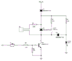
Fig. 1 is a circuit diagram of the present invention.
Detailed Description
The technical solutions in the embodiments of the present invention will be described clearly and completely with reference to the accompanying drawings in the embodiments of the present invention, and it is obvious that the described embodiments are only some embodiments of the present invention, not all embodiments. Based on the embodiments in the present invention, all other embodiments obtained by a person skilled in the art without creative work belong to the protection scope of the present invention.
Referring to fig. 1, IN an embodiment of the present invention, an external load operation indicating circuit includes a diode D1, a resistor R1, a switch S1, a transistor TR1, a light emitting diode LED1 and a light emitting diode LED2, an anode of the diode D1 is connected to a power supply BAT _ IN, a cathode of the diode D1 is connected to cathodes of a resistor R1, a resistor R2, a resistor R3 and a diode D2, respectively, an other end of the resistor R1 is connected to an anode of the light emitting diode LED1, a cathode of the light emitting diode LED1 is connected to a cathode of the diode D1, an anode of the diode D1, a collector of the transistor TR1 and a pin of the external load connector B1, another pin of the external load connector B1 is connected to the other end of the resistor R1, an anode of the diode D1 is connected to the other end of the resistor R1 and an anode of the grounded light emitting diode LED1, an emitter of the transistor TR1 is connected to the resistor R1 and a base of, the other end of the resistor R4 is connected to a power supply VCC through a switch D1.
In the figure, B1 is an external load connector, a switch S1 is a soft touch key, a triode TR1 is used as an electronic switch, and LEDs 1 and 2 are indicating lamps, wherein a light emitting diode LED1 is a green light emitting diode, a light emitting diode LED2 is a red light emitting diode, D1 is an anti-reverse diode, D2 is a freewheeling diode, D3 is a clamp diode, and resistors R1, R2 and R3 are current limiting resistors.
After the external load connector B1 is connected with a resistive load or an inductive load, the key switch S1 is pressed, the triode TR1 is IN saturated conduction, the power supply BAT _ IN supplies power to the load through the diode D1, and the load works normally. In addition, due to the conduction of the transistor TR1, the green indicator light LED1 and the R1 are connected to the ground, the indicator light LED1 is turned on to indicate that the load works normally, and at the moment, the red indicator light LED2 is not turned on, because the voltage of the collector of the TR1 is close to 0V after the transistor TR1 is conducted in a saturated mode, the voltage of the red indicator light LED2 is clamped to be about 1V through the clamping diode D3, and the LED2 cannot be turned on sufficiently. When the key switch S1 is pressed again, the switch is turned off, the transistor TR1 is not conducted, in the other circuit, the diode D3 is reversely connected and is not conducted, so that the green light-emitting diode LED1 is turned off, and the red light-emitting diode LED2 is not clamped at 1V by the diode due to the non-conduction of the transistor TR1, so that the LED2 is turned on, and the indicating load does not work at the moment.
To sum up, the utility model discloses external load work indicating circuit can be used for detecting the quality that the perception is responsible for and hindering nature load, when inserting the utility model discloses when the external load of circuit is not unusual, green emitting diode LED1 in this circuit lights, and it is unusual to indicate the load, when inserting the utility model discloses when the external load of circuit exists unusually, red emitting diode LED2 in this circuit lights, and it is unusual to indicate the load, and circuit structure is simple, low cost.
It is obvious to a person skilled in the art that the invention is not restricted to details of the above-described exemplary embodiments, but that it can be implemented in other specific forms without departing from the spirit or essential characteristics of the invention. The present embodiments are therefore to be considered in all respects as illustrative and not restrictive, the scope of the invention being indicated by the appended claims rather than by the foregoing description, and all changes which come within the meaning and range of equivalency of the claims are therefore intended to be embraced therein. Any reference sign in a claim should not be construed as limiting the claim concerned.
Furthermore, it should be understood that although the present description refers to embodiments, not every embodiment may contain only a single embodiment, and such description is for clarity only, and those skilled in the art should integrate the description, and the embodiments may be combined as appropriate to form other embodiments understood by those skilled in the art.
Claims (7)
1. An external load work indicating circuit is characterized by comprising a diode D1, a resistor R1, a switch S1, a triode TR1, a light emitting diode LED1 and a light emitting diode LED2, the anode of the diode D1 is connected with a power supply BAT _ IN, the cathode of the diode D1 is respectively connected with the cathodes of the resistors R1, R2, R3 and D2, the other end of the resistor R1 is connected with the anode of the light emitting diode LED1, the cathode of the light emitting diode LED1 is respectively connected with the cathode of the diode D3, the anode of the diode D2, the collector of the triode TR1 and one pin of an external load connector B1, the other pin of the external load connector B1 is connected with the other end of the resistor R3, the anode of the diode D3 is respectively connected with the other end of the resistor R2 and the anode of the grounding light emitting diode LED2, the emitter of the triode TR1 is connected with the resistor R5 and is grounded, the other end of the resistor R5 is respectively connected with the base of the triode TR1 and the resistor R4, and the other end of the resistor R4 is connected with a power supply VCC through a switch D1.
2. The external load operation indicating circuit according to claim 1, wherein the transistor TR1 is an NPN transistor.
3. The external load operation indicating circuit of claim 2, wherein the LED1 is a green LED.
4. The external load operation indicating circuit of claim 3, wherein the LED2 is a red LED.
5. The external load operation indicating circuit according to claim 4, wherein the VCC voltage is 5V.
6. The external load operation indicating circuit according to claim 5, wherein the transistor TR1 is MMBT 5551.
7. The external load operation indicating circuit according to any one of claims 1 to 6, wherein the switch D1 is a key switch.
Priority Applications (1)
| Application Number | Priority Date | Filing Date | Title |
|---|---|---|---|
| CN202021349876.4U CN212910129U (en) | 2020-07-10 | 2020-07-10 | External load work indicating circuit |
Applications Claiming Priority (1)
| Application Number | Priority Date | Filing Date | Title |
|---|---|---|---|
| CN202021349876.4U CN212910129U (en) | 2020-07-10 | 2020-07-10 | External load work indicating circuit |
Publications (1)
| Publication Number | Publication Date |
|---|---|
| CN212910129U true CN212910129U (en) | 2021-04-06 |
Family
ID=75284777
Family Applications (1)
| Application Number | Title | Priority Date | Filing Date |
|---|---|---|---|
| CN202021349876.4U Active CN212910129U (en) | 2020-07-10 | 2020-07-10 | External load work indicating circuit |
Country Status (1)
| Country | Link |
|---|---|
| CN (1) | CN212910129U (en) |
Cited By (1)
| Publication number | Priority date | Publication date | Assignee | Title |
|---|---|---|---|---|
| CN115904851A (en) * | 2023-01-10 | 2023-04-04 | 荣耀终端有限公司 | Terminal equipment and external equipment access detection system |
-
2020
- 2020-07-10 CN CN202021349876.4U patent/CN212910129U/en active Active
Cited By (2)
| Publication number | Priority date | Publication date | Assignee | Title |
|---|---|---|---|---|
| CN115904851A (en) * | 2023-01-10 | 2023-04-04 | 荣耀终端有限公司 | Terminal equipment and external equipment access detection system |
| CN115904851B (en) * | 2023-01-10 | 2023-08-15 | 荣耀终端有限公司 | Terminal equipment and external equipment access detection system |
Similar Documents
| Publication | Publication Date | Title |
|---|---|---|
| CN110769564B (en) | Circuit capable of automatically adjusting output current along with input voltage and LED driving power supply | |
| CN212910129U (en) | External load work indicating circuit | |
| CN201277999Y (en) | Positive and negative wave form detection circuit for electric grid and refrigerator with such circuit | |
| CN209878946U (en) | Mainboard detection circuit | |
| CN106199146B (en) | electroscope | |
| CN204349330U (en) | Self-check type state indicator | |
| CN203772299U (en) | Thru-beam sensor detection device | |
| CN110703154A (en) | Socket test circuit and broadcast control method for socket test | |
| CN203950450U (en) | A kind of solution conductivity display | |
| CN1124493C (en) | Chargeable cell test loop contact resistance monitoring method | |
| CN209765005U (en) | flight parameter collector switch quantity testing device | |
| CN218481578U (en) | Test pencil | |
| CN214150904U (en) | Electronic paper module testing jig with programmable driving voltage | |
| CN219266402U (en) | Alternating current/direct current dual-purpose ammeter circuit | |
| CN1892233A (en) | Optical-coupling amplifying type electronic test pencil | |
| CN211086507U (en) | Batch nixie tube detection device | |
| CN212134872U (en) | IGBT fault diagnosis device | |
| CN210958871U (en) | Comprehensive performance tester for electronic ballast | |
| CN217385635U (en) | Single lamp test pencil circuit and test pencil | |
| CN211603518U (en) | Multi-core cable detection device | |
| CN204760345U (en) | Fuse supervisory circuits | |
| CN216792420U (en) | Wire harness detection device based on LED lamp | |
| CN215067216U (en) | Cable detection tool plate circuit | |
| CN219068421U (en) | 0-10V dimming constant current source circuit allowing mains supply to be connected | |
| CN218767077U (en) | Universal voltage test board circuit |
Legal Events
| Date | Code | Title | Description |
|---|---|---|---|
| GR01 | Patent grant | ||
| GR01 | Patent grant |