CN210780675U - Novel axial diode resistance welding junction box - Google Patents
Novel axial diode resistance welding junction box Download PDFInfo
- Publication number
- CN210780675U CN210780675U CN201921816898.4U CN201921816898U CN210780675U CN 210780675 U CN210780675 U CN 210780675U CN 201921816898 U CN201921816898 U CN 201921816898U CN 210780675 U CN210780675 U CN 210780675U
- Authority
- CN
- China
- Prior art keywords
- terminal
- axial diode
- box
- resistance welding
- diode
- Prior art date
- Legal status (The legal status is an assumption and is not a legal conclusion. Google has not performed a legal analysis and makes no representation as to the accuracy of the status listed.)
- Active
Links
Images


Classifications
-
- Y—GENERAL TAGGING OF NEW TECHNOLOGICAL DEVELOPMENTS; GENERAL TAGGING OF CROSS-SECTIONAL TECHNOLOGIES SPANNING OVER SEVERAL SECTIONS OF THE IPC; TECHNICAL SUBJECTS COVERED BY FORMER USPC CROSS-REFERENCE ART COLLECTIONS [XRACs] AND DIGESTS
- Y02—TECHNOLOGIES OR APPLICATIONS FOR MITIGATION OR ADAPTATION AGAINST CLIMATE CHANGE
- Y02E—REDUCTION OF GREENHOUSE GAS [GHG] EMISSIONS, RELATED TO ENERGY GENERATION, TRANSMISSION OR DISTRIBUTION
- Y02E10/00—Energy generation through renewable energy sources
- Y02E10/50—Photovoltaic [PV] energy
Abstract
The utility model provides a novel axial diode resistance welding junction box, which comprises a box body and a box cover matched with the upper edge of the box body, wherein an axial diode and a plurality of terminal pieces electrically connected through the diode are arranged in the box body; the terminal plate is provided with axial diode wire holders, pins on two sides of each axial diode are respectively welded and fixed with two adjacent axial diode wire holders in a resistance welding mode, and the axial diodes are connected with the terminal plate to form a whole. The utility model discloses a novel axial diode resistance welds terminal box through optimizing terminal box configuration device, makes whole overcurrent ability strengthen by a wide margin, and diode heat-sinking capability greatly increased is fit for high-power component and uses, compact structure, and the aesthetic property has also obtained the promotion.
Description
Technical Field
The utility model relates to a solar photovoltaic technical field especially relates to a photovoltaic module is with novel axial diode resistance welding terminal box.
Background
The solar photovoltaic module is a device for converting solar energy into electric energy, and when the solar photovoltaic module is used, the electric energy generated by the photovoltaic module needs to be led out by using the junction box of the photovoltaic module.
In the prior art, a common photovoltaic junction box includes a box body and a plurality of conductors (conductive terminals) installed in the box body and electrically connected to a module bus bar, and bypass diodes are connected between the conductors. Most of the diodes used in the current photovoltaic module junction box are of a patch structure, and the diodes of the structure have the advantages of small area, no pins, small occupied installation space and suitability for small-size junction boxes; meanwhile, the patch diode is also particularly insufficient, for example, the connection mode between the patch diode and the conductor (generally, a copper sheet) is mostly soldering, the connection mode has high requirement on equipment, large investment, inconvenient processing, most of the processes are complicated, the processing efficiency is low, the manufacturing cost is high, and the manufacturing cost of the junction box is seriously influenced.
In addition, the bypass diode has larger heat productivity in the working process of the junction box, and the patch diode with smaller volume has weaker over-current capability, so that the junction box is not suitable for the application requirement of the popular high-power photovoltaic module at present.
SUMMERY OF THE UTILITY MODEL
To the technical problem, an object of the utility model is to provide a novel axial diode resistance welds terminal box, cross the electric capacity reinforce, production technology is comparatively simple, and the diode heat-sinking capability is strong and can reduce cost.
In order to achieve the above purpose, the utility model discloses a following technical scheme realizes:
a novel axial diode resistance welding junction box comprises a box body and a box cover matched with the box body, wherein a plurality of bus bar connecting terminal pieces are arranged in the box body, and adjacent terminal pieces are electrically connected through an axial diode; the terminal pieces are provided with axial diode wire holders, and pins on two sides of an axial diode are respectively welded and fixed with the axial diode wire holders on two adjacent terminal pieces in a resistance welding mode; wiring parts which are fixedly connected with the cable are arranged on two sides in the wiring box, and the wiring parts are in a U-shaped groove structure; an electric isolation column is arranged between adjacent terminal pieces in the box body, and a solar cell bus bar connecting area and a bus bar leading-out groove are arranged on the terminal pieces.
Preferably, a pair of bending parts perpendicular to the plane of the terminal plate is arranged at the joint of the terminal plate and the axial diode, and a notch for placing a pin of the axial diode is arranged between the pair of bending parts.
Preferably, the U-shaped groove is designed in a two-section mode, and an opening is formed in the middle of the U-shaped groove.
Preferably, the head of the cable and the wiring part are connected and fixed in a riveting and ultrasonic welding mode.
Preferably, the two wiring portions are arranged in a splayed shape in the junction box, and the wiring portions on the two sides and the terminal pieces connected with the wiring portions are integrally formed.
Preferably, the connection area is uniformly provided with a plurality of fixed salient points at intervals, so that the bus bars and the connection area can be conveniently connected and fixed through resistance welding.
Preferably, the junction box is provided with three axial diodes, and the three axial diodes are arranged in the junction box in an inverted 'article' shape.
Compared with the prior art, the utility model discloses following beneficial effect has:
(1) the axial diode pin and the terminal piece are connected by resistance welding, the diode pin is tightly attached to the copper plate, and the heat dissipation capability is strong; in the process of resistance welding, the heat is concentrated, the heating time is shortened, the welding deformation is small, the influence on a diode chip is small, meanwhile, the welding part is directly melted and combined, filling materials, solvents and protective gas are not needed, and the welding efficiency is also effectively improved;
(2) the cable connecting part adopts a U-shaped clamping groove structure, the head of the cable is riveted with the buckle of the clamping groove and then welded by ultrasonic wave, and compared with the traditional method of locking the cable by a nut, the method is simpler and more convenient and improves the firmness;
(3) the diode adopts an axial diode and is integrally connected with the terminal plate, so that the integral connection is compact, the volume is saved, and the integral junction box body becomes beautiful and elegant; the overall overcurrent capacity of the junction box is greatly improved; the high-power module is suitable for use requirements of high-power modules.
Drawings
FIG. 1 is a schematic structural view of the interior of the box body of the novel axial diode resistance welding junction box of the present invention;
FIG. 2 is a schematic structural view of the box cover of the novel axial diode resistance welding junction box of the present invention;
fig. 3 is a partially enlarged view of the novel axial diode resistance welding terminal box of the present invention.
Detailed Description
In order to further understand the objects, structures, features and functions of the present invention, the following embodiments are described in detail.
It should be noted that in the description of the present invention, the terms "upper", "left", "right", "inner", "outer", "vertical", "horizontal", etc. indicate the orientation or positional relationship based on the orientation or positional relationship shown in the drawings, which are only for convenience of description and simplification of description, but do not indicate or imply that the device or element referred to must have a specific orientation or be constructed and operated in a specific orientation, and thus, should not be construed as limiting the present invention.
Referring to fig. 1 and 2, the novel axial diode resistance welding junction box of the present embodiment includes a box body 1 and a box cover 2 adapted to the box body 1, wherein a plurality of bus bar connection terminal pieces 5 are disposed in the box body 1, and adjacent terminal pieces 5 are electrically connected through an axial diode 4.
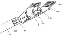
The terminal plate 5 is provided with an axial diode wire holder 501, and the pins on two sides of the axial diode 4 are directly welded and fixed with the axial diode wire holders 501 on two adjacent terminal plates in a resistance welding mode. Compared with the traditional tin soldering type welding, the resistance welding has the advantages that the heat is concentrated in the welding process, the heating time is shortened, the welding deformation is small, the influence on a diode chip is small, meanwhile, the welding part is directly melted and combined, filling materials, solvents and protective gas are not needed, the welding efficiency is effectively improved, and the labor environment is good; the axial diode 4 and the terminal plate 5 are connected to form a whole, the arrangement is compact, the attractiveness of the box body is improved, and the electrical performance of the junction box is greatly improved. Referring to fig. 3, in order to ensure the positioning accuracy during resistance welding of the axial diode, a pair of bending portions 541 and 542 perpendicular to the plane of the terminal piece is arranged at the joint of the terminal piece 5 and the axial diode, and a gap for placing a pin of the axial diode is formed between the pair of bending portions. The axial diode and the copper plate terminal are combined and resistance-welded together, the pin of the diode is tightly attached to the copper plate, the heat dissipation capability is strong, and the heat dissipation device is particularly suitable for the heat dissipation requirement of the junction box of a high-power assembly.
Both sides still are equipped with the wiring portion 32 of being connected fixedly with cable conductor 31 in the terminal box, refer to fig. 3, wiring portion 32 be U type groove structure, just U type groove structure be two segmentation designs, the centre is equipped with opening 321, the head of cable conductor 31 stretches into the U type groove of wiring portion 32 in the box body and connects fixedly through the riveting mode, both conveniently observe the riveting condition of cable conductor through opening 321, it is fixed to make the riveting department divide into two atress evenly simultaneously when the riveting condition is not good, increase the firmness and the reliability of connecting. In a preferred embodiment, the head of the cable 31 is connected with the wire connecting portion 32 by riveting and then ultrasonic welding, so that the firmness is greatly improved, and the cable connector is not easy to rotate or pull out; in a preferred embodiment, referring to fig. 1, two wire connecting portions 32 are disposed in a "v" shape in the junction box, and the wire connecting portions on both sides and the terminal pieces connected to the wire connecting portions are integrally formed.
With reference to fig. 1, an electrical isolation column 6 is further disposed between adjacent terminal pieces in the case 1 for reducing interference between different circuits and protecting the circuits, a solar cell bus bar connection region 503 and a bus bar lead-out groove 504 are further disposed on the terminal piece 5, and a bus bar passes through the lead-out groove 504 and is connected to the connection region 503 by welding, preferably, referring to fig. 3, a plurality of bumps 5031 are disposed at uniform intervals in the connection region 503, so that the bus bar and the connection region 503 are connected and fixed by resistance welding, thereby improving process efficiency and improving working environment.
Preferably, the terminal plate 5 may be a copper plate, and the box body 1 and the box cover 2 are made of a high temperature resistant material, and may be a nylon material.
In a preferred embodiment, three axial diodes 4 are provided in the junction box, in the shape of an inverted "pin" in the junction box.
In an embodiment, a positioning column 502 is further disposed on the base of the box body 1, a positioning hole matched with the positioning column 502 is disposed on the terminal plate 5, and the positioning column 502 passes through the corresponding positioning hole and is fixed to the terminal plate in a self-hot-melting manner.
The junction box of the utility model uses the axial diode, the pin and the terminal plate of the diode can be directly fixed and selected with the resistance welding process with stable performance, the conditions of infirm welding and low efficiency of the diode are reduced, the diode and the copper plate terminal form a whole, and the electrical performance of the junction box is greatly improved; the diode and the copper plate terminal are combined and resistance-welded together, and the pin of the diode is tightly attached to the copper plate, so that the heat dissipation capability is strong; in the welding process, the heat is concentrated, the heating time is short, the welding deformation is small, and the influence on the diode chip is small; the resistance welding mode adopts direct melting combination, does not need filling materials and solvents, does not need protective gas, and has high welding efficiency and good labor environment; the axial diode and the copper plate are connected into a whole, so that the whole connection is compact, the volume is saved, and the whole junction box body is attractive and elegant; the cable conductor wiring portion of terminal box designs into U type draw-in groove structure, and the cable conductor head is riveted earlier with the buckle and is pushed down the cable again to use ultrasonic wave innovation technique, makes the cable not pulled out or rotate, has replaced the loaded down with trivial details connected mode of traditional nut locking cable.
The utility model discloses a novel axial diode resistance welds terminal box through optimizing terminal box configuration device, makes whole overcurrent ability, diode heat-sinking capability greatly increased, and too big electric current ability is stronger, is fit for high-power component and uses, and the aesthetic property has also obtained the promotion.
The present invention has been described in relation to the above embodiments, which are only examples for implementing the present invention. It should be noted that the disclosed embodiments do not limit the scope of the present invention. On the contrary, all changes and modifications which do not depart from the spirit and scope of the present invention are deemed to fall within the scope of the present invention.
Claims (7)
1. The novel axial diode resistance welding junction box is characterized by comprising a box body and a box cover matched with the box body, wherein a plurality of bus bar connecting terminal pieces are arranged in the box body, and adjacent terminal pieces are electrically connected through an axial diode; the terminal pieces are provided with axial diode wire holders, and pins on two sides of an axial diode are respectively welded and fixed with the axial diode wire holders on two adjacent terminal pieces in a resistance welding mode; wiring parts which are fixedly connected with the cable are arranged on two sides in the wiring box, and the wiring parts are in a U-shaped groove structure; an electric isolation column is arranged between adjacent terminal pieces in the box body, and a solar cell bus bar connecting area and a bus bar leading-out groove are arranged on the terminal pieces.
2. The novel axial diode resistance welding junction box as claimed in claim 1, wherein a pair of bending portions perpendicular to the plane of the terminal plate is arranged at the connection part of the terminal plate and the axial diode, and a gap for placing a pin of the axial diode is arranged between the pair of bending portions.
3. The novel axial diode resistance welding terminal block as defined in claim 1 or 2, wherein said U-shaped groove is configured in two-step design with an opening in the middle.
4. The novel axial diode resistance welding terminal box as claimed in claim 3, wherein the head of the cable and the wire connecting portion are connected and fixed in a manner of riveting and then ultrasonic welding.
5. The novel axial diode resistance welding terminal box as claimed in claim 4, wherein the two wiring portions are arranged in a shape of a Chinese character 'ba' in the terminal box, and the wiring portions at both sides and the terminal pieces connected with the wiring portions are integrally formed.
6. The novel axial diode resistance welding terminal block as defined in claim 5, wherein said connection block is provided with a plurality of fixing projections at regular intervals for facilitating the connection of the bus bar and the connection block by resistance welding.
7. The novel axial diode resistance welding terminal box of claim 6, wherein three axial diodes are arranged in the terminal box and are arranged in the shape of an inverted Chinese character 'pin' in the terminal box.
Priority Applications (1)
| Application Number | Priority Date | Filing Date | Title |
|---|---|---|---|
| CN201921816898.4U CN210780675U (en) | 2019-10-28 | 2019-10-28 | Novel axial diode resistance welding junction box |
Applications Claiming Priority (1)
| Application Number | Priority Date | Filing Date | Title |
|---|---|---|---|
| CN201921816898.4U CN210780675U (en) | 2019-10-28 | 2019-10-28 | Novel axial diode resistance welding junction box |
Publications (1)
| Publication Number | Publication Date |
|---|---|
| CN210780675U true CN210780675U (en) | 2020-06-16 |
Family
ID=71041990
Family Applications (1)
| Application Number | Title | Priority Date | Filing Date |
|---|---|---|---|
| CN201921816898.4U Active CN210780675U (en) | 2019-10-28 | 2019-10-28 | Novel axial diode resistance welding junction box |
Country Status (1)
| Country | Link |
|---|---|
| CN (1) | CN210780675U (en) |
-
2019
- 2019-10-28 CN CN201921816898.4U patent/CN210780675U/en active Active
Similar Documents
| Publication | Publication Date | Title |
|---|---|---|
| CN216288418U (en) | Improved shaft type diode, bypass module using same and photovoltaic module junction box | |
| CN103413852B (en) | The solar junction box of card welding end minor structure | |
| CN210780675U (en) | Novel axial diode resistance welding junction box | |
| CN216671617U (en) | Diode module for junction box free of copper plate welding and junction box using diode module | |
| CN110855236A (en) | Novel axial diode resistance welding junction box | |
| CN216819794U (en) | Full-glue-pouring split type photovoltaic junction box and photovoltaic cell assembly | |
| CN111769798A (en) | Improved modularized photovoltaic assembly bypass element and assembly junction box | |
| CN212086155U (en) | Junction box with diode side-discharge heat-radiating device | |
| CN112994611A (en) | Low-cost large-current split type photovoltaic module junction box | |
| CN210110743U (en) | Bypass diode frame and monomer bypass diode | |
| CN209964015U (en) | Junction box for power generation of high-power high-efficiency photovoltaic module | |
| CN212305259U (en) | Improved modularized photovoltaic assembly bypass element and assembly junction box | |
| CN209401707U (en) | A kind of special fixture of no mould group class aluminum-shell battery mould group | |
| CN219227545U (en) | Three-split photovoltaic wiring device for double-glass assembly | |
| CN203288622U (en) | Photovoltaic wiring box with improved box body structure | |
| CN217428079U (en) | Split type terminal box soaks in bottom | |
| CN214591313U (en) | Low-cost split type photovoltaic module junction box adopting axial diodes | |
| CN215934812U (en) | Bypass module for high-current junction box with good heat dissipation performance and junction box with bypass module | |
| CN212783439U (en) | High current-carrying modularized photovoltaic assembly bypass element and junction box | |
| CN219420718U (en) | Electric conduction heat conduction piece and photovoltaic junction box thereof | |
| CN214898430U (en) | Bipartite solar junction box and conductive module diode thereof | |
| CN218868195U (en) | Plug-in box cover of photovoltaic junction box | |
| CN220022746U (en) | Junction box structure | |
| CN213071116U (en) | Improved modular photovoltaic module bypass element and module junction box | |
| CN217984995U (en) | Pen-shaped split junction box |
Legal Events
| Date | Code | Title | Description |
|---|---|---|---|
| GR01 | Patent grant | ||
| GR01 | Patent grant |