CN210405093U - Audio band noise elimination circuit applied to voltage reduction DCDC converter - Google Patents
Audio band noise elimination circuit applied to voltage reduction DCDC converter Download PDFInfo
- Publication number
- CN210405093U CN210405093U CN201921436785.1U CN201921436785U CN210405093U CN 210405093 U CN210405093 U CN 210405093U CN 201921436785 U CN201921436785 U CN 201921436785U CN 210405093 U CN210405093 U CN 210405093U
- Authority
- CN
- China
- Prior art keywords
- electrically connected
- pwm
- sampling
- ldo
- output
- Prior art date
- Legal status (The legal status is an assumption and is not a legal conclusion. Google has not performed a legal analysis and makes no representation as to the accuracy of the status listed.)
- Active
Links
Images
Abstract
The utility model relates to a lithium cell management technical field that discharges especially relates to an audio frequency band noise elimination circuit who is applied to step-down DCDC converter. The power supply circuit comprises a power supply end, a load end, a PWM control loop, an LDO control loop and a power output part, wherein the PWM control loop, the LDO control loop and the power output part are arranged between the power supply end and the load end; the power output part comprises a first input end, a voltage output end and a PWM input end, the first input end is electrically connected with the power supply end, the voltage output end is electrically connected with the load end, and the voltage output end is also connected with a sampling resistor; the PWM control loop comprises a first sampling end and a PWM output end, the first sampling end is electrically connected with the sampling resistor, and the PWM output end is electrically connected with the PWM input end; the LDO control loop comprises a second input end, a second sampling end and an LDO output end, the second input end is electrically connected with the power supply end, the second sampling end is electrically connected with the sampling resistor, and the LDO output end is electrically connected with the voltage output end. The utility model discloses with LDO mode operation when the load alleviates, can not produce the noise of audio frequency band when the load alleviates.
Description
Technical Field
The utility model relates to a lithium cell management technical field that discharges especially relates to an audio frequency band noise elimination circuit who is applied to step-down DCDC converter.
Background
With the popularization of lithium batteries, people have higher and higher requirements on lithium battery discharge management. In some audio devices applied to lithium batteries, such as microphones and interphones, on-chip DCDC converters mostly adopt a PWM/PFM switching mode, although the conversion efficiency of a power supply system under light load can be effectively improved, when the load is changed from heavy load to light load, that is, when the PFM mode is adopted, the switching frequency of the DCDC converter can be reduced from several megahertz to several kilohertz or even several hertz, so that the switching frequency of the DCDC converter can fall into an audio frequency band under light load, and further noise is generated.
SUMMERY OF THE UTILITY MODEL
To the technical problem of prior art, the utility model provides an audio frequency band noise elimination circuit and method for step-down DCDC converter.
In order to solve the technical problem, the utility model provides a following technical scheme:
an audio band noise elimination circuit applied to a buck DCDC converter comprises a power supply end, a load end, a PWM control loop, an LDO control loop and a power output part, wherein the PWM control loop, the LDO control loop and the power output part are arranged between the power supply end and the load end; the power output part comprises a first input end, a voltage output end and a PWM input end, the first input end is electrically connected with the power supply end, the voltage output end is electrically connected with the load end, and the voltage output end is also connected with a sampling resistor; the PWM control loop comprises a first sampling end and a PWM output end, the first sampling end is electrically connected with the sampling resistor, and the PWM output end is electrically connected with the PWM input end; the LDO control loop comprises a second input end, a second sampling end and an LDO output end, the second input end is electrically connected with the power supply end, the second sampling end is electrically connected with the sampling resistor, and the LDO output end is electrically connected with the voltage output end.
When the circuit is powered on, the circuit enables the LDO control loop by default, namely, the circuit runs in the LDO mode. PWM control circuit, LDO control circuit are connected with the sampling resistor electricity through first sample terminal, second sample terminal respectively to the change of the output voltage of voltage output end is acquireed in real time with the voltage variation through the sampling resistor, and then the change of load on the real-time acquisition load end. When the load is heavier, the output voltage is reduced, the PWM control loop detects the change of the load through the first sampling end, so that the whole functions of the PWM control loop are started to enable a PWM mode, and at the moment, the circuit runs in a mode of mixing PWM and LDO to bear the heavier load. When the load is relieved, the output voltage rises, and the PWM control loop detects the change of the load, so that other functions of the PWM control loop are closed to close the PWM mode, and the circuit runs in the LDO mode. In summary, the circuit can automatically switch between two operation modes to adapt to different loads, wherein the LDO mode does not include a switching action and belongs to a linear power supply, and therefore, when the load is relieved, the switching noise falling into an audio frequency band is not generated.
Further, the power output part further comprises a first power tube, an inductor and an output capacitor which are arranged among the first input end, the PWM input end and the voltage output end; two ends of the inductor are respectively and electrically connected with the D pole of the first power tube and the output capacitor; the S pole of the first power tube is electrically connected with the first input end, the G pole of the first power tube is electrically connected with the PWM input end, and the D pole of the first power tube is also connected with a synchronous rectifier tube; the output capacitor is electrically connected with the voltage output end.
Furthermore, the PWM control loop further includes an oscillator, a logic circuit, a logic control driving circuit, and a PWM comparator, which are disposed between the PWM output terminal and the first sampling terminal; the logic circuit is electrically connected with the oscillator, the logic control driving circuit and the PWM comparator; the PWM comparator is electrically connected with the first sampling end and is also connected with a first reference voltage group; and the logic control driving circuit is electrically connected with the PWM output end.
Further, an output electrode of the PWM comparator is electrically connected to the logic circuit, a negative electrode of the PWM comparator is electrically connected to the first sampling terminal, and a positive electrode of the PWM comparator is electrically connected to the first reference voltage group.
Further, a timer is arranged in the logic circuit.
Further, the LDO control loop includes an operational amplifier and a second power tube disposed between the second input terminal, the second sampling terminal, and the LDO output terminal; the S pole of the second power tube is electrically connected with the second input end, the D pole of the second power tube is electrically connected with the output end of the LDO, and the G pole of the second power tube is electrically connected with the operational amplifier; the operational amplifier is electrically connected with the second sampling end, and a second reference voltage group is further connected to the operational amplifier.
Further, the output electrode of the operational amplifier is electrically connected with the G electrode of the second power tube, the negative electrode of the operational amplifier is electrically connected with the second sampling end, and the positive electrode of the operational amplifier is electrically connected with the second reference voltage group.
Further, the sampling resistor comprises a first resistor and a second resistor, and the first resistor is connected with the second resistor in series; the first sampling end is connected between the first resistor and the second resistor, and the second sampling end is connected between the first resistor and the second resistor.
Compared with the prior art, the utility model has the advantages of it is following:
when the circuit is powered on, the circuit is operated in an LDO mode by default. When the load aggravates, this circuit moves with LDO/PWM mixed mode, if the load alleviates this moment, this circuit can automatic switch over to the LDO mode, wherein, the LDO mode does not include the switching action, belongs to linear power for this circuit can not produce the switching noise that falls into the audio frequency band when the load alleviates.
Drawings
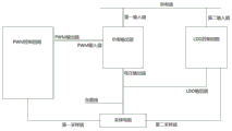
FIG. 1: the overall structure of the circuit.
FIG. 2: and a circuit component connection diagram.
Detailed Description
The following are specific embodiments of the present invention and the accompanying drawings are used to further describe the technical solution of the present invention, but the present invention is not limited to these embodiments.
An audio band noise elimination circuit applied to a buck DCDC converter comprises a power supply end, a load end, a PWM control loop, an LDO control loop and a power output part, wherein the PWM control loop, the LDO control loop and the power output part are arranged between the power supply end and the load end.
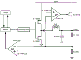
The power output part comprises a first input end, a voltage output end and a PWM input end, the first input end is electrically connected with the power supply end, the voltage output end is electrically connected with the load end, the voltage output end is further connected with a sampling resistor, the sampling resistor comprises a first resistor and a second resistor, one end of the first resistor is electrically connected with the voltage output end, the other end of the first resistor is electrically connected with the second resistor, and the second resistor is further provided with a grounding end. The power output part also comprises a first power tube, an inductor and an output capacitor which are arranged among the first input end, the PWM input end and the voltage output end; two ends of the inductor are respectively and electrically connected with a D pole of the first power tube and the output capacitor; the S pole of the first power tube is electrically connected with the first input end, the G pole of the first power tube is electrically connected with the PWM input end, the D pole of the first power tube is also electrically connected with the D pole of the synchronous rectifying tube, the G pole of the synchronous rectifying tube is electrically connected with the PWM input end, and the S pole of the synchronous rectifying tube is provided with a grounding end. One end of the output capacitor is electrically connected with the voltage output end, and the other end of the output capacitor is provided with a grounding end.
The PWM control loop comprises a first sampling end and a PWM output end, the first sampling end is connected between the first resistor and the second resistor, and the PWM output end is electrically connected with the PWM input end. The PWM control loop also comprises an oscillator, a logic circuit, a logic control driving circuit and a PWM comparator which are arranged between the PWM output end and the first sampling end; the logic circuit is electrically connected with the oscillator, the logic control driving circuit and the output electrode of the PWM comparator, a timer is arranged in the logic circuit, set time is stored in the logic circuit, the negative electrode of the PWM comparator is electrically connected with the first sampling end, and the positive electrode of the PWM comparator is electrically connected with the first reference voltage group; the logic control drive circuit is electrically connected with the PWM output end.
The LDO control loop comprises a second input end, a second sampling end and an LDO output end, and the second sampling end is connected between the first resistor and the second resistor. The second sampling end is electrically connected with the sampling resistor, and the LDO output end is electrically connected with the voltage output end. The LDO control loop comprises an operational amplifier and a second power tube, wherein the operational amplifier and the second power tube are arranged among a second input end, a second sampling end and an LDO output end; the S pole of the second power tube is electrically connected with the second input end, the D pole of the second power tube is electrically connected with the output end of the LDO, and the G pole of the second power tube is electrically connected with the output end of the operational amplifier; the negative electrode of the operational amplifier is electrically connected with the second sampling end, and the positive electrode of the operational amplifier is electrically connected with the second reference voltage group.
In actual use, supply power to first input, second input through the supply end for LDO control loop gets electric, and then operates LDO control loop, makes this circuit operate with the LDO mode. The circuit outputs voltage to a load end through a voltage output end arranged on the power output part so as to bear load. Under the influence of the load on the load terminal, the output voltage on the voltage output terminal will float with the change of the load, and the floating of the output voltage will reflect the change of the load. The boundary value of output voltage floating is set by the first reference voltage group connected to the positive pole of the PWM comparator and the second reference voltage group connected to the positive pole of the operational amplifier, namely the minimum set voltage and the maximum set voltage are set by the cooperation of the first reference voltage group and the second reference voltage group. The negative pole of the PWM comparator is electrically connected with the first sampling end, so that the voltage of the sampling resistor is obtained in real time, the output voltage of the voltage output end is obtained in real time, the PWM comparator compares the output voltage with the minimum set voltage and the maximum set voltage respectively, the floating state of the output voltage is obtained according to the comparison result, and the change of the load is judged.
When the load is aggravated, the output voltage is reduced, so that the output voltage is smaller than the minimum set voltage, at the moment, the PWM comparator is overturned, the output electrode of the PWM comparator outputs high level, the oscillator, the logic circuit and the logic control driving circuit are started, all functions of the PWM control loop are started to enable the PWM mode, the circuit is enabled to operate in a mode of mixing LDO/PWM, and the circuit can bear the aggravated load.
When the circuit operates in the LDO/PWM mixed mode, if the load is lightened, the output voltage is increased, so that the output voltage is larger than the maximum set voltage, at the moment, the turnover of the PWM comparator disappears, the output pole of the PWM comparator outputs low level, the timer in the logic circuit starts to time, when the PWM comparator turns over again, namely the load is aggravated again, the timer stops timing, the current timing duration is cleared, and the circuit continues to operate in the LDO/PWM mixed mode. When the timing duration is equal to the set timing duration, namely the PWM comparator does not overturn again, the output pole of the PWM comparator continuously outputs low level so as to close the oscillator, the logic circuit and the logic control driving circuit, and the circuit runs in the LDO mode. The LDO control loop does not comprise switching action and belongs to a linear power supply, namely, the circuit can not generate switching noise falling into an audio band when running in an LDO mode.
To sum up, the utility model discloses can accomplish the automatic switching between LDO mode, LDO/PWM mixed mode automatically according to the change of load, and make this circuit can not produce the switching noise that falls into the audio frequency band when the load alleviates through the characteristic that utilizes LDO control loop.
The specific embodiments described herein are merely illustrative of the spirit of the invention. Various modifications, additions and substitutions for the specific embodiments described herein may be made by those skilled in the art without departing from the spirit of the invention or exceeding the scope of the invention as defined in the accompanying claims.
Claims (8)
1. An audio band noise cancellation circuit for a buck DCDC converter, comprising: the power supply circuit comprises a power supply end, a load end, a PWM control loop, an LDO control loop and a power output part, wherein the PWM control loop, the LDO control loop and the power output part are arranged between the power supply end and the load end;
the power output part comprises a first input end, a voltage output end and a PWM input end, the first input end is electrically connected with the power supply end, the voltage output end is electrically connected with the load end, and the voltage output end is also connected with a sampling resistor;
the PWM control loop comprises a first sampling end and a PWM output end, the first sampling end is electrically connected with the sampling resistor, and the PWM output end is electrically connected with the PWM input end;
the LDO control loop comprises a second input end, a second sampling end and an LDO output end, the second input end is electrically connected with the power supply end, the second sampling end is electrically connected with the sampling resistor, and the LDO output end is electrically connected with the voltage output end.
2. The audio band noise cancellation circuit applied to a buck DCDC converter as claimed in claim 1, wherein: the power output part also comprises a first power tube, an inductor and an output capacitor which are arranged among the first input end, the PWM input end and the voltage output end;
two ends of the inductor are respectively and electrically connected with the D pole of the first power tube and the output capacitor;
the S pole of the first power tube is electrically connected with the first input end, the G pole of the first power tube is electrically connected with the PWM input end, and the D pole of the first power tube is also connected with a synchronous rectifier tube;
the output capacitor is electrically connected with the voltage output end.
3. The audio band noise cancellation circuit applied to a buck DCDC converter as claimed in claim 1, wherein: the PWM control loop also comprises an oscillator, a logic circuit, a logic control driving circuit and a PWM comparator which are arranged between the PWM output end and the first sampling end;
the logic circuit is electrically connected with the oscillator, the logic control driving circuit and the PWM comparator;
the PWM comparator is electrically connected with the first sampling end and is also connected with a first reference voltage group;
and the logic control driving circuit is electrically connected with the PWM output end.
4. The audio band noise cancellation circuit applied to a buck DCDC converter as claimed in claim 3, wherein: the output electrode of the PWM comparator is electrically connected with the logic circuit, the negative electrode of the PWM comparator is electrically connected with the first sampling end, and the positive electrode of the PWM comparator is electrically connected with the first reference voltage group.
5. The audio band noise cancellation circuit applied to a buck DCDC converter as claimed in claim 3, wherein: and a timer is arranged in the logic circuit.
6. The audio band noise cancellation circuit applied to a buck DCDC converter as claimed in claim 1, wherein: the LDO control loop comprises an operational amplifier and a second power tube which are arranged among the second input end, the second sampling end and the LDO output end;
the S pole of the second power tube is electrically connected with the second input end, the D pole of the second power tube is electrically connected with the output end of the LDO, and the G pole of the second power tube is electrically connected with the operational amplifier;
the operational amplifier is electrically connected with the second sampling end, and a second reference voltage group is further connected to the operational amplifier.
7. The audio band noise cancellation circuit applied to the buck DCDC converter according to claim 6, wherein: the output electrode of the operational amplifier is electrically connected with the G electrode of the second power tube, the negative electrode of the operational amplifier is electrically connected with the second sampling end, and the positive electrode of the operational amplifier is electrically connected with the second reference voltage group.
8. The audio band noise cancellation circuit applied to a buck DCDC converter as claimed in claim 1, wherein: the sampling resistor comprises a first resistor and a second resistor, and the first resistor is connected with the second resistor in series;
the first sampling end is connected between the first resistor and the second resistor, and the second sampling end is connected between the first resistor and the second resistor.
Priority Applications (1)
| Application Number | Priority Date | Filing Date | Title |
|---|---|---|---|
| CN201921436785.1U CN210405093U (en) | 2019-09-02 | 2019-09-02 | Audio band noise elimination circuit applied to voltage reduction DCDC converter |
Applications Claiming Priority (1)
| Application Number | Priority Date | Filing Date | Title |
|---|---|---|---|
| CN201921436785.1U CN210405093U (en) | 2019-09-02 | 2019-09-02 | Audio band noise elimination circuit applied to voltage reduction DCDC converter |
Publications (1)
| Publication Number | Publication Date |
|---|---|
| CN210405093U true CN210405093U (en) | 2020-04-24 |
Family
ID=70340327
Family Applications (1)
| Application Number | Title | Priority Date | Filing Date |
|---|---|---|---|
| CN201921436785.1U Active CN210405093U (en) | 2019-09-02 | 2019-09-02 | Audio band noise elimination circuit applied to voltage reduction DCDC converter |
Country Status (1)
| Country | Link |
|---|---|
| CN (1) | CN210405093U (en) |
Cited By (1)
| Publication number | Priority date | Publication date | Assignee | Title |
|---|---|---|---|---|
| CN110518798A (en) * | 2019-09-02 | 2019-11-29 | 嘉兴飞童电子科技有限公司 | A kind of voiced band noise canceller circuit and method applied to step-down DC/DC converter |
-
2019
- 2019-09-02 CN CN201921436785.1U patent/CN210405093U/en active Active
Cited By (1)
| Publication number | Priority date | Publication date | Assignee | Title |
|---|---|---|---|---|
| CN110518798A (en) * | 2019-09-02 | 2019-11-29 | 嘉兴飞童电子科技有限公司 | A kind of voiced band noise canceller circuit and method applied to step-down DC/DC converter |
Similar Documents
| Publication | Publication Date | Title |
|---|---|---|
| Chuang | High-efficiency ZCS buck converter for rechargeable batteries | |
| TWI221695B (en) | Uninterruptible power system | |
| US20090079385A1 (en) | Solar powered battery charger using switch capacitor voltage converters | |
| Kushwaha et al. | Design and development of modified BL Luo converter for PQ improvement in EV charger | |
| Chuang et al. | Implementation and analysis of an improved series-loaded resonant DC–DC converter operating above resonance for battery chargers | |
| US11588406B2 (en) | Battery charging circuit and battery charging method | |
| CN1402901A (en) | Battery pack | |
| CN207269198U (en) | A kind of high-gain Double-input direct-current converter based on capacitance series parallel structure | |
| CN112909722A (en) | High-power pulse laser power supply circuit | |
| CN202949266U (en) | Intelligent charger | |
| CN105939112A (en) | High-gain quasi-switch boost DC-DC converter | |
| CN105939107A (en) | Hybrid type quasi-switch voltage-boosting DC-DC converter | |
| Gumera et al. | Design and implementation of a high efficiency cost effective EV charger using LLC resonant converter | |
| CN203840049U (en) | Power storage system, charging and discharging circuit, and grid-connected device | |
| CN210405093U (en) | Audio band noise elimination circuit applied to voltage reduction DCDC converter | |
| CN103855779A (en) | Intelligent charger | |
| CN104270085A (en) | DC/DC conversion circuit in solar photovoltaic power generation system | |
| Chuang et al. | Battery float charge technique using parallel-loaded resonant converter for discontinuous conduction operation | |
| CN214798998U (en) | Energy storage device with high-frequency isolation function | |
| CN210490543U (en) | Multi-stage energy storage element parallel charging and discharging system | |
| US20210391796A1 (en) | Battery Path Impedance Compensation | |
| CN211579680U (en) | Lithium battery direct-current power supply system | |
| CN202652074U (en) | DC/DC converter based on LLC resonance | |
| CN205847090U (en) | A kind of mixed type quasi-boost switching DC DC changer | |
| CN100499950C (en) | Self-adaptive output white light LED driver |
Legal Events
| Date | Code | Title | Description |
|---|---|---|---|
| GR01 | Patent grant | ||
| GR01 | Patent grant |