CN202495873U - Power supply circuit and television - Google Patents
Power supply circuit and television Download PDFInfo
- Publication number
- CN202495873U CN202495873U CN2012200963000U CN201220096300U CN202495873U CN 202495873 U CN202495873 U CN 202495873U CN 2012200963000 U CN2012200963000 U CN 2012200963000U CN 201220096300 U CN201220096300 U CN 201220096300U CN 202495873 U CN202495873 U CN 202495873U
- Authority
- CN
- China
- Prior art keywords
- circuit
- power supply
- supply circuit
- resistor
- standby
- Prior art date
- Legal status (The legal status is an assumption and is not a legal conclusion. Google has not performed a legal analysis and makes no representation as to the accuracy of the status listed.)
- Expired - Lifetime
Links
Images


Classifications
-
- Y—GENERAL TAGGING OF NEW TECHNOLOGICAL DEVELOPMENTS; GENERAL TAGGING OF CROSS-SECTIONAL TECHNOLOGIES SPANNING OVER SEVERAL SECTIONS OF THE IPC; TECHNICAL SUBJECTS COVERED BY FORMER USPC CROSS-REFERENCE ART COLLECTIONS [XRACs] AND DIGESTS
- Y02—TECHNOLOGIES OR APPLICATIONS FOR MITIGATION OR ADAPTATION AGAINST CLIMATE CHANGE
- Y02B—CLIMATE CHANGE MITIGATION TECHNOLOGIES RELATED TO BUILDINGS, e.g. HOUSING, HOUSE APPLIANCES OR RELATED END-USER APPLICATIONS
- Y02B70/00—Technologies for an efficient end-user side electric power management and consumption
- Y02B70/10—Technologies improving the efficiency by using switched-mode power supplies [SMPS], i.e. efficient power electronics conversion e.g. power factor correction or reduction of losses in power supplies or efficient standby modes
Landscapes
- Direct Current Feeding And Distribution (AREA)
Abstract
本实用新型提供了一种电源电路及使用该电源电路的电视机,其中,电源电路解决了现有技术中功率因数校正电路工作异常时输出电压过高,对后级电路造成损坏的问题。包括交流整流滤波电路、功率因数校正升压电路、大电解电容滤波电路、待机DC/DC电源电路和主功率DC/DC电源电路,所述电源电路还包括过压保护电路。本实用新型还保护一种电视机,本新型提供的电源电路,能够有效防止功率因数校正电路工作出现异常时发生电解电容爆裂等严重后果,同时对后级电路也起到了一定的保护作用。由于过压保护电路所采用的元件都是成本比较低的电阻、电容、三极管等,所以在成本上也不会增加很多,为电源技术的应用与发展提供了一条新的思路和方法。

The utility model provides a power supply circuit and a TV set using the power supply circuit, wherein the power supply circuit solves the problem in the prior art that the output voltage is too high when the power factor correction circuit works abnormally, causing damage to the subsequent stage circuit. It includes an AC rectification filter circuit, a power factor correction boost circuit, a large electrolytic capacitor filter circuit, a standby DC/DC power supply circuit and a main power DC/DC power supply circuit, and the power supply circuit also includes an overvoltage protection circuit. The utility model also protects a TV set. The power supply circuit provided by the utility model can effectively prevent serious consequences such as bursting of electrolytic capacitors when the power factor correction circuit works abnormally, and at the same time, it also plays a certain role in protecting the subsequent circuit. Since the components used in the overvoltage protection circuit are relatively low-cost resistors, capacitors, triodes, etc., the cost will not increase a lot, which provides a new idea and method for the application and development of power supply technology.
Description
技术领域 technical field
本实用新型涉及一种电源电路及电视机。 The utility model relates to a power supply circuit and a television set. the
背景技术 Background technique
如图1所示,现有平板液晶电视电源中,整流桥后级电路100HZ的滤波电解电容是一个非常关键的器件,因为它不仅起到滤平100HZ交流纹波的作用,而且当交流电网不干净(交流电产生畸变,交流电叠加杂波,浪涌)时,大电解电容也能起到有效压制。正是大电解电容的这种作用,才能保证后级DC/DC电路有序安全的工作。在市场上返修的电视产品中,大电解电容损坏比例最大的是过压原因损坏,尤其是带功率因数校正电路的电源比例占80%以上。这是因为我们现在用的功率因数校正电路基本上都是升压(BOOST)电路,当电路中个别器件不良或生产工艺控制不好导致某个器件虚焊、连焊等,容易导致功率因数校正的输出电压升高,当超过大电解电容的突破电压550VDC(对于标称耐压450V的电容),大电解电容就容易爆裂损坏,个别品质不良的电容甚至起火燃烧,将电视机后壳点燃,这也是俗称“火烧机”的一种形式,不仅会损坏设备,甚至对消费者的人身安全也会带来危害。 As shown in Figure 1, in the existing flat-panel LCD TV power supply, the 100HZ filter electrolytic capacitor of the rectifier bridge rear stage circuit is a very critical device, because it not only plays the role of filtering the 100HZ AC ripple, but also when the AC power grid is not When it is clean (distorted AC, superimposed clutter, surge), large electrolytic capacitors can also effectively suppress it. It is this function of the large electrolytic capacitor that can ensure the orderly and safe operation of the subsequent DC/DC circuit. Among the TV products repaired in the market, the large electrolytic capacitors have the largest damage ratio due to overvoltage damage, especially the power supply with power factor correction circuit accounts for more than 80%. This is because the power factor correction circuits we use today are basically boost (BOOST) circuits. When individual components in the circuit are defective or the production process is not well controlled, causing a certain component to be soldered or connected, it is easy to cause power factor correction. When the output voltage of the large electrolytic capacitor rises, when it exceeds the breakthrough voltage of 550VDC (for a capacitor with a nominal withstand voltage of 450V), the large electrolytic capacitor will easily burst and be damaged. Some capacitors with poor quality may even catch fire, igniting the back of the TV. This is also a form commonly known as "burning machine", which will not only damage the equipment, but also endanger the personal safety of consumers. the
因此,如何设置一个过压保护电路,在电路出现异常而导致输出电压过高时对后级电路提供有效的保护,便成为目前必须要解决的一个重要问题。 Therefore, how to set up an overvoltage protection circuit to provide effective protection for the subsequent circuit when the output voltage is too high due to an abnormality in the circuit has become an important problem that must be solved at present. the
实用新型内容 Utility model content
本实用新型的目的在于提供一种电源电路,旨在解决现有技术中功率因数校正电路工作异常时输出电压过高,对后级电路造成损坏的问题。为了解决上述技术问题,本实用新型采用以下方案予以实现。 The purpose of the utility model is to provide a power supply circuit, aiming to solve the problem in the prior art that the output voltage is too high when the power factor correction circuit works abnormally, causing damage to the subsequent circuit. In order to solve the above-mentioned technical problems, the utility model adopts the following schemes to be realized. the
本实用新型提供了一种电源电路,包括交流整流滤波电路、功率因数校正升压电路、大电解电容滤波电路、待机DC/DC电源电路和主功率DC/DC电源电路,所述功率因数校正升压电路的第一输入端与所述交流整流滤波电路连接,所述功率因数校正升压电路的第二输入端与所述待机DC/DC电源电路的第一输出端连接,所述大电解电容滤波电路的输入端与所述功率因数校正升压电路连接,所述大电解电容滤波电路的第一输出端与所述待机DC/DC电源电路的输入端连接,所述大电解电容滤波电路的第二输出端与所述主功率DC/DC电源电路的第一输入端连接,所述待机DC/DC电源电路的第二输出端与所述主功率DC/DC电源电路的第二输入端连接; The utility model provides a power supply circuit, comprising an AC rectification filter circuit, a power factor correction boost circuit, a large electrolytic capacitor filter circuit, a standby DC/DC power supply circuit and a main power DC/DC power supply circuit. The first input end of the voltage circuit is connected to the AC rectification filter circuit, the second input end of the power factor correction boost circuit is connected to the first output end of the standby DC/DC power supply circuit, and the large electrolytic capacitor The input end of the filter circuit is connected to the power factor correction boost circuit, the first output end of the large electrolytic capacitor filter circuit is connected to the input end of the standby DC/DC power supply circuit, and the input end of the large electrolytic capacitor filter circuit The second output end is connected to the first input end of the main power DC/DC power supply circuit, and the second output end of the standby DC/DC power supply circuit is connected to the second input end of the main power DC/DC power supply circuit ;
所述电源电路还包括过压保护电路,所述过压保护电路的输入端与所述大电解电容滤波电路连接,所述过压保护电路的输出端与所述待机DC/DC电源电路连接。 The power supply circuit also includes an overvoltage protection circuit, the input end of the overvoltage protection circuit is connected to the large electrolytic capacitor filter circuit, and the output end of the overvoltage protection circuit is connected to the standby DC/DC power supply circuit.
所述待机DC/DC电源电路包括待机芯片,所述待机芯片输入端接芯片供电电压,所述待机芯片的反馈脚接第二电压。 The standby DC/DC power supply circuit includes a standby chip, the input terminal of the standby chip is connected to the power supply voltage of the chip, and the feedback pin of the standby chip is connected to the second voltage. the
所述过压保护电路包括第一瞬态抑制二极管、第二瞬态抑制二极管、第一电阻、第二电阻、第三电阻、第四电阻、第五电阻、电容、三极管; The overvoltage protection circuit includes a first transient suppression diode, a second transient suppression diode, a first resistor, a second resistor, a third resistor, a fourth resistor, a fifth resistor, a capacitor, and a triode;
所述第一瞬态抑制二极管的阴极接第一电压、阳极与所述第二瞬态抑制二极管的阴极连接,所述第二瞬态抑制二极管的阳极依次经过第一电阻、第二电阻、第三电阻与所述第四电阻的第一端连接,所述电容两端分别与所述第四电阻的两端连接,所述三极管为NPN型三极管,所述三极管的发射极与所述第四电阻的第二端连接后接地,所述三极管的集电极经第五电阻与所述待机芯片的反馈端连接。 The cathode of the first transient suppression diode is connected to the first voltage, and the anode is connected to the cathode of the second transient suppression diode, and the anode of the second transient suppression diode passes through the first resistor, the second resistor, and the second resistor in sequence. The three resistors are connected to the first end of the fourth resistor, the two ends of the capacitor are respectively connected to the two ends of the fourth resistor, the triode is an NPN type triode, and the emitter of the triode is connected to the fourth The second end of the resistor is connected to the ground, and the collector of the triode is connected to the feedback end of the standby chip through the fifth resistor.
本实用新型的另一目的在于提供一种电视机,包括上述电源电路。 Another object of the present utility model is to provide a TV set, including the above-mentioned power supply circuit. the
本新型提供的电源电路,能够有效防止功率因数校正电路工作出现异常时发生电解电容爆裂等严重后果,同时对后级电路也起到了一定的保护作用。由于过压保护电路所采用的元件都是成本比较低的电阻、电容、三极管等,所以在成本上也不会增加很多,为电源技术的应用与发展提供了一条新的思路和方法。 The power supply circuit provided by the utility model can effectively prevent serious consequences such as bursting of electrolytic capacitors when the power factor correction circuit works abnormally, and at the same time, it also has a certain protective effect on the subsequent stage circuit. Since the components used in the overvoltage protection circuit are relatively low-cost resistors, capacitors, triodes, etc., the cost will not increase a lot, which provides a new idea and method for the application and development of power supply technology. the
附图说明 Description of drawings
图1是现有电源电路的原理图; Fig. 1 is the schematic diagram of existing power supply circuit;
图2是本实用新型提供的电源电路的原理图; Fig. 2 is the schematic diagram of the power supply circuit provided by the utility model;
图3是本实用新型提供的电源电路中的过压保护电路的详细电路图。 Fig. 3 is a detailed circuit diagram of the overvoltage protection circuit in the power circuit provided by the utility model.
具体实施方式 Detailed ways
为了使本实用新型的目的、技术方案及优点更加清楚明白,以下结合附图及实施例,对本实用新型进行进一步详细说明;应当理解,此处所描述的具体实施例仅仅用以解释本实用新型,并不用于限定本实用新型。 In order to make the purpose, technical solutions and advantages of the present utility model clearer, the utility model will be further described in detail below in conjunction with the accompanying drawings and embodiments; it should be understood that the specific embodiments described here are only used to explain the utility model, It is not used to limit the utility model. the
如图2所示,本实用新型提供了一种电源电路,包括交流整流滤波电路11、功率因数校正升压电路12、大电解电容滤波电路13、待机DC/DC电源电路14和主功率DC/DC电源电路15,所述功率因数校正升压电路12的第一输入端与所述交流整流滤波电路11连接,所述功率因数校正升压电路12的第二输入端与所述待机DC/DC电源电路14的第一输出端连接,所述大电解电容滤波电路13的输入端与所述功率因数校正升压电路12连接,所述大电解电容滤波电路13的第一输出端与所述待机DC/DC电源电路14的输入端连接,所述大电解电容滤波电路13的第二输出端与所述主功率DC/DC电源电路15的第一输入端连接,所述待机DC/DC电源电路14的第二输出端与所述主功率DC/DC电源电路15的第二输入端连接;
As shown in Figure 2, the utility model provides a power supply circuit, including an AC
所述电源电路还包括过压保护电路21,所述过压保护电路21的输入端与所述大电解电容滤波电路13连接,所述过压保护电路21的输出端与所述待机DC/DC电源电路14连接。
The power supply circuit also includes an
所述待机DC/DC电源电路14包括待机芯片141,所述待机芯片141输入端接芯片供电电压VDD,所述待机芯片141的反馈脚FB接第二电压V2。
The standby DC/DC
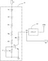
所述过压保护电路21包括第一瞬态抑制二极管T1、第二瞬态抑制二极管T2、第一电阻R1、第二电阻R2、第三电阻R3、第四电阻R4、第五电阻R5、电容C、三极管Q;
The
所述第一瞬态抑制二极管T1的阴极接第一电压V1、阳极与所述第二瞬态抑制二极管T2的阴极连接,所述第二瞬态抑制二极管T2的阳极依次经过第一电阻R1、第二电阻R2、第三电阻R3与所述第四电阻R4的第一端连接,所述电容C两端分别与所述第四电阻R4的两端连接,所述三极管Q为NPN型三极管,所述三极管Q的发射极与所述第四电阻R4的第二端连接后接地,所述三极管Q的集电极经第五电阻R5与所述待机芯片141的反馈端FB连接。
The cathode of the first transient suppression diode T1 is connected to the first voltage V1, and the anode is connected to the cathode of the second transient suppression diode T2, and the anode of the second transient suppression diode T2 passes through the first resistor R1, The second resistor R2 and the third resistor R3 are connected to the first end of the fourth resistor R4, the two ends of the capacitor C are respectively connected to the two ends of the fourth resistor R4, the transistor Q is an NPN transistor, The emitter of the transistor Q is connected to the second end of the fourth resistor R4 and grounded, and the collector of the transistor Q is connected to the feedback terminal FB of the
本实用新型的另一目的在于提供一种电视机,包括上述电源电路。 Another object of the present utility model is to provide a TV set, including the above-mentioned power supply circuit. the
阐述工作原理如下: The working principle is explained as follows:
图1所示电源电路为32寸以上液晶通用电源的电源结构框图。交流电经过整流滤波电路11后送到功率因数校正升压电路12,然后让大电解电容滤波电路13将波形虑平滑,平滑后的直流电一路提供给待机DC/DC电源电路14(提供5V),另一路提供给主功率DC/DC电源电路15(提供24V和12V),功率因数校正升压电路12和主功率DC/DC电源电路15的控制芯片都由待机DC/DC电源电路14提供,只有待机DC/DC电源电路14工作正常后,功率因数校正升压电路12和主功率DC/DC电源电路15才开始正常工作。
The power supply circuit shown in Figure 1 is a block diagram of the power supply structure of the LCD universal power supply above 32 inches. The alternating current is sent to the power factor
图2所示的电源电路是增加了过压保护电路21的电路框图,过压保护电路21采样大电解电容上的直流电压,当电压升高到一定幅值时,过压保护电路21给待机DC/DC电源电路14提供一个关机信号把功率因数校正升压电路12的供电关断,从而抑制电解电容上电压的上升。
The power supply circuit shown in Figure 2 is a circuit block diagram with an
如图3所示,电源电路在正常工作状态下,第一电压V1处于正常压值范围之内,经第一瞬态抑制二极管T1和第二瞬态抑制二极管T2的钳位作用,电压降为0V,三极管Q不导通,对待机芯片141的反馈端FB没有影响,待机芯片141正常工作。
As shown in Figure 3, when the power supply circuit is in a normal working state, the first voltage V1 is within the normal voltage range, and the voltage drop is 0V, the transistor Q is not conducting, which has no effect on the feedback terminal FB of the
当功率因数校正升压电路12输出的第一电压V1异常升高时,经第一瞬态抑制二极管T1和第二瞬态抑制二极管T2的钳位作用,电压依旧为高电平,经过第一电阻R1、第二电阻R2、第三电阻R3、第四电阻R4、电容C的分压滤波之后,所述三极管Q的基极为高电平,三极管Q导通,所述待机芯片141的反馈端FB经过第五电阻R5接地,反馈端FB降为低电平,待机芯片141停止工作,所述待机DC/DC电源电路14停止为功率因数校正升压电路12供电,从而避免了功率因数校正电路工作出现异常时发生电解电容爆裂等严重后果。
When the first voltage V1 output by the power factor
本新型提供的电源电路,能够有效防止功率因数校正电路工作出现异常时发生电解电容爆裂等严重后果,同时对后级电路也起到了一定的保护作用。由于过压保护电路所采用的元件都是成本比较低的电阻、电容、三极管等,所以在成本上也不会增加很多,为电源技术的应用与发展提供了一条新的思路和方法。 The power supply circuit provided by the utility model can effectively prevent serious consequences such as bursting of electrolytic capacitors when the power factor correction circuit works abnormally, and at the same time, it also has a certain protective effect on the subsequent stage circuit. Since the components used in the overvoltage protection circuit are relatively low-cost resistors, capacitors, triodes, etc., the cost will not increase a lot, which provides a new idea and method for the application and development of power supply technology. the
以上所述仅为本实用新型的较佳实施例而已,并不用以限制本实用新型,凡在本实用新型的精神和原则之内所作的任何修改、等同替换和改进等,均应包含在本实用新型的保护范围之内。 The above descriptions are only preferred embodiments of the present utility model, and are not intended to limit the present utility model. Any modifications, equivalent replacements and improvements made within the spirit and principles of the present utility model shall be included in this utility model. within the scope of protection of utility models. the
Claims (4)
Priority Applications (1)
| Application Number | Priority Date | Filing Date | Title |
|---|---|---|---|
| CN2012200963000U CN202495873U (en) | 2012-03-15 | 2012-03-15 | Power supply circuit and television |
Applications Claiming Priority (1)
| Application Number | Priority Date | Filing Date | Title |
|---|---|---|---|
| CN2012200963000U CN202495873U (en) | 2012-03-15 | 2012-03-15 | Power supply circuit and television |
Publications (1)
| Publication Number | Publication Date |
|---|---|
| CN202495873U true CN202495873U (en) | 2012-10-17 |
Family
ID=47002085
Family Applications (1)
| Application Number | Title | Priority Date | Filing Date |
|---|---|---|---|
| CN2012200963000U Expired - Lifetime CN202495873U (en) | 2012-03-15 | 2012-03-15 | Power supply circuit and television |
Country Status (1)
| Country | Link |
|---|---|
| CN (1) | CN202495873U (en) |
Cited By (1)
| Publication number | Priority date | Publication date | Assignee | Title |
|---|---|---|---|---|
| CN110461072A (en) * | 2019-07-22 | 2019-11-15 | 深圳市海洋王照明工程有限公司 | A kind of isolation light adjusting circuit and a kind of lamps and lanterns |
-
2012
- 2012-03-15 CN CN2012200963000U patent/CN202495873U/en not_active Expired - Lifetime
Cited By (2)
| Publication number | Priority date | Publication date | Assignee | Title |
|---|---|---|---|---|
| CN110461072A (en) * | 2019-07-22 | 2019-11-15 | 深圳市海洋王照明工程有限公司 | A kind of isolation light adjusting circuit and a kind of lamps and lanterns |
| CN110461072B (en) * | 2019-07-22 | 2021-09-03 | 深圳市海洋王电网照明技术有限公司 | Isolation dimming circuit and lamp |
Similar Documents
| Publication | Publication Date | Title |
|---|---|---|
| CN107681636A (en) | A kind of overvoltage crowbar and Switching Power Supply | |
| CN204258271U (en) | A kind of under-voltage protective switch of the short circuit supply unit | |
| CN207504562U (en) | A kind of protection circuit against input over-voltage for having the function of to power on Inrush current restraining | |
| TW201351865A (en) | Voltage conversion circuit | |
| CN204068199U (en) | A kind of under-voltage surge current protection circuit | |
| CN203491680U (en) | Automatic reset electric leakage overvoltage/undervoltage protection circuit | |
| CN202495873U (en) | Power supply circuit and television | |
| CN113964808B (en) | Hot plug line input end spike suppression device | |
| CN101267111B (en) | DC over-voltage protection circuit | |
| CN102403697B (en) | A kind of Switching Power Supply over-voltage over-current protection circuit and guard method | |
| CN106207959A (en) | Electromagnetism voltage-stabilizing energy-saving device over-voltage over-current protection device | |
| CN205427758U (en) | Computer hardware protection circuit | |
| CN203617678U (en) | Power supply system used for automatic reclosing breaker | |
| CN201418030Y (en) | Power supply with surge current prevention | |
| CN204103467U (en) | A kind of protective circuit of automobile instrument circuit | |
| WO2020073418A1 (en) | Input overvoltage protection circuit and power source system | |
| CN109066636A (en) | A kind of circuit of Anti-surging | |
| CN204668922U (en) | A kind of module power supply short-circuit protective circuit | |
| CN204794678U (en) | Outage self discharge control circuit | |
| CN205489479U (en) | Low -cost safety protection power | |
| CN205544913U (en) | Anti -interference steady voltage DC power supply controller | |
| CN206977324U (en) | Power circuit for low-voltage circuit breaker | |
| CN201408984Y (en) | A power supply protection circuit, a power supply device and a television set | |
| CN2935667Y (en) | Output overvoltage protection circuit of PFC circuit and TV set equipped with the circuit | |
| CN223451824U (en) | A switching power supply with high efficiency surge protection |
Legal Events
| Date | Code | Title | Description |
|---|---|---|---|
| C14 | Grant of patent or utility model | ||
| GR01 | Patent grant | ||
| CX01 | Expiry of patent term | ||
| CX01 | Expiry of patent term |
Granted publication date: 20121017 |