CN202353452U - Passive discharge circuit at input terminal of inverter - Google Patents
Passive discharge circuit at input terminal of inverter Download PDFInfo
- Publication number
- CN202353452U CN202353452U CN2011204824553U CN201120482455U CN202353452U CN 202353452 U CN202353452 U CN 202353452U CN 2011204824553 U CN2011204824553 U CN 2011204824553U CN 201120482455 U CN201120482455 U CN 201120482455U CN 202353452 U CN202353452 U CN 202353452U
- Authority
- CN
- China
- Prior art keywords
- resistance
- inverter
- discharge circuit
- connects
- input
- Prior art date
- Legal status (The legal status is an assumption and is not a legal conclusion. Google has not performed a legal analysis and makes no representation as to the accuracy of the status listed.)
- Withdrawn - After Issue
Links
Images


Classifications
-
- H—ELECTRICITY
- H03—ELECTRONIC CIRCUITRY
- H03K—PULSE TECHNIQUE
- H03K2217/00—Indexing scheme related to electronic switching or gating, i.e. not by contact-making or -breaking covered by H03K17/00
- H03K2217/0081—Power supply means, e.g. to the switch driver
Abstract
The utility model discloses a passive discharge circuit at the input terminal of an inverter. The passive discharge circuit comprises a first branch circuit connected in parallel with a DC-side capacitor, a second branch circuit connected in parallel with the DC-side capacitor, a comparator, an AND unit and a transistor driving circuit, wherein the first branch circuit consists of a discharge resistor and a switching transistor which are connected in series; the second branch circuit consists of a plurality of resistors connected in series; one input terminal of the comparator is connected with a triangular wave generator, and another input terminal of the comparator is connected between any two resistors in the second branch circuit; an enabling signal of the inverter is accessed into one input terminal of the AND unit, and another input terminal of the AND unit is connected with the output terminal of the comparator; and the input terminal of the transistor driving circuit is connected with the output terminal of the AND unit, and the output terminal of the transistor driving circuit controls the on/off of the switching transistor through a switching resistor. The passive discharge circuit adopts an adjustable conductive discharge circuit, is simple in design and control, improves the integral efficiency and shortens the discharge time, thereby avoiding conflict between the efficiency and the discharge time.
Description
Technical field
The utility model relates to and a kind of direct current is transformed into the inverter (Inverter) of alternating current, especially relates to a kind of automobile-used inverter that is used for electric automobile (EV) and hybrid vehicle (HEV).
Background technology
See also Fig. 1, automobile-used inverter adopts typical three-phase full-bridge voltage source type inverter usually, and it is made up of six transistor Q1~Q6, output three-phase alternating current u, v, w.Dc bus capacitor wherein (DC link capacitor) is as the load balance energy-storage travelling wave tube between DC side (batteries) and the AC side (alternating current machine).
The inverter input terminal voltage that in electric automobile and hybrid vehicle, uses is higher than 100V, is the protection personal safety, requires to be furnished with discharge circuit at the dc bus capacitor of inverter, to reduce the voltage of dc bus capacitor.Discharge circuit at the inverter input comprises two kinds: a kind of is passive discharge circuit, and GB GB18488 requires it in 120 seconds, to drop to below 60 volts through the voltage of passive discharge with dc bus capacitor; Another kind is the active discharge circuit, and it dropped to standard-required below 60 volts through the voltage of active discharge with dc bus capacitor in 5 seconds.
The active discharge circuit of existing inverter input is DC-to-dc converter (DC-DCConverter), and its two inputs are identical with two inputs of inverter.But DC-to-dc converter needs certain input voltage ability operate as normal, just will change circuit structure and control strategy for satisfying standard-required, has increased design difficulty and cost.
A kind of passive discharge circuit of existing inverter input is exactly at passive discharge resistance of the two ends of dc bus capacitor parallel connection, to realize passive discharge.Simplicity of design, the cost of this passive discharge circuit is low, scheme is ripe.But the loss that passive discharge resistance produced and the velocity of discharge are a pair of contradiction.For satisfying standard, must choose the passive discharge resistance of less resistance, 100K ohm for example, this can cause the whole efficiency of inverter on average to lose 0.1% approximately.
The another kind of passive discharge circuit of existing inverter input is main circuit and the driver that passive discharge resistance is placed converter main circuit and driver or DC-to-dc converter; This way can be saved volume; Reduce local pyrexia, but still can't solve the contradiction of efficient and discharge time.
The utility model content
The utility model technical problem to be solved provides a kind of passive discharge circuit of inverter input, is satisfying the operating efficiency that has improved inverter under the prerequisite of standard code.
The passive discharge circuit of the utility model inverter input comprises:
First branch road parallelly connected with dc bus capacitor, this first route discharge resistance and switching transistor are composed in series;
Second branch road parallelly connected with dc bus capacitor, these second a plurality of resistance of route is composed in series;
A comparator, an one of which input connects a triangular-wave generator, and another input connects between any two resistance in second branch road;
One and door, an one of which input inserts the enable signal of inverter, and another input connects the output of comparator;
Transistor driver circuit, its input connects the output with door, and its output is through a transistorized conducting of switch resistance control switch or end.
Further, said passive discharge circuit also comprises power supply circuits, and these power supply circuits comprise a three terminal regulator, and its three ports are negative electrode, anode and reference edge; Its negative electrode is exported the 12V power supply, and connects the positive pole of dc bus capacitors through one or more series resistances; Its plus earth; Its reference edge connects its negative electrode through a resistance, connects its anode through another resistance again.
Further, the resistance of said discharge resistance is 10~50k Ω.
Further, an input of said comparator obtains triangular signal, and another input obtains dc voltage value Vdc, and the amplitude of triangular signal is greater than dc voltage value Vdc; Pulse-modulated signal of comparator output.
Further, during the inverter operate as normal, the enable signal of its output is a high level, otherwise the enable signal of its output is a low level; And the enable signal of inverter is earlier through a non-input that inserts again behind the door with door.
Further, said switching transistor is that bipolar transistor is a triode; Discharge resistance connects the collector electrode of triode and the positive pole of dc bus capacitor, and the emitter of triode links to each other with the negative pole of dc bus capacitor; The output of transistor driver circuit connects the base stage of triode.
Further, said switching transistor is a field-effect transistor; Discharge resistance connects the collector electrode of field-effect transistor and the positive pole of dc bus capacitor, and the emitter of field-effect transistor links to each other with the negative pole of dc bus capacitor; The output of transistor driver circuit connects the grid of field-effect transistor.
Further, the output of said transistor driver circuit is identical with input.
Further, the resistance of connecting of the one or more resistance between the positive pole of the junction of comparator input and second branch road and dc bus capacitor is greater than 500k Ω.
Further, the resistance of connecting of the one or more resistance between the positive pole of the negative electrode of said three terminal regulator and dc bus capacitor is greater than 500k Ω; And the negative electrode of this three terminal regulator and the resistance of the resistance between the reference edge are four times of resistance of the resistance between anode and the reference edge.
The utility model adopts a kind of adjustable conductive discharge circuit; Design and control are simple, improve whole efficiency, and have shortened discharge time; Thereby solved the contradiction of efficient and discharge time; And the utility model can improve the discharge capability of passive discharge circuit, as replenishing of active discharge circuit.
Description of drawings
Fig. 1 is the sketch map of typical three-phase full-bridge voltage source type inverter;
Fig. 2 is the sketch map of the passive discharge circuit of the utility model inverter input;
Fig. 3 is the sketch map of the 12V power supply circuits that design of the utility model.
Description of reference numerals among the figure:
11 is triangular-wave generator; 12 is comparator; 13 are and door; 14 is transistor driver circuit; 15 is pressurizer.
Embodiment
See also Fig. 2, this is the sketch map of the passive discharge circuit of the utility model inverter input.This passive discharge circuit comprises:
First branch road parallelly connected with dc bus capacitor, this first route discharge resistance Rdis and switching transistor Q7 are composed in series.The resistance of said discharge resistance Rdis can be taken all factors into consideration factors such as discharge capability, power consumption, volume, 10~50k Ω (kilo-ohm) scope in choose.
Second branch road parallelly connected with dc bus capacitor, these second a plurality of resistance of route is composed in series, and is schematically illustrated as resistance R 1~R6 series connection among Fig. 1.
A comparator (Comparator) 12; An one of which input connects a triangular-wave generator (Triangle Wave Generator) 11 and obtains triangular signal; Another input connects between any two resistance in second branch road; For example be between resistance R 5 and the R6, to obtain dc voltage value Vdc.The amplitude of said triangular signal is greater than dc voltage value Vdc.Comparator 12 realizes to its output being the duty ratio control of pwm signal through comparing dc voltage value Vdc and triangular signal.
One and door (AND) 13, an one of which input inserts the enable signal Enable of inverter, and another input connects the output of comparator 12.Preferably, during the inverter operate as normal, the enable signal Enable of its output is a high level, otherwise the enable signal Enable of its output is a low level.And the enable signal Enable of inverter is earlier through inserting an input with door 13 after the not gate anti-phase again, and is as shown in Figure 2.
Transistor driver circuit (MosFET Driver) 14, its input connects the output with door 13, its output through a switch resistance Rg control switch transistor Q1 conducting or end.Switch resistance Rg generally gets 10~15 Ω, realizes the normal switch of switching transistor Q7.
T+ among the figure, T-represent anode, the negative terminal of dc bus capacitor respectively.
Said switching transistor Q1 can be bipolar transistor (being triode).Discharge resistance Rdis connects the collector electrode of triode Q1 and the positive pole of dc bus capacitor, and the emitter of triode Q1 links to each other with the negative pole of dc bus capacitor.The output of transistor driver circuit 14 connects the base stage of triode Q1.
Said switching transistor Q1 also can be a field-effect transistor.Discharge resistance Rdis connects the collector electrode of field-effect transistor Q1 and the positive pole of dc bus capacitor, and the emitter of field-effect transistor Q1 links to each other with the negative pole of dc bus capacitor.The output of transistor driver circuit 14 connects the grid of field-effect transistor Q1.
The output of said transistor driver circuit 14 is identical with input, promptly input be low level then output also for low level, input be high level then output also be high level.It mainly plays a part power amplification.
Because an input of comparator 12 is connected between any two resistance of second branch road, a plurality of series resistances of second branch road have just been formed a bleeder circuit so.Wherein, the resistance of connecting of the one or more resistance between the positive pole of this input of comparator 12 and dc bus capacitor is preferably greater than 500k Ω, to realize the high-low pressure insulation function.
The operation principle of the passive discharge circuit of the utility model inverter input is described below:
When the inverter operate as normal, the enable signal Enable that inverter provides is a high level.With the output of door 13 be low level, the input signal IN of transistor driver circuit 14 and output signal OUT are low level, switching transistor Q7 is normally closed, discharge circuit is not worked and is not produced loss yet.
When inverter standby or outage, the enable signal Enable that inverter provides is a low level.An input of comparator 12 obtains dc voltage value Vdc from second branch road; Comparator 12 relatively obtains a PWM (pulse-width modulation) signal with the triangular signal of this dc voltage value Vdc and triangular-wave generator 11 generations; Be this pwm signal with the input of door 13; The input signal IN of transistor driver circuit 14 and output signal OUT are this pwm signal, switching transistor Q7 intermittent conducting and ending under the control of this pwm signal.When switching transistor Q1 conducting, realize passive discharge.
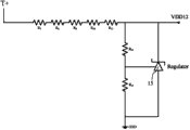
In the passive discharge circuit of the utility model inverter input, triangular-wave generator 11, comparator 12, need use power supply with door 13, transistor driver circuit 14.Guarantee that when low-tension supply 12V cuts off the power supply passive discharge circuit still can operate as normal, so also comprises power supply circuits in the utility model alternatively, and is as shown in Figure 3.The power taking from the positive pole of dc bus capacitor of these power supply circuits uses pressurizer (Regulator) to produce 12V power supply VDD12.When the inverter operate as normal, the passive discharge circuit of the utility model is not worked, and its loss approximates zero, so this power supply circuits loss also approximates zero.
See also Fig. 3, the negative electrode of said three terminal regulator 15 (CATHODE) is exported 12V power supply VDD12, and connects the positive pole of dc bus capacitors through one or more series resistances.Fig. 3 schematically shows out its negative electrode connects dc bus capacitor through the resistance R 7~R11 of series connection positive pole.Its anode (ANODE) ground connection.Its reference edge (REF) connects its negative electrode through resistance R 12 on the one hand, connects its anode through resistance R 13 on the other hand.
Preferably, the resistance of connecting of the one or more resistance between the negative electrode of this three terminal regulator 15 and the positive pole of dc bus capacitor is greater than 500K ohm, to realize the high-low pressure insulation function.And the negative electrode of this three terminal regulator 15 and the resistance of the resistance R between the reference edge 12 are four times of resistance of the resistance R 13 between anode and the reference edge, guarantee its output 12V power supply.
The utility model adopts pulse signal control switch transistor, and when can be implemented in the inverter operate as normal, passive discharge circuit is not worked, thereby has improved system effectiveness.
The utility model is realized the adjustable ground discharge through the duty ratio of control wave; Can realize the passive discharge of obstructed speed to obstructed dc capacitor voltage; Make full use of the 120 second time of stipulating in the safety standard, reduce the discharge resistance heating, increase the life-span.
The utility model can improve passive discharge capability, as replenishing of active discharge circuit.Have at the same time in the inverter of active discharge circuit, the described passive discharge circuit of the utility model can help DC-to-dc converter to accomplish the demand of initiatively discharging under lower dc capacitor voltage.
More than be merely the preferred embodiment of the utility model, and be not used in qualification the utility model.For a person skilled in the art, the utility model can have various changes and variation.All within the spirit and principle of the utility model, any modification of being done, be equal to replacement, improvement etc., all should be included within the protection range of the utility model.
Claims (10)
1. the passive discharge circuit of an inverter input is characterized in that, comprising:
First branch road parallelly connected with dc bus capacitor, this first route discharge resistance and switching transistor are composed in series;
Second branch road parallelly connected with dc bus capacitor, these second a plurality of resistance of route is composed in series;
A comparator, an one of which input connects a triangular-wave generator, and another input connects between any two resistance in second branch road;
One and door, an one of which input inserts the enable signal of inverter, and another input connects the output of comparator;
Transistor driver circuit, its input connects the output with door, and its output is through a transistorized conducting of switch resistance control switch or end.
2. the passive discharge circuit of inverter input according to claim 1 is characterized in that, said passive discharge circuit also comprises power supply circuits, and these power supply circuits comprise a three terminal regulator, and its three ports are negative electrode, anode and reference edge; Its negative electrode is exported the 12V power supply, and connects the positive pole of dc bus capacitors through one or more series resistances; Its plus earth; Its reference edge connects its negative electrode through a resistance, connects its anode through another resistance again.
3. the passive discharge circuit of inverter input according to claim 1 is characterized in that, the resistance of said discharge resistance is 10~50k Ω.
4. the passive discharge circuit of inverter input according to claim 1; It is characterized in that; An input of said comparator obtains triangular signal, and another input obtains dc voltage value Vdc, and the amplitude of triangular signal is greater than dc voltage value Vdc; Pulse-modulated signal of comparator output.
5. the passive discharge circuit of inverter input according to claim 1 is characterized in that, during the inverter operate as normal, the enable signal of its output is a high level, otherwise the enable signal of its output is a low level; And the enable signal of inverter is earlier through a non-input that inserts again behind the door with door.
6. the passive discharge circuit of inverter input according to claim 1 is characterized in that, said switching transistor is that bipolar transistor is a triode; Discharge resistance connects the collector electrode of triode and the positive pole of dc bus capacitor, and the emitter of triode links to each other with the negative pole of dc bus capacitor; The output of transistor driver circuit connects the base stage of triode.
7. the passive discharge circuit of inverter input according to claim 1 is characterized in that said switching transistor is a field-effect transistor; Discharge resistance connects the collector electrode of field-effect transistor and the positive pole of dc bus capacitor, and the emitter of field-effect transistor links to each other with the negative pole of dc bus capacitor; The output of transistor driver circuit connects the grid of field-effect transistor.
8. the passive discharge circuit of inverter input according to claim 1 is characterized in that, the output of said transistor driver circuit is identical with input.
9. the passive discharge circuit of inverter input according to claim 1 is characterized in that, the resistance of connecting of the one or more resistance between the positive pole of input of comparator and the junction of second branch road and dc bus capacitor is greater than 500k Ω.
10. the passive discharge circuit of inverter input according to claim 1 is characterized in that, the resistance of connecting of the one or more resistance between the negative electrode of said three terminal regulator and the positive pole of dc bus capacitor is greater than 500k Ω; And the negative electrode of this three terminal regulator and the resistance of the resistance between the reference edge are four times of resistance of the resistance between anode and the reference edge.
Priority Applications (1)
| Application Number | Priority Date | Filing Date | Title |
|---|---|---|---|
| CN2011204824553U CN202353452U (en) | 2011-11-28 | 2011-11-28 | Passive discharge circuit at input terminal of inverter |
Applications Claiming Priority (1)
| Application Number | Priority Date | Filing Date | Title |
|---|---|---|---|
| CN2011204824553U CN202353452U (en) | 2011-11-28 | 2011-11-28 | Passive discharge circuit at input terminal of inverter |
Publications (1)
| Publication Number | Publication Date |
|---|---|
| CN202353452U true CN202353452U (en) | 2012-07-25 |
Family
ID=46542414
Family Applications (1)
| Application Number | Title | Priority Date | Filing Date |
|---|---|---|---|
| CN2011204824553U Withdrawn - After Issue CN202353452U (en) | 2011-11-28 | 2011-11-28 | Passive discharge circuit at input terminal of inverter |
Country Status (1)
| Country | Link |
|---|---|
| CN (1) | CN202353452U (en) |
Cited By (5)
| Publication number | Priority date | Publication date | Assignee | Title |
|---|---|---|---|---|
| CN102437771A (en) * | 2011-11-28 | 2012-05-02 | 联合汽车电子有限公司 | Passive discharging circuit of inverter input terminal |
| CN107437793A (en) * | 2017-09-07 | 2017-12-05 | 艾思玛新能源技术(扬中)有限公司 | A kind of floating pressure process circuit of multichannel MPPT photovoltaic DC-to-AC converters |
| CN112693315A (en) * | 2020-12-01 | 2021-04-23 | 广州橙行智动汽车科技有限公司 | Vehicle discharge circuit, method, device, vehicle and storage medium |
| WO2022262893A1 (en) * | 2021-06-15 | 2022-12-22 | Schaeffler Technologies AG & Co. KG | Active discharge of a vehicle intermediate circuit element using a discrete pwm pulse-generating discharge circuit |
| CN116780879A (en) * | 2023-08-23 | 2023-09-19 | 浙江奥思伟尔电动科技有限公司 | Active discharging circuit of high-voltage driving controller of electric automobile, controller and automobile |
-
2011
- 2011-11-28 CN CN2011204824553U patent/CN202353452U/en not_active Withdrawn - After Issue
Cited By (6)
| Publication number | Priority date | Publication date | Assignee | Title |
|---|---|---|---|---|
| CN102437771A (en) * | 2011-11-28 | 2012-05-02 | 联合汽车电子有限公司 | Passive discharging circuit of inverter input terminal |
| CN107437793A (en) * | 2017-09-07 | 2017-12-05 | 艾思玛新能源技术(扬中)有限公司 | A kind of floating pressure process circuit of multichannel MPPT photovoltaic DC-to-AC converters |
| CN112693315A (en) * | 2020-12-01 | 2021-04-23 | 广州橙行智动汽车科技有限公司 | Vehicle discharge circuit, method, device, vehicle and storage medium |
| WO2022262893A1 (en) * | 2021-06-15 | 2022-12-22 | Schaeffler Technologies AG & Co. KG | Active discharge of a vehicle intermediate circuit element using a discrete pwm pulse-generating discharge circuit |
| CN116780879A (en) * | 2023-08-23 | 2023-09-19 | 浙江奥思伟尔电动科技有限公司 | Active discharging circuit of high-voltage driving controller of electric automobile, controller and automobile |
| CN116780879B (en) * | 2023-08-23 | 2023-11-24 | 浙江奥思伟尔电动科技有限公司 | Active discharging circuit of high-voltage driving controller of electric automobile, controller and automobile |
Similar Documents
| Publication | Publication Date | Title |
|---|---|---|
| CN102437771A (en) | Passive discharging circuit of inverter input terminal | |
| US9931944B2 (en) | Variable voltage convert system with reduced bypass diode conduction | |
| CN102299655B (en) | Drive electric device and the correlation technique of plant equipment | |
| US7728562B2 (en) | Voltage link control of a DC-AC boost converter system | |
| CN108306488B (en) | Variable voltage converter for obtaining lower minimum step-up ratio | |
| US10574144B1 (en) | System and method for a magnetically coupled inductor boost and multiphase buck converter with split duty cycle | |
| D'arco et al. | A modular converter with embedded battery cell balancing for electric vehicles | |
| CN202353452U (en) | Passive discharge circuit at input terminal of inverter | |
| US9592746B2 (en) | Power net system of fuel cell hybrid vehicle and charge/discharge control method | |
| US10790763B2 (en) | HEV e-drives with HV boost ratio and wide DC bus voltage range | |
| CN102969918B (en) | Three-phase bridge type converter system and promptly descend short-circuit protection circuit | |
| CN103227610A (en) | Motor control circuit and automobile | |
| CN107306077B (en) | IGBT gate drive during turn-off to reduce switching losses | |
| EP4258539A3 (en) | Multilevel motor drive with integrated battery charger | |
| CN109687559A (en) | A kind of electricity of power battery-electricity mixed power supply system | |
| CN103730940A (en) | Vehicle-mounted charger of electric automobile | |
| DE102019116823A1 (en) | HYBRID VEHICLE DRIVETRAIN WITH INSULATED DOUBLE BUS | |
| CN103296900A (en) | Direct voltage capture device for energy storage device and method for generating direct voltage by energy storage device | |
| EP2717417A1 (en) | Battery system | |
| Tan et al. | Effective voltage balance control for three-level bidirectional dc-dc converter based electric vehicle fast charger | |
| US10389352B1 (en) | Gate loop differential mode choke for parallel power device switching current balance | |
| Salari et al. | A new multiple input bidirectional HEV battery charger | |
| CN111740584A (en) | Single-phase staggered and three-phase Vienna topology compatible input PFC device | |
| Bubovich | Use of Multilevel Converters in Light Vehicles of Orthopedic Rehabilitation | |
| CN220809144U (en) | Charging system and electric automobile |
Legal Events
| Date | Code | Title | Description |
|---|---|---|---|
| C14 | Grant of patent or utility model | ||
| GR01 | Patent grant | ||
| AV01 | Patent right actively abandoned |
Granted publication date: 20120725 Effective date of abandoning: 20191220 |
|
| AV01 | Patent right actively abandoned |
Granted publication date: 20120725 Effective date of abandoning: 20191220 |
|
| AV01 | Patent right actively abandoned | ||
| AV01 | Patent right actively abandoned |