CN1959922A - Image display device - Google Patents
Image display device Download PDFInfo
- Publication number
- CN1959922A CN1959922A CNA2006101427283A CN200610142728A CN1959922A CN 1959922 A CN1959922 A CN 1959922A CN A2006101427283 A CNA2006101427283 A CN A2006101427283A CN 200610142728 A CN200610142728 A CN 200610142728A CN 1959922 A CN1959922 A CN 1959922A
- Authority
- CN
- China
- Prior art keywords
- mentioned
- wiring
- display device
- image display
- sealing area
- Prior art date
- Legal status (The legal status is an assumption and is not a legal conclusion. Google has not performed a legal analysis and makes no representation as to the accuracy of the status listed.)
- Pending
Links
Images


Classifications
-
- H—ELECTRICITY
- H01—ELECTRIC ELEMENTS
- H01J—ELECTRIC DISCHARGE TUBES OR DISCHARGE LAMPS
- H01J29/00—Details of cathode-ray tubes or of electron-beam tubes of the types covered by group H01J31/00
- H01J29/90—Leading-in arrangements; Seals therefor
-
- H—ELECTRICITY
- H01—ELECTRIC ELEMENTS
- H01J—ELECTRIC DISCHARGE TUBES OR DISCHARGE LAMPS
- H01J29/00—Details of cathode-ray tubes or of electron-beam tubes of the types covered by group H01J31/00
- H01J29/86—Vessels; Containers; Vacuum locks
- H01J29/87—Arrangements for preventing or limiting effects of implosion of vessels or containers
-
- H—ELECTRICITY
- H01—ELECTRIC ELEMENTS
- H01J—ELECTRIC DISCHARGE TUBES OR DISCHARGE LAMPS
- H01J31/00—Cathode ray tubes; Electron beam tubes
- H01J31/08—Cathode ray tubes; Electron beam tubes having a screen on or from which an image or pattern is formed, picked up, converted, or stored
- H01J31/10—Image or pattern display tubes, i.e. having electrical input and optical output; Flying-spot tubes for scanning purposes
- H01J31/12—Image or pattern display tubes, i.e. having electrical input and optical output; Flying-spot tubes for scanning purposes with luminescent screen
- H01J31/123—Flat display tubes
- H01J31/125—Flat display tubes provided with control means permitting the electron beam to reach selected parts of the screen, e.g. digital selection
- H01J31/127—Flat display tubes provided with control means permitting the electron beam to reach selected parts of the screen, e.g. digital selection using large area or array sources, i.e. essentially a source for each pixel group
Landscapes
- Cathode-Ray Tubes And Fluorescent Screens For Display (AREA)
- Electrodes For Cathode-Ray Tubes (AREA)
Abstract
An image display device is constituted such that a back substrate on which image signal lines, scanning signal lines and electron sources are arranged and a face substrate which has phosphor layers are hermetically sealed to each other by way of a frame body using a sealing material, and the inside of the image display device is formed into a vacuum. A length LSK of a second sealing region into which scanning signal lines hermetically penetrate is set larger than a length LDK of a first sealing region into which thin-film image signal lines hermetically penetrate and hence, it is possible to suppress the decrease of the degree of vacuum.
Description
Technical field
The present invention relates to utilize the flat-panel type picture display device of the electronics emission in the vacuum that is formed between front substrate and the back substrate.
Background technology
As at outstanding display device aspect high brightness, the high definition, be extensive use of color cathode ray tube in the past.But, be accompanied by the information processor in recent years and the high image qualityization of televising, the requirement that has high brightness, high definition characteristic and lightweight, saves the flat-panel type picture display device (flat-panel monitor FPD) in space is improved.
As its exemplary, liquid crystal indicator, plasma display system etc. just is practical.In addition, especially as the display unit that can realize high brightness, as having utilized, make every effort to realize being called as the display unit of electron emitting-type image display device or field emission formula image display device and having the practicability of the various flat displays such as OLED display of low power consumption feature from the Autoluminescence display unit of electron source to the electronics emission of vacuum.
In the Autoluminescence flat-panel monitor in flat-panel type picture display device, have as everyone knows electron source is configured to rectangular structure,, help the aforementioned electronic emission-type image display device of can be little integrated cold cathode as everyone knows as one.
In addition, in the Autoluminescence flat-panel monitor, its cold cathode uses thin film electron sources such as Spindt type, surface conductive type, carbon nano tube type, MIM (Metal-Insulator-Metal) type that is laminated with metal-insulator-metal type, MIS (Metal-Insulator-Semiconductor) type that is laminated with metal-insulator semiconductor or metal-insulator semiconductor-metal mold etc.
About the mim type electron source, for example patent documentation 1, patent documentation 2 disclosed inventions are arranged as everyone knows.In addition, about metal-insulator semiconductor type electron source the MOS type that proposes in the non-patent literature 1 is arranged as everyone knows; About metal-insulator semiconductor-metal mold electron source porous silicon (poroussilicon) type electron source that EL type electron source that HEED type electron source that non-patent literature 2 grades propose, non-patent literature 3 etc. propose, non-patent literature 4 etc. propose etc. is arranged as everyone knows.
Well-known electron emitting-type FPD is a kind of display panel, by constituting with lower member: the back substrate with above-mentioned electron source; Has a front substrate of anode that luminescent coating and being formed for makes the accelerating voltage of this luminescent coating of electron bombard of launching from electron source with above-mentioned back substrate is opposed; And be sealed to the supporting mass that the sealing frame of predetermined vacuum state constitutes by inner space in opposite directions with two substrates.This display panel assembling drive circuit is made its work.
Comprise back substrate in the image display device of electron emitting-type, this back substrate has: a plurality of the 1st wirings (for example, negative electrode wiring, picture signal connect up) of extending and being set up in parallel in the 2nd direction of intersecting with the 1st direction along the 1st direction; The dielectric film that covers the 1st wiring and form; A plurality of the 2nd wirings (for example, grid wiring, scanning signal lines) that above-mentioned the 2nd direction is extended and is set up in parallel in above-mentioned the 1st direction in this dielectric film upper edge; And near the electron source of cross part that is arranged at above-mentioned the 1st wiring and above-mentioned the 2nd wiring, this back substrate has the substrate that is formed by insulating material, is formed with above-mentioned wiring on this substrate.
Apply sweep signal with this structure successively to above-mentioned scanning signal lines.In addition, the electron source that is connected to scanning signal lines and picture signal wiring is set on this substrate.Each wiring is connected by current electrode with each electrode that constitutes electron source, and electric current is offered electron source.Have a front substrate with this back substrate is opposed, this front substrate has the luminescent coating and the anode of a plurality of colors on above-mentioned opposed inner surface.Front substrate is formed by the translucent material of being advisable with glass.And have following structure: the inward flange of fitting to two substrates inserts as supporting mass that seals frame and sealing, and makes the inner space that is formed by this back substrate, front substrate and supporting mass become vacuum.
Electron source is positioned at the cross part of the 1st wiring and the 2nd wiring as mentioned above, with the emission measure (switch that comprise emission) of the potential difference control between the 1st wiring and the 2nd wiring from the electronics of electron source.The high voltage that anode applied that the electronics of launching is positioned on the front substrate quickens, and the luminescent coating by having on the bombardment excitation front substrate sends and the corresponding coloured light of its characteristics of luminescence this luminescent coating.
Each electron source and corresponding luminescent coating be the component unit pixel in couples.Usually, the unit picture element with red (R), green (G), blue (B) three kinds of colors constitutes a pixel (colour element, pixel).And under the situation that is colour element, unit picture element is called as secondary image element (sub-pixel).
In aforesaid flat-panel type picture display device, generally by the viewing area internal fixation that is centered on by said frame between back substrate and the front substrate a plurality of intervals holding members (hereinafter referred to as distance piece) are being set, being cooperated with said frame in the interval between the above-mentioned two substrates keeps predetermined space.This distance piece generally is made of the plate body that insulating material such as glass or pottery form, and usually, is arranged on the position that does not hinder pixel operation every a plurality of pixels.
In addition, the framework that forms the sealing frame is fixed on the inward flange of back substrate and front substrate by encapsulants such as fused glass, and this fixed part is hermetically sealed becomes sealing area.The vacuum degree of the inside, viewing area that is formed by two substrates and framework is for example 10
-5~10
-7Torr.
Be formed on the 1st wiring and the sealing area of the 2nd wiring perforation between framework and substrate of back substrate, the top ends of the 1st wiring and the 2nd wiring has the 1st wiring leading-out terminal and the 2nd wiring leading-out terminal.
Usually, be to form the frame fixation of sealing frame at above-mentioned back substrate and front substrate with encapsulants such as fused glass.
Patent documentation 1: the spy opens flat 7-65710 communique
Patent documentation 2: the spy opens flat 10-153979 communique
Patent documentation 3: the spy opens flat 9-277586 communique
Non-patent literature 1:j.Vac.Sci.Technol.B11 (2) is (1993) p.429-432
Non-patent literature 2:high-efficiency-electro-emission device, Jpn.J.Appl.Phys.vol36, pL939
Non-patent literature 3:Electroluminescence, Applied Physics the 63rd volume, No. 6,592 pages
Non-patent literature 4: Applied Physics the 66th volume, No. 5,437 pages
Summary of the invention
The 1st wiring and the 2nd wiring are configured on the back substrate, and these wiring perforation back substrate surfaces are with the opposed zone of framework end face and be drawn out to the outside.Constitute sealing area at the such encapsulant of this area configurations fused glass.According to such structure, for obtaining the display image of desired brightness, need flow into the electric current of Duoing to scanning signal lines than the picture signal wiring, produce the problem that voltage drop takes place along the said scanning signals wiring immediately.
For above-mentioned voltage drop is reduced, the resistance of said scanning signals wiring is reduced.Scan signal electrode is made of the film of the such metal material of for example Al (aluminium), but for resistance is reduced, need make the thickness of the metallic film that constitutes above-mentioned wiring increase (thickening).But if increase thickness, it is big that the stress of above-mentioned wiring becomes, and has the problem that easily comes off from back substrate.This problem exists in the structure of above-mentioned patent documentation 1 equally.
In addition, different with value of current flowing in the picture signal wiring for making in scanning signal lines, thickness is also different.The thick film part is than the easier generation vacuum leak of film portion.The vacuum degree that causes the vacuum viewing area of vacuum leak descends, and has the reliability problems that diminishes image display device.
And the narrow more problem of following flowing of above-mentioned encapsulant and producing of the width of sealing area is few more, under the situation that vacuum leak does not take place, wishes that the width of sealing area is narrow.
The object of the present invention is to provide a kind of prevention at image display device sealing area generation vacuum leak, reliability high life length.
For achieving the above object, the present invention takes to make thickness with it the corresponding structure of the width of sealing area according to the wiring that connects the sealing zone.
Image display device of the present invention, comprise panel, described panel comprises back substrate, front substrate, framework and containment member, to carry out exhaust by the space that above-mentioned back substrate and above-mentioned front substrate and said frame surround, described back substrate, have along the 1st direction and extend and a plurality of the 1st connecting up that the 2nd direction of intersecting with the 1st direction is set up in parallel, cover the dielectric film that above-mentioned the 1st wiring forms, a plurality of the 2nd wirings of extending and being set up in parallel in above-mentioned the 1st direction along above-mentioned the 2nd direction, and the electron source that is connected to above-mentioned the 1st wiring and above-mentioned the 2nd wiring, described front substrate, have by from the excitation of above-mentioned electron source electrons emitted and the luminescent coating and the anode of luminous a plurality of colors, and it is opposed with predetermined space and above-mentioned back substrate, described framework, between above-mentioned back substrate and above-mentioned front substrate, center on the viewing area, keep above-mentioned predetermined interval, described containment member, gas-tight seal said frame end face and above-mentioned front substrate, and said frame end face and back substrate respectively.
Above-mentioned image display device also has the 1st sealing area that has disposed the containment member that extends along the 2nd direction in above-mentioned a plurality of the 1st wirings; With the 2nd sealing area that in above-mentioned a plurality of the 2nd wirings, has disposed the containment member that extends along the 1st direction; The 1st direction width of above-mentioned the 1st sealing area is different with the 2nd direction width of above-mentioned the 2nd sealing area.
To having image display device assembly drawing image signal drive circuit, scan signal drive circuit, other peripheral circuit of these structures, constitute self-luminous planar display device.
Adopt the present invention,, can stop the generation of vacuum leak, obtain reliability height, long image display device of life-span according to being the length that the wiring of writing thick-film line or film changes the wiring perforation direction of sealing area.
In addition, the amount of the encapsulant that control is used and suppress it to the flowing of the part that does not need containment member can improve operability and guarantee display quality.
In the part of the sealing area between framework and above-mentioned back substrate, the length that is present in the sealing area part in the above-mentioned plate is different with above-mentioned plate length outward.The regional side of being deflated of sealing area (inboard) is compared with atmospheric pressure one side (outside), the length that its wiring connects direction is long, can guarantee thus between terminal and the external circuit in conjunction with the space, and stop the generation of vacuum leak, thereby can access reliability height, long image display device of life-span.
Above-mentioned the 1st wiring is different with the 2nd wiring thickness that is routed in the above-mentioned sealing area, can select the size of sealing area according to the wiring thickness thus, and stops the generation of vacuum leak, thereby can access reliability height, long image display device of life-span.
At least one of above-mentioned the 1st wiring and the 2nd wiring is that the wiring portion that is disposed in above-mentioned intralamellar part and the sealing area is made lit-par-lit structure, can easily realize writing thick-film line thus, thereby can improve the electrical characteristics in the vacuum viewing area and obtain cheap image display device.
Above-mentioned lit-par-lit structure contains the combination of the different material of conductivity, can guarantee electrical characteristics and the prevention generation at the vacuum leak of sealing area thus, obtains reliability height, long image display device of life-span.
Above-mentioned the 1st wiring is picture signal wiring, can select the size of sealing area stop to be accompanied by the mobile of encapsulant to have problems according to the wiring thickness thus, can access guarantee electrical characteristics, reliability height, long image display device of life-span.
Above-mentioned the 2nd wiring is a scanning signal lines, and the thickness that connects up thus is bigger than the picture signal wiring, and its effect is remarkable, and can stop the generation at the vacuum leak of sealing area, obtains reliability height, long image display device of life-span.
Description of drawings
Figure 1A is a vertical view of observing image display device of the present invention from the front substrate-side, and Figure 1B is the side view of Figure 1A.
Fig. 2 is the diagrammatic top view along the A-A line among Figure 1B.
Fig. 3 is the schematic sectional view along the schematic sectional view of the back substrate of the B-B line among Fig. 2 and a part of front substrate corresponding with its back substrate.
Fig. 4 is the schematic sectional view along the schematic sectional view of the back substrate of the C-C line among Fig. 2 and a part of front substrate corresponding with its back substrate.
Fig. 5 is the schematic sectional view along the schematic sectional view of the back substrate of the D-D line among Fig. 2 and a part of front substrate corresponding with its back substrate.
Fig. 6 is the schematic sectional view corresponding with 4 of another embodiment of image display device of the present invention.
Fig. 7 is the schematic sectional view corresponding with 3 of another embodiment of image display device of the present invention.
Fig. 8 is the schematic sectional view corresponding with 3 of another embodiment of image display device of the present invention.
Fig. 9 is the schematic sectional view along the E-E line among Fig. 8.
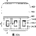
Figure 10 A-Figure 10 C is the accompanying drawing of an example of the electron source of the explanation pixel that constitutes image display device of the present invention.
Figure 11 is the key diagram of equivalent electric circuit example that is suitable for the image display device of structure of the present invention.
Embodiment
Below, with reference to the accompanying drawings embodiments of the present invention are elaborated.
[embodiment 1]
Fig. 1 to Fig. 5 is the accompanying drawing for the embodiment that image display device of the present invention is described, Figure 1A is the vertical view of observing from the front substrate-side, Figure 1B is the side view of Figure 1A, Fig. 2 is the diagrammatic top view along the A-A line among Figure 1B, Fig. 3 is the schematic sectional view along the schematic sectional view of the back substrate of the B-B line among Fig. 2 and a part of front substrate corresponding with its back substrate, Fig. 4 is the schematic sectional view along the schematic sectional view of the back substrate of the C-C line among Fig. 2 and a part of front substrate corresponding with its back substrate, and Fig. 5 is the schematic sectional view along the schematic sectional view of the back substrate of the D-D line among Fig. 2 and a part of front substrate corresponding with its back substrate.
In above-mentioned Fig. 1 to Fig. 5, Reference numeral 1 expression back substrate, 2 expression front substrates, this two substrates the 1, the 2nd, by thickness be several mm for example the glass plate about 1~10mm constitute, two substrates is shape in the form of a substantially rectangular all, and every stacked with predetermined space.
This framework 3 constitutes with identical pair of frames sheet 32 by combination pair of frames sheet 31, and pair of frames sheet 31 is configured in the long side of above-mentioned essentially rectangular shape, and pair of frames sheet 32 is configured in short brink.In addition, the thickness of these frame sheet 31,32, promptly the thickness T DK of frame sheet 31 is different with the thickness T SK of frame sheet 32.Framework 3 be inserted between the above-mentioned two substrates 1,2 edge part and with two substrates 1,2 airtight joints.On the other hand, it highly is configured to be substantially equal to the size at the above-mentioned interval between the two substrates 1,2.
Reference numeral 4 expression blast pipes, this blast pipe 4 is fixed on the above-mentioned back substrate 1.5 expression containment members, sealing member 5 is made of for example fused glass, and it engages said frame 3 and two substrates 1,2 and carries out gas-tight seal.
The space 6 that is surrounded by said frame 3, two substrates 1,2 and containment member 5 is by above-mentioned blast pipe 4 exhausts, for example keeps 10
-5~10
-7The vacuum degree of Torr.In addition, above-mentioned blast pipe 4 is installed in the outer surface of above-mentioned back substrate 1 as described above and is communicated to the through hole 7 that connects this back substrate 1 and run through setting, and after exhaust was finished, above-mentioned blast pipe 4 was sealed.
(Ts>Td) the above-mentioned other direction (directions X) of Xiang Yuqi intersection extends and is set up in parallel with an above-mentioned direction (Y direction) in above-mentioned picture signal wiring 8 and with thickness Ts for Reference numeral 9 expression scanning signal lines, this scanning signal lines 9.This scanning signal lines 9 connects framework 3 airtightly from viewing area 6 frame sheet 32 and the gas-tight seal portion between the back substrate 1 are that length is the 2nd sealing area 52 of LSK, extend to the outside of the short brink outer end of stacked above-mentioned front substrate 2 2b the end of the short brink of substrate 1 overleaf, and with its top ends as scanning signal lines leading-out terminal 91.
In addition, the pass of the length L DK of the perforation direction of the length L SK of the perforation direction of the 2nd sealing area 52 and above-mentioned the 1st sealing area 51 is LSK>LDK.
This LSK>LDK is that expression said scanning signals wiring 9 is as described above than the thickness of the above-mentioned picture signal wiring 8 (structure of Ts>Td).Consider this film thickness difference, the length L SK of perforation direction of the 2nd sealing area 52 that makes scanning signal lines 9 airtight perforations is than the connect up length L DK long (width is wide) of perforation direction of the 1st sealing area 51 of 8 airtight perforations of picture signal.
Here, for example Al (aluminium) film is used in above-mentioned picture signal wiring 8, and scanning signal lines 9 is used for example Cr/Al/Cr film, Cr/Cu/Cr film etc.In addition, above-mentioned wiring leading- out terminal 81,91 is set at the two ends of electrode, but also can only be arranged on any end.
Then, Reference numeral 12 expression distance pieces, this distance piece is made of ceramic material, and is shaped to rectangular thin sheet form, on every scanning signal lines 9,1 distance piece uprightly is set, it is connected and fixing with two substrates 1,2 with link 13 with said frame 3 almost parallel ground.This distance piece 12 can only at one end carry out with being connected and fixed of substrate, and its configuration is arranged on the position that does not hinder pixel operation every a plurality of pixels usually.
The size of this distance piece 12 is set according to the height of basic size, supporting mass 3, the material of substrate, the configuration space of distance piece, the material of distance piece etc., but usually its height is roughly the same with above-mentioned supporting mass 3, thickness smaller or equal to tens μ m to several mm, length is about 20mm to 1000mm, is practical value about preferred 80mm to 120mm.In addition, this distance piece 12 has 10
8~10
9Resistance about Ω cm.
Inner surface at the front substrate 2 of fixing these distance piece 12 1 ends is provided with redness, green, blue with luminescent coating 15, and divides with BM (black matrix) film 16 with shading.In order to cover them, the back of the body gold (anode electrode) 17 with for example vapour deposition method setting is made of metallic film forms the face.
As above-mentioned fluorophor, for example can use Y as redness
2O
2S:Eu (P22-R); Can use ZnS:Cu as green, Al (P22-G); Can use ZnS:Ag as blueness, Cl (P22-B).In the structure of this face, the electronics that acceleration is launched from above-mentioned electron source 10, and make its bombardment constitute the luminescent coating 15 of respective pixel.Thus, this luminescent coating 15 is luminous with predetermined coloured light, mixes with the illuminant colour of the fluorophor of other pixel and constitutes the colour element of predetermined color.Light-emitting phosphor and the zone of display image is the viewing area.In addition, anode electrode 17 represents as surface electrode, but also can be used as the strip shaped electric poles that intersects with scanning signal lines 9 and cut apart by row according to pixels.
This airtight sealed structure is identical with the gas-tight seal structure of said back substrate 1 one sides in front, but substrate 2 one sides in front, owing to do not need to above-mentioned picture signal wiring 8 and scanning signal lines 9 gas-tight seals, the length of the perforation direction of sealing area is roughly the same in full week, and should connect the length L DK of the length setting one-tenth of direction, thereby reduced the use amount of containment member 5 smaller or equal to above-mentioned the 1st sealing area 51.
Promptly, make with the length L DA of the perforation direction of the 3rd sealing area 53 of the 1st sealing area 51 opposed front substrate 2 one sides of back substrate 1 one sides and with the length L SA of the perforation direction of the 4th sealing area 54 of the 2nd sealing area 52 opposed front substrate 2 one sides be roughly the same size, and set for this length L DA and LSA littler than the length L DK of above-mentioned the 1st sealing area 51.
In this embodiment 1, change the length of the perforation direction of the sealing area that wiring connected according to the thickness of the wiring that connects, stop the generation of vacuum leak thus, can access reliability height, long image display device of life-span.
In addition, comparing front substrate 2 one sides that vacuum leak be difficult for to take place with back substrate 1 one sides, the length of sealing area is being shortened (narrowing down) and realize improving operability, and can suppress to be accompanied by flowing of encapsulant and the damage of the wiring that produces etc.
[embodiment 2]
Fig. 6 is the schematic sectional view corresponding with 4 of another embodiment of expression image display device of the present invention, and the part identical with above-mentioned accompanying drawing used same Reference numeral.In Fig. 6, as mentioned above, framework 3 is made of the sintered body of for example fused glass or glass plate etc., forms the frame shape of essentially rectangular shape with the combination of monomer or a plurality of parts.
About this framework 3, make the thickness T DK of the pair of frames sheet 31 of the long side that is disposed at above-mentioned essentially rectangular shape, with the thickness T SK of a pair of identical frame sheet 32 that is disposed at short brink be same size, i.e. TDK=TSK, the thickness of this framework 3 is same size in full week.
On the other hand, length (width) about the perforation direction of sealing area, make the length L DK of above-mentioned picture signal wiring 8 the 1st sealing areas 51 that connected, smaller or equal to the length L SK of the perforation direction of said scanning signals wiring 9 the 2nd sealing areas that connected of 8 thickness that connect up than above-mentioned picture signal.Other structure is identical with embodiment 1.
According to the structure of present embodiment 2, except reaching the good action effect identical with the foregoing description 1, raising that can also the implementation framework mechanical strength, and then obtaining of framework also becomes easy.
[embodiment 3]
Fig. 7 is the corresponding schematic sectional view of Fig. 3 that illustrated with the front of another embodiment of expression image display device of the present invention, and the part identical with above-mentioned accompanying drawing used same Reference numeral.In Fig. 7, make the center of perforation direction length of the 2nd sealing area 52 of 9 airtight perforations of scanning signal lines, the middle heart that departs from the thickness direction of framework 3 constitutes.
In this structure, the length L SK that makes the perforation direction of the 2nd sealing area 52 is disposed at the thickness T SK of length L SKI in the plate, framework 3 and is disposed at length L SKO three parts in framework 3 outsides size after synthetic, and the length L SKI that will be disposed in the plate sets for than the length L SKO that is disposed at framework 3 outsides big (length).Other structure is identical with embodiment 1.
According to the structure of present embodiment 3, reach the action effect roughly the same with the embodiment that illustrates previously 1,2, and have can guarantee to connect up between leading-out terminal and the not shown external circuit in conjunction with the enough big effect in space.
[embodiment 4]
Fig. 8 is the schematic sectional view corresponding with Fig. 3 of another embodiment of expression image display device of the present invention, and the part identical with above-mentioned accompanying drawing used same Reference numeral.In Fig. 8, scanning signal lines 9 is 3 layers a lit-par-lit structure.
This lit-par-lit structure, be with the low electrical resistant material upper strata 94 that for example the Cu material is used for core 92, the lower floor 93 that will be used for being connected with substrate 1 with the good for example Cr material of the sealing of glass substrate, for example Cr material that will have an anti-oxidation function in addition is used for front substrate 2 one sides, the lamination structure of three layers of covering like this.Certainly, preferably this lamination of three layers is configured in the total length formation, but also can partly constitute.Other structure is identical with embodiment 1.
According to the structure of present embodiment 4, can suppress the generation of the cloth uniaxial stress in the sealing area and the generation of prevention vacuum leak, can suppress voltage drop in addition, can obtain reliability height, long image display device of life-span.
[embodiment 5]
Fig. 9 is the schematic sectional view along the E-E line among Fig. 8 of another embodiment of expression image display device of the present invention, and the part identical with above-mentioned accompanying drawing used same Reference numeral.
In Fig. 9, scanning signal lines 9 is formed 3 layers lit-par-lit structure, and make upper strata 94 become the structure of the upper surface of covering core 92 to the side, seal core 92 with lower floor 93.
According to the structure of this embodiment 5, can stop encapsulant to invade the interlayer of core 92 and upper and lower layer 92,93.
In the normal intrusion that takes place encapsulant to this interlayer in the operation of pressurizeing, as described above it is sealed when between two substrates 1,2 and supporting mass 3, sealing, can stop intrusion perpendicular to the direction of substrate surface.
Thus, can suppress the generation of the cloth uniaxial stress in the sealing area and the generation of prevention vacuum leak, can suppress voltage drop in addition, can obtain reliability height, long image display device of life-span.
The foregoing description is further described, in the structure of the foregoing description 4, making the length of sealing area with the Cr/Cu/Cr wiring of the Al of TDK:5mm, TSK:8mm, Td:0.5 μ m wiring, Ts:3 μ m is LDK:5mm, LSK:8mm, LSA=LDK:5mm, its result, with the equal in length of the perforation direction of existing sealing area is that the structure of LDK=LSK=LSA=LDA is compared, reduce the generation of vacuum leak, can access reliability height, long image display device of life-span.
Then, in the structure of embodiment 2, with the Al wiring of thickness T DK=TSK:5mm, the Td:0.5 μ m of framework 3, the Cr/Cu/Cr wiring of Ts:3 μ m, the length that makes sealing area is LDK:5mm, LSK:10mm, LSA=LDA:5mm, its result, with the equal in length of the perforation direction of existing sealing area is that the structure of LDK=LSK=LSA=LDA is compared, and has reduced the generation of vacuum leak, can access reliability height, long image display device of life-span.
Figure 10 A-10C is the accompanying drawing of an example of the electron source 10 of the explanation pixel that constitutes image display device of the present invention, and Figure 10 A is a vertical view, and Figure 10 B is the cutaway view along the F-F line of Figure 10 A, and Figure 10 C is the cutaway view along the G-G line of Figure 10 A.This electron source is the MIM electron source.
The structure of this electron source is described with its manufacturing process.Substrate SUB1 goes up and forms lower electrode DED (the picture signal wirings 8 in the various embodiments described above), protection insulating barrier INS1, insulating barrier INS2 at first, overleaf.Then, interlayer film INS3 and metal film are with formation such as for example sputtering methods, and this metal membrane-coating is used to form configuration space sheet 12 between the top bus electrode (scanning signal lines 9 in the various embodiments described above) of the supply lines of upper electrode AED power supply.Aluminium can be used as lower electrode and upper electrode, but also can use following other metal.
Can use nitride, silicon of oxide, the silicon of silicon for example etc. as interlayer film INS3.Here, use silicon nitride film, getting thickness is 100nm.Interlayer film INS3 functions as follows: have under the situation of pin hole at the protection insulating barrier INS1 that forms by anodic oxidation; remedy this defective, the insulation between the top bus electrode of guaranteeing lower electrode DED and forming (in clamping between metal film lower layer MDL and the metal film upside MAL as 3 layers the stacked film of the Cu of metal film intermediate layer MML) by scan signal electrode.
And top bus electrode AED is not limited to above-mentioned 3 layers of stacked film, also can make other structure.For example, as metal film lower layer MDL and metal film upper strata MAL, can use Al or chromium (Cr), tungsten (W), the molybdenum strong metal materials of oxidative resistance such as (Mo), or contain the alloy of these materials or their stacked film.Here use the Al-Nd alloy as metal film lower layer MDL and metal film upper strata MAL.In addition, can also use Al alloy and stacked films such as Cr, W, Mo as metal film lower layer MDL, can also use the stacked film of Cr, W, Mo etc. and the alloy of Al as metal film upper strata MAL, the film that is connected in the Cu of metal film intermediate layer MML uses 5 tunics of making refractory metal, thus in the heating process in the manufacture process of image display device, refractory metal becomes and stops that (barrier) film can suppress the alloying of Al and Cu, thereby especially effective to low resistanceization.
Under the situation of only using the Al-Nd alloy,, make metal film upper strata MAL thicker than metal film lower layer MDL about the thickness of this Al-Nd alloy.For reducing the cloth line resistance, heavy back has formed the Cu of metal film intermediate layer MML as far as possible.Here, the thickness of the metal film lower layer MDL thickness that is taken as 300nm, the metal film intermediate layer MML thickness that is taken as 4 μ m, metal film upper strata MAL is taken as the thickness of 450nm.And the Cu of metal film intermediate layer MML can also be by formation such as plating except that sputter.
Under the situation for above-mentioned 5 tunics that use refractory metal, with Cu similarly, with carrying out forming stacked film, use especially effective as metal film intermediate layer MML this stacked film by means of the Mo clamping Cu of the wet etching of the mixed aqueous solution of phosphoric acid, acetic acid, nitric acid.In this case, the thickness of getting the Mo of clamping Cu is 50nm, and the thickness of the Al alloy of the metal film lower layer MDL in this metal film intermediate layer of clamping is 30nm, and the thickness of the Al alloy of metal film upper strata MAL is 50nm.
Then, by the graphical and etching and processing by means of the resist of silk screen printing, MAL is processed into the strip that intersects with lower electrode DED with the metal film upper strata.In this etching and processing, for example use wet etching by means of the mixed aqueous solution of phosphoric acid, acetic acid.By not adding nitric acid to etching solution, can not etching Cu and an etching Al-Nd alloy selectively.
Under the situation of 5 tunics that used Mo, also can be by not adding nitric acid to etching solution, come not etching Mo and Cu and an etching Al-Nd alloy selectively.Here, per 1 pixel is formed 1 metal film upper strata MAL, also can form 2.
Then, directly use identical etchant resist, or with the Al-Nd alloy of metal film upper strata MAL as mask, with the mixed aqueous solution of for example phosphoric acid, acetic acid, nitric acid the Cu of metal film upper strata MML is carried out wet etching.In the etching solution of the mixed aqueous solution of phosphoric acid, acetic acid, nitric acid, because the etching speed of Cu and Al-Nd alloy phase be than enough fast, so the Cu of an etching metal film intermediate layer MML selectively.Under the situation of 5 tunics that use Mo, the etching speed of Mo and Cu and Al-Nd alloy phase be than also enough soon, also 3 layers of stacked film of an etching Mo and Cu selectively.Ammonium persulfate aqueous solution and sodium persulfate aqueous solution are also effective to the etching of Cu in addition.
Then, the graphical and etching and processing by by means of the resist of silk screen printing is processed into metal film lower layer MDL the strip that intersects with lower electrode DED.This etching and processing can be undertaken by for example wet etching by means of the mixed aqueous solution of phosphoric acid, acetic acid.At this moment, the etchant resist that will print with the strip shaped electric poles parallel direction of metal film upper strata MAL on move the position, the side EG1 of metal film lower layer MDL is more outstanding than metal film upper strata MAL thus, and with its as connecting portion to guarantee in ensuing operation and being connected of upper electrode AED.At the opposition side EG2 of metal film lower layer MDL, metal film upper strata MAL and metal film intermediate layer MML were carried out etching (over etching) processing as mask, thereby be formed on the part that retreats that metal film intermediate layer MML is formed with eaves.
Utilize the eaves of this metal film intermediate layer MML, the upper electrode AED of film forming is separated in ensuing operation.At this moment, owing to make metal film upper strata MAL thicker than the thickness of metal film lower layer MDL, even the etching of metal film lower layer MDL finishes, metal film upper strata MAL also can stay on the Cu of metal film intermediate layer MML.Thus, can protect the surface of Cu, so even use Cu also to have oxidative resistance, and autoregistration ground separation upper electrode AED, and can form the top bus electrode that becomes scanning signal lines of carrying out power supply.In addition, under the situation of the metal film intermediate layer MML that is taken as 5 tunics of using Mo clamping Cu, even the Al alloy of metal film upper strata MAL is very thin, Mo also can suppress the oxidation of Cu, so there is no need to make metal film upper strata MAL thicker than the thickness of metal film lower layer MDL.
Then, film INS3 between machined layer is in the electron emission part upper shed.Electron emission part is formed on the part by the cross part in the space that is accompanied between 1 lower electrode DED in the pixel and the 2 top bus electrodes (stacked film of the metal film lower layer MDL of the stacked film of metal film lower layer MDL, metal film intermediate layer MML, metal film upper strata MAL and not shown adjacent pixels, metal film intermediate layer MML, metal film upper strata MAL) that intersect with lower electrode DED.Above-mentioned etching and processing can be by having adopted for example with CF
4Or SF
6For the dry etching of the etching gas of main component carries out.
At last, carry out the film forming of upper electrode AED.In this film forming, use sputtering method.Can use aluminium as upper electrode AED, or the stacked film of Ir, Pt, Au, its thickness is taken as for example 6nm.At this moment, upper electrode AED, one (right side of Figure 10 c) in 2 top bus electrodes (stacked film of metal film lower layer MDL, metal film intermediate layer MML, metal film upper strata MAL) of clamping electron emission part, the portion that retreats (EG2) that is constructed the metal film lower layer MDL that forms by the eaves of metal film intermediate layer MML and metal film upper strata MAL cuts off.And, another (left side of Figure 10 c) and top bus electrode (stacked film of metal film lower layer MDL, metal film intermediate layer MML, metal film upper strata MAL), broken string ground continuous film forming does not take place in the connecting portion (EG1) by means of metal film lower layer MDL, and forms the structure to the electron emission part power supply.
Figure 11 is the key diagram of equivalent electric circuit example that is suitable for the image display device of structure of the present invention.The represented zone of dotted line is viewing area 6 among Figure 11, wiring 8 of n chromosome image signal and m root scanning signal lines 9 configuration across mutually in this viewing area 6, and the matrix of formation n * m.Each cross part of matrix constitutes the secondary image element, with colour element of one group of formation of three unit picture elements (or secondary image element) " R " in scheming, " G ", " B ".And, omit diagram to electronic source construction.Picture signal wiring (negative electrode wiring) 8 is connected to picture signal drive circuit DDR by the picture signal leading-out terminal 81 that connects up, and scanning signal lines (grid wiring) 9 is connected to scan signal drive circuit SDR by scanning signal lines leading-out terminal 91.Picture signal NS from outside source is transfused to picture signal drive circuit DDR, and similarly sweep signal SS is transfused to scan signal drive circuit SDR.
Thus, provide picture signal, can show two-dimentional full-colour image thus the picture signal wiring 8 that intersects with the scanning signal lines of selecting successively 9.By using the display panel of this structure example, can realize the image display device that shows with lower voltage high efficiency.
In the various embodiments described above, the length L SK of the 2nd sealing area 52 by making 9 airtight perforations of scanning signal lines, longer than the length L DK of the 1st sealing area 51 of 8 airtight perforations of picture signal wiring of film, can suppress the decline of vacuum degree.When the thickness of the Film Thickness Ratio scanning signal lines 9 of picture signal wiring 8 was thick, the length L DK that also can make the 1st sealing area 51 grew than the length L SK of the 2nd sealing area 52.
Claims (11)
1. an image display device comprises panel, and described panel comprises back substrate, front substrate, framework and containment member, will carry out exhaust by the space that above-mentioned back substrate and above-mentioned front substrate and said frame surround,
Described back substrate, have along the 1st direction and extend and a plurality of the 1st connecting up that the 2nd direction of intersecting with the 1st direction is set up in parallel, cover the dielectric film that above-mentioned the 1st wiring forms, a plurality of the 2nd wirings of extending and being set up in parallel in above-mentioned the 1st direction along above-mentioned the 2nd direction, and the electron source that is connected to above-mentioned the 1st wiring and above-mentioned the 2nd wiring
Described front substrate has by from the excitation of above-mentioned electron source electrons emitted and the luminescent coating and the anode of luminous a plurality of colors, and opposed with predetermined space and above-mentioned back substrate,
Described framework around the viewing area, keeps above-mentioned predetermined interval between above-mentioned back substrate and above-mentioned front substrate,
Described containment member, gas-tight seal said frame end face and above-mentioned front substrate, and said frame end face and back substrate respectively;
Above-mentioned image display device also has the 1st sealing area that has disposed the containment member that extends along the 2nd direction in above-mentioned a plurality of the 1st wirings; With the 2nd sealing area that in above-mentioned a plurality of the 2nd wirings, has disposed the containment member that extends along the 1st direction;
The 1st direction width of above-mentioned the 1st sealing area is different with the 2nd direction width of above-mentioned the 2nd sealing area.
2. image display device according to claim 1 is characterized in that,
Said frame is different with the thickness of the 2nd sealing area framework at above-mentioned the 1st sealing area.
3. image display device according to claim 1 is characterized in that,
In the part of the sealing area between said frame and above-mentioned back substrate, the length that is present in the sealing area part in the above-mentioned plate is different with above-mentioned plate length outward.
4. image display device according to claim 1 is characterized in that,
Above-mentioned the 1st wiring is different with the 2nd wiring thickness that is routed in the above-mentioned sealing area.
5. image display device according to claim 1 is characterized in that,
At least one of above-mentioned the 1st wiring and the 2nd wiring made lit-par-lit structure with the wiring portion that is disposed in above-mentioned intralamellar part and the sealing area.
6. image display device according to claim 5 is characterized in that,
Above-mentioned lit-par-lit structure contains the combination of the different material of conductivity.
7. image display device according to claim 1 is characterized in that,
Above-mentioned the 1st wiring is the picture signal wiring.
8. image display device according to claim 1 is characterized in that,
Above-mentioned the 2nd wiring is a scanning signal lines.
9. image display device according to claim 1 is characterized in that,
Above-mentioned electron source is a thin film electron source, have upper electrode, lower electrode and be clamped in electronics acceleration layer between these lower electrodes and the upper electrode, by to applying voltage between above-mentioned lower electrode and the upper electrode from above-mentioned upper electrode emitting electrons.
10. image display device according to claim 1 is characterized in that,
Above-mentioned electron source is the electronic emission element with conductive film, and this conductive film has electron emission part.
11. image display device according to claim 1 is characterized in that,
Above-mentioned electron source is made of carbon nano-tube at least.
Applications Claiming Priority (2)
| Application Number | Priority Date | Filing Date | Title |
|---|---|---|---|
| JP2005316290A JP2007123155A (en) | 2005-10-31 | 2005-10-31 | Image display device |
| JP316290/2005 | 2005-10-31 |
Publications (1)
| Publication Number | Publication Date |
|---|---|
| CN1959922A true CN1959922A (en) | 2007-05-09 |
Family
ID=38052834
Family Applications (1)
| Application Number | Title | Priority Date | Filing Date |
|---|---|---|---|
| CNA2006101427283A Pending CN1959922A (en) | 2005-10-31 | 2006-10-30 | Image display device |
Country Status (3)
| Country | Link |
|---|---|
| US (1) | US20070114926A1 (en) |
| JP (1) | JP2007123155A (en) |
| CN (1) | CN1959922A (en) |
Families Citing this family (4)
| Publication number | Priority date | Publication date | Assignee | Title |
|---|---|---|---|---|
| KR100688792B1 (en) * | 2006-01-27 | 2007-03-02 | 삼성에스디아이 주식회사 | Flat panel display and method of the same |
| KR100759666B1 (en) * | 2006-01-27 | 2007-09-17 | 삼성에스디아이 주식회사 | Flat panel display and method of the same |
| JP2008305651A (en) * | 2007-06-07 | 2008-12-18 | Hitachi Displays Ltd | Image display device |
| WO2012101694A1 (en) * | 2011-01-27 | 2012-08-02 | パナソニック株式会社 | Sealing material, plasma display panel and production method for plasma display panel |
Family Cites Families (2)
| Publication number | Priority date | Publication date | Assignee | Title |
|---|---|---|---|---|
| KR20040015114A (en) * | 2001-04-23 | 2004-02-18 | 가부시끼가이샤 도시바 | Image display device, and method and device for producing image display device |
| JP2006120479A (en) * | 2004-10-22 | 2006-05-11 | Hitachi Displays Ltd | Image display device |
-
2005
- 2005-10-31 JP JP2005316290A patent/JP2007123155A/en active Pending
-
2006
- 2006-10-30 CN CNA2006101427283A patent/CN1959922A/en active Pending
- 2006-10-31 US US11/589,797 patent/US20070114926A1/en not_active Abandoned
Also Published As
| Publication number | Publication date |
|---|---|
| JP2007123155A (en) | 2007-05-17 |
| US20070114926A1 (en) | 2007-05-24 |
Similar Documents
| Publication | Publication Date | Title |
|---|---|---|
| CN1512468A (en) | Image display device | |
| KR20040010026A (en) | Field emission display | |
| CN1832096A (en) | Image display apparatus | |
| CN1959922A (en) | Image display device | |
| CN1755889A (en) | Image display device | |
| WO2016090747A1 (en) | Oled display device and manufacturing method therefor | |
| CN1808680A (en) | Image display device and manufacturing method of the same | |
| US20070069630A1 (en) | Image display device | |
| CN1828813A (en) | Emissive flat panel display device | |
| US20070159057A1 (en) | Image Display Device | |
| CN1741238A (en) | Self-luminous planar display device | |
| CN1832097A (en) | Image display device | |
| US20080024052A1 (en) | Display device | |
| CN1832099A (en) | Image display device | |
| CN1737985A (en) | Display device | |
| CN1808682A (en) | Image display device | |
| CN1996544A (en) | Plate type image display device and its production method | |
| JP2008034317A (en) | Image display device | |
| JP2002367503A (en) | Thin film type electron source, its fabricating method, and image display device | |
| CN1741234A (en) | Self-luminous planar display device and manufacturing method thereof | |
| JP2006202531A (en) | Image display device | |
| JP2008282758A (en) | Image display apparatus | |
| JP2009076206A (en) | Image display device and manufacturing method thereof | |
| JP2007073467A (en) | Image display | |
| JP2007287460A (en) | Image display device |
Legal Events
| Date | Code | Title | Description |
|---|---|---|---|
| C06 | Publication | ||
| PB01 | Publication | ||
| C02 | Deemed withdrawal of patent application after publication (patent law 2001) | ||
| WD01 | Invention patent application deemed withdrawn after publication |