CN1848682A - Logic level switch circuit and phase synchronous circuit using same - Google Patents
Logic level switch circuit and phase synchronous circuit using same Download PDFInfo
- Publication number
- CN1848682A CN1848682A CNA2006100723472A CN200610072347A CN1848682A CN 1848682 A CN1848682 A CN 1848682A CN A2006100723472 A CNA2006100723472 A CN A2006100723472A CN 200610072347 A CN200610072347 A CN 200610072347A CN 1848682 A CN1848682 A CN 1848682A
- Authority
- CN
- China
- Prior art keywords
- mentioned
- signal
- threshold value
- output signal
- circuit
- Prior art date
- Legal status (The legal status is an assumption and is not a legal conclusion. Google has not performed a legal analysis and makes no representation as to the accuracy of the status listed.)
- Pending
Links
- 230000001360 synchronised effect Effects 0.000 title description 2
- 230000000052 comparative effect Effects 0.000 claims description 61
- 238000006243 chemical reaction Methods 0.000 claims description 14
- 230000010355 oscillation Effects 0.000 claims description 10
- 230000008676 import Effects 0.000 claims description 6
- 238000005259 measurement Methods 0.000 claims description 6
- 230000009471 action Effects 0.000 description 120
- 238000010586 diagram Methods 0.000 description 32
- 230000000630 rising effect Effects 0.000 description 26
- 230000008859 change Effects 0.000 description 23
- 238000012545 processing Methods 0.000 description 22
- 238000005516 engineering process Methods 0.000 description 14
- 238000004891 communication Methods 0.000 description 13
- 230000003287 optical effect Effects 0.000 description 13
- 230000005540 biological transmission Effects 0.000 description 8
- 239000004020 conductor Substances 0.000 description 7
- 238000001514 detection method Methods 0.000 description 4
- 230000000694 effects Effects 0.000 description 4
- 230000007257 malfunction Effects 0.000 description 4
- 238000000034 method Methods 0.000 description 4
- 230000008569 process Effects 0.000 description 4
- 230000007704 transition Effects 0.000 description 4
- 241001269238 Data Species 0.000 description 3
- 230000033228 biological regulation Effects 0.000 description 3
- 238000012423 maintenance Methods 0.000 description 3
- 238000004088 simulation Methods 0.000 description 3
- 230000015572 biosynthetic process Effects 0.000 description 2
- 238000004364 calculation method Methods 0.000 description 2
- 230000007423 decrease Effects 0.000 description 2
- 239000012467 final product Substances 0.000 description 2
- 238000005286 illumination Methods 0.000 description 2
- 238000004519 manufacturing process Methods 0.000 description 2
- 230000009467 reduction Effects 0.000 description 2
- 230000003321 amplification Effects 0.000 description 1
- 238000004458 analytical method Methods 0.000 description 1
- 238000012937 correction Methods 0.000 description 1
- 238000003199 nucleic acid amplification method Methods 0.000 description 1
- 230000002093 peripheral effect Effects 0.000 description 1
- 239000000047 product Substances 0.000 description 1
- 238000011084 recovery Methods 0.000 description 1
- 238000007493 shaping process Methods 0.000 description 1
- 230000005236 sound signal Effects 0.000 description 1
- 230000006641 stabilisation Effects 0.000 description 1
- 238000011105 stabilization Methods 0.000 description 1
Images


Classifications
-
- H—ELECTRICITY
- H03—ELECTRONIC CIRCUITRY
- H03K—PULSE TECHNIQUE
- H03K19/00—Logic circuits, i.e. having at least two inputs acting on one output; Inverting circuits
-
- H—ELECTRICITY
- H03—ELECTRONIC CIRCUITRY
- H03L—AUTOMATIC CONTROL, STARTING, SYNCHRONISATION OR STABILISATION OF GENERATORS OF ELECTRONIC OSCILLATIONS OR PULSES
- H03L7/00—Automatic control of frequency or phase; Synchronisation
- H03L7/06—Automatic control of frequency or phase; Synchronisation using a reference signal applied to a frequency- or phase-locked loop
- H03L7/16—Indirect frequency synthesis, i.e. generating a desired one of a number of predetermined frequencies using a frequency- or phase-locked loop
- H03L7/18—Indirect frequency synthesis, i.e. generating a desired one of a number of predetermined frequencies using a frequency- or phase-locked loop using a frequency divider or counter in the loop
-
- H—ELECTRICITY
- H03—ELECTRONIC CIRCUITRY
- H03K—PULSE TECHNIQUE
- H03K19/00—Logic circuits, i.e. having at least two inputs acting on one output; Inverting circuits
- H03K19/0021—Modifications of threshold
- H03K19/0027—Modifications of threshold in field effect transistor circuits
-
- H—ELECTRICITY
- H03—ELECTRONIC CIRCUITRY
- H03L—AUTOMATIC CONTROL, STARTING, SYNCHRONISATION OR STABILISATION OF GENERATORS OF ELECTRONIC OSCILLATIONS OR PULSES
- H03L7/00—Automatic control of frequency or phase; Synchronisation
- H03L7/06—Automatic control of frequency or phase; Synchronisation using a reference signal applied to a frequency- or phase-locked loop
- H03L7/08—Details of the phase-locked loop
- H03L7/099—Details of the phase-locked loop concerning mainly the controlled oscillator of the loop
- H03L7/0995—Details of the phase-locked loop concerning mainly the controlled oscillator of the loop the oscillator comprising a ring oscillator
-
- H—ELECTRICITY
- H03—ELECTRONIC CIRCUITRY
- H03L—AUTOMATIC CONTROL, STARTING, SYNCHRONISATION OR STABILISATION OF GENERATORS OF ELECTRONIC OSCILLATIONS OR PULSES
- H03L7/00—Automatic control of frequency or phase; Synchronisation
- H03L7/06—Automatic control of frequency or phase; Synchronisation using a reference signal applied to a frequency- or phase-locked loop
- H03L7/16—Indirect frequency synthesis, i.e. generating a desired one of a number of predetermined frequencies using a frequency- or phase-locked loop
- H03L7/22—Indirect frequency synthesis, i.e. generating a desired one of a number of predetermined frequencies using a frequency- or phase-locked loop using more than one loop
- H03L7/23—Indirect frequency synthesis, i.e. generating a desired one of a number of predetermined frequencies using a frequency- or phase-locked loop using more than one loop with pulse counters or frequency dividers
Landscapes
- Physics & Mathematics (AREA)
- Engineering & Computer Science (AREA)
- Computer Hardware Design (AREA)
- Computing Systems (AREA)
- General Engineering & Computer Science (AREA)
- Mathematical Physics (AREA)
- Stabilization Of Oscillater, Synchronisation, Frequency Synthesizers (AREA)
Abstract
A logical level converter generates an output signal by which succeeding logical circuit accurately operates even if there is a threshold fluctuation factor. In the logical level converter, an output signal of a voltage control oscillator in a phase locked loop is inputted to a threshold variable inverter. A DC component of another output signal from the threshold variable inverter is inputted to a comparator, and compared with a comparison voltage. A threshold setting signal is outputted on the basis of a comparison result. The threshold value of the threshold variable inverter is changed according to the threshold variable signal, and the output signal is converted into the other output signal. When the comparison result comes to a given state, the value of the threshold setting signal is held, and the other output signal is outputted as a further different output signal.
Description
Technical field
The present invention relates to amplitude raise along with frequency and reduce and phase locking circuit that conversion of signals that DC level changes becomes the logic level converting circuit of logic level and used this logic level converting circuit, relate in particular to logic level converting circuit that is fit to be applied to the conductor integrated circuit device that in the wide frequency ranges that takes the GHz band from low frequency to, moves with low supply voltage and the phase locking circuit that has used this logic level converting circuit.
Background technology
Be in the optical disc apparatus of representative or the wireless communication portable terminals etc. at disk set (below be called " HDD:Hard Disk Drive "), with CD (CompactDisc), DVD (Digital Versatile Disc), be used to make the clock signal of logical circuit action and use phase locking circuit in order to generate.Phase locking circuit generally constitutes as conductor integrated circuit device with peripheral circuit.In recent years, the high speed of these information equipments significantly develops, and the operating frequency of phase locking circuit has reached the GHz band.
Example as the phase locking circuit of the high speed motion that is fit to constitute with conductor integrated circuit device, in patent documentation 1 and patent documentation 2, disclose variable frequency oscillating circuit, used the delay circuit that retardation is changed because of electric current to connect into the example of the oscillating circuit that the multistage ring-type constitutes as one of its main composition circuit.
In addition, in the Digital Signal Analysis device, if frequency raises, then occur following situation easily: the digital amplitude signal of being imported reduces, and DC level changes, i.e. DC biasing (Offset).Carry out the waveform shaping of such digital signal, the example of biasing is proofreaied and correct to amplitude variations and DC correcting circuit, open in patent documentation 3.
(patent documentation 1) Japanese kokai publication hei 11-298302 communique
(patent documentation 2) TOHKEMY 2001-358565 communique
(patent documentation 3) Japanese kokai publication hei 5-7135 communique
Because the variable frequency oscillating circuit generally is made of analog circuit, thereby the phase locking circuit of output digital signal generally is to simulated digital mixing signal to handle LSI (LargeScale Integrated Circuit: large scale integrated circuit) (below, be called " modulus mixing LSI ") is integrated.Therefore, in the phase locking circuit of modulus mixing LSI, as the voltage-controlled oscillator of variable frequency oscillating circuit (below be called " VCO "), the logic level converting circuit that converts digital signal with VCO output signal that will simulation to is connected.
Especially in recent years low consumption electrification and the high speed of modulus mixing LSI significantly develop, and the VCO output signal becomes more at a high speed, therefore, need logic level converting circuit also to realize low consumption electrification and broadband.
At this, will in patent documentation 1,2, be expressed as Figure 30 by the example of disclosed VCO.VCO24 comprises: will control the voltage-current converter circuit (VIC) 241 that voltage vc converts electric current to; Reception is used to duplicate the voltage vcont of the electric current that voltage-current converter circuit 241 generated, and passes through the current control oscillator (ICO) 247 of the Current Regulation retardation of being duplicated; And the differential single-ended change-over circuit (DSC) 246 that the differential output signal of the simulation of current control oscillator 247 is converted to the mono signal (single-phase signal) of numeral.Differential single-ended change-over circuit 246 also plays a role as logic level converting circuit.And, current control oscillator 247, employing will be connected into the structure of ring-type by the delay circuit that drive current is adjusted retardation.In Figure 30, current control oscillator 247 connects into odd number section (3 sections) with delay circuit (DL) 242a~242c and constitutes.
Figure 31 represents the structure example of delay circuit 242.Delay circuit 242 comprises: the 1st amplifier that is made of a differential right side transistor M1, M3; Similarly, constitute differential right the opposing party's the 2nd amplifier by transistor M2, M4; Constitute, export and import interconnective the 3rd, the 4th amplifier by transistor M6, M7; And based on the variable current source of transistor M5.The the 1st and the 2nd amplifier constitutes differential type, to this differential amplifier input differential wave vi1, vi2, output differential wave vo1, vo2.
Figure 32 represents the circuit example of differential single-ended change-over circuit 246.Differential single-ended change-over circuit 246 comprises driving transistors M2, M3; Based on the current source of supplying with the transistor M1 of drive current to driving transistors M2, M3; Become load transistor M4, the M5 of the load of driving transistors M2, M3 respectively.
Under the situation of high frequency, the output signal of the delay circuit 242c of prime is output with being offset to the ground connection side, and therefore, the differential wave vi1, the vi2 that are input to differential single-ended change-over circuit 246 become the signal that is offset to the ground connection side.At this moment, the fvco as the output signal of differential single-ended change-over circuit 246 is output with being offset to the supply voltage side.Therefore, receive the follow-up logical circuit (not shown) of the output signal (fvco) 8 of differential single-ended change-over circuit 246, just have to handle the high speed signal that is offset to the supply voltage side.
On the other hand, in recent years, because the miniaturization of technology (process), the threshold variation that is caused by threshold variation factor (technology, temperature, supply voltage) is becoming big.Therefore, in modulus mixing LSI, the threshold value change of logical circuit may be occurred causing, the phenomenon of the analog signal of having setovered can't be correctly discerned owing to the reason of threshold variation factor.Because technology is got over miniaturization, it is big more that threshold variation just becomes, and therefore, in requiring modulus mixing LSI high speed motion, that be made of fine technology, especially at the hop of analog signal and digital signal, action easily makes a mistake.
Next, Figure 33 represents to be installed on the example of the phase locking circuit of modulus mixing LSI.Phase locking circuit comprise phase frequency comparator (PFD) 1, charge pump (charge pump) (CP) 2, loop filter (LF) 3, VCO4 and the frequency divider (MMD) 6 that the output frequency of VCO4 carried out frequency division.The output signal of VCO4 (fvco) 8 is imported into follow-up logical circuit (not shown).Output signal 8 is the equal signals of digital signal with logic level (for example, voltage is 0~supply voltage Vdd).
In phase locking circuit, the output signal 8 of 6 couples of VCO4 of frequency divider is carried out frequency division.Comparison signal (fdiv) 32 by this frequency division obtains feeds back to phase comparator 1.The phase difference of phase comparator 1 detection reference signal (fref) 31 and comparison signal 32, the potential pulse of pulse duration that will be corresponding with this phase difference outputs to charge pump 2.
The modulus mixing LSI of phase locking circuit and logical circuit has been installed, sometimes owing to threshold variation factor (technology, temperature, supply voltage) causes output signal 8 changes, the logical circuit that causes receiving this output signal 8 can't correctly move, and becomes the result of malfunction.That is, if frequency gets higher, big change takes place owing to the threshold variation factor causes the DC level of the output signal 8 of VCO4, signal amplitude in VCO4.On the other hand, be transfused to the logical circuit of output signal 8, also big change taken place owing to the threshold variation factor causes threshold value.At this moment, under certain condition, the such situation of threshold value of the uncontrollable logical circuit of DC level of the output signal 8 imported may take place.If this situation has taken place, logical circuit will carry out malfunction.Like this, the propelling along with the miniaturization of technology in modulus mixing LSI, the reduction of rate of finished products and production efficiency occurs inevitably, has hindered the low price of modulus mixing LSI.
Therefore, in the record reproducing device of the interface arrangement with modulus mixing LSI that phase locking circuit has been installed, HDD/DVD access (access), propelling along with the granular of technology, not only fabrication yield reduces, and it is big that the bad possibility change of action takes place, and can't avoid taking place reliability and productive decline.In addition, in the radio communication terminal with modulus mixing LSI that phase locking circuit has been installed, the make a mistake possibility of action of communication operation becomes big, can't avoid the decline of reliability.
For the problems referred to above, in the past, taked to enlarge the gain of differential single-ended change-over circuit and the countermeasure of bandwidth, but can't avoid following broadband and power consumption increase that produce.And, follow the high speed of logical circuit in recent years, the differential single-ended change-over circuit with required bandwidth is installed is become difficult.In addition, for the phase locking circuit that uses in record reproducing devices such as DVD access, requirement can be supported the frequency of the wide region from the low frequency to the high frequency.Therefore, have the cut-out low frequency, make the correcting circuit of the patent documentation 3 of the characteristic that high frequency passes through, for by low frequency, it is big that employed capacity area becomes, and therefore is difficult to be installed in the large scale integrated circuit.And, interface arrangement, record reproducing device, radio communication terminal, its environment for use all is multiple various kinds, thereby has encouraged the reduction of reliability.
Summary of the invention
The objective of the invention is to, even a kind of threshold variation factor (technology, temperature, supply voltage) that exists is provided, also generate the logic level converting circuit of the output signal that makes follow-up logical circuit correct operation, perhaps used the phase locking circuit of this logic level converting circuit.
The logic level converting circuit of the present invention that is used to reach above-mentioned purpose is characterised in that, comprising: the variable inverter of threshold value, be transfused to the 1st signal and the 2nd signal, and according to threshold value, above-mentioned the 1st conversion of signals is become the 3rd signal by above-mentioned the 2nd signal sets; And decision circuitry, make above-mentioned the 2nd signal become predetermined value after, be that benchmark is judged above-mentioned the 3rd signal with the predetermined state, use newly-generated above-mentioned the 2nd signal of judged result, and, above-mentioned the 3rd signal is exported as the 4th signal; Wherein, above-mentioned decision circuitry when above-mentioned the 3rd signal is in above-mentioned predetermined state, keeps the value of above-mentioned the 2nd signal.
By above-mentioned logic level converting circuit, the threshold value of the DC level of the 1st signal and the variable inverter of above-mentioned threshold value is adjusted to unanimous on the whole, thus, the amplitude and the DC level of the 1st signal are adjusted to logic level, therefore, even have threshold variation factor (technology, temperature, supply voltage), also can generate the 1st signal that makes follow-up logical circuit correct operation, i.e. output signal.
The phase locking circuit of the present invention that is used to reach above-mentioned purpose is characterised in that, comprising: phase comparator, reference signal and the contrast signal of being imported relatively, phase difference output; Charge pump converts above-mentioned phase difference to electric current; Loop filter takes out the low-frequency component of the above-mentioned electric current that above-mentioned charge pump exports, and converts the low-frequency component of the above-mentioned electric current that takes out to control voltage and exports; Voltage-controlled oscillator changes frequency of oscillation according to above-mentioned control voltage, and the output of will vibrating is exported as the 1st signal; Frequency divider carries out frequency division to above-mentioned the 1st signal, exports above-mentioned contrast signal; And logic level converting circuit, be transfused to above-mentioned the 1st signal, export the 4th signal.
Owing to make the 1st signal of follow-up logical circuit correct operation from the logic level converting circuit output of the output stage that is disposed at above-mentioned phase locking circuit, therefore, phase locking circuit can be applied to handle the vast field of broadband signal.As such field, for example, exist with CD and DVD be representative optical disc apparatus, be used to be connected HDD and interface arrangement of computer or record reproducing device that uses in the inside of HDD, optical disc apparatus or wireless communication portable terminals etc.
According to the present invention, the amplitude and the DC level of output signal are adjusted to logic level by logic level converting circuit, therefore, even there is threshold variation factor (technology, temperature, supply voltage), the follow-up logical circuit that is transfused to above-mentioned output signal also can correct operation.
Description of drawings
Fig. 1 is the block diagram that is used to illustrate the logic level converting circuit of the present invention and the embodiment 1 of the phase locking circuit that has used this logic level converting circuit.
Fig. 2 is the block diagram that is used for illustrating the example of the 1st logic level converting circuit that the phase locking circuit at Fig. 1 uses.
Fig. 3 is the block diagram that is used for illustrating the example of the 1st decision circuitry that the 1st logic level converting circuit at Fig. 2 uses.
Fig. 4 is the block diagram that is used for illustrating the example of the computer that the logic level converting circuit at Fig. 3 uses.
Fig. 5 is used for the figure of input-output characteristic of the computer of key diagram 4.
Fig. 6 is the block diagram that is used for illustrating the example of the variable inverter of the 1st threshold value that the logic level converting circuit at Fig. 2 uses.
Fig. 7 is the figure of example of action that is used for the logic level converting circuit of key diagram 2.
Fig. 8 is the block diagram that is used for illustrating the example of the 2nd decision circuitry that the 1st logic level converting circuit at Fig. 2 uses.
Fig. 9 is the block diagram that is used for illustrating the example of the 3rd decision circuitry that the 1st logic level converting circuit at Fig. 2 uses.
Figure 10 is the block diagram that is used for illustrating the example of the 4th decision circuitry that the 1st logic level converting circuit at Fig. 2 uses.
Figure 11 is the block diagram that is used for illustrating the example of the 5th decision circuitry that the 1st logic level converting circuit at Fig. 2 uses.
Figure 12 is the block diagram that is used for illustrating the example of the variable inverter of the 2nd threshold value that the logic level converting circuit at Fig. 2 uses.
Figure 13 is the block diagram that is used to illustrate the logic level converting circuit of the present invention and the embodiment 2 of the phase locking circuit that has used this logic level converting circuit.
Figure 14 is the block diagram that is used for illustrating the example of the VCO that the phase locking circuit at Figure 13 uses.
Figure 15 is the circuit diagram of the example of the current control oscillator that uses of the VCO that is used for illustrating at Figure 14.
Figure 16 is the circuit diagram of the example of the differential single-ended change-over circuit that uses of the VCO that is used for illustrating at Figure 14.
Figure 17 A is the block diagram that is used for illustrating the example of the logic level converting circuit that is connected with the differential single-ended change-over circuit of Figure 16, use at the phase locking circuit of Figure 13.
Figure 17 B is the block diagram that is used to illustrate other examples of the logic level converting circuit that is connected with the differential single-ended change-over circuit of Figure 16.
Figure 18 is the block diagram that is used for illustrating the example of the 1st decision circuitry that the logic level converting circuit at Figure 17 uses.
Figure 19 is the block diagram that is used for illustrating the example of the 2nd decision circuitry that the logic level converting circuit at Figure 17 uses.
Figure 20 is the block diagram that is used for illustrating the example of the 3rd decision circuitry that the logic level converting circuit at Figure 17 uses.
Figure 21 is the block diagram that is used for illustrating the example of the 4th decision circuitry that the logic level converting circuit at Figure 17 uses.
Figure 22 is the block diagram that is used to illustrate the embodiment 3 of interface arrangement of the present invention.
Figure 23 is the flow chart of action that is used for illustrating the threshold setting of the phase locking circuit that the interface arrangement at Figure 22 uses.
Figure 24 is the block diagram that is used to illustrate the embodiment 4 of record reproducing device of the present invention.
Figure 25 is the flow chart of action that is used for illustrating the threshold setting of the phase locking circuit that the record reproducing device at Figure 24 uses.
Figure 26 is the block diagram that is used to illustrate the embodiment 5 of radio communication terminal of the present invention.
Figure 27 is the block diagram that is used for illustrating the example of the phase locking circuit that uses at embodiment 5.
Figure 28 is other block diagrams that are used for illustrating the example of the phase locking circuit that uses at embodiment 5.
Figure 29 is the flow chart of action that is used for illustrating the threshold setting of the phase locking circuit that the radio communication terminal at Figure 26 uses.
Figure 30 is the block diagram that is used for illustrating the example of the voltage-controlled oscillator that uses in the past phase locking circuit.
Figure 31 is the circuit diagram that is used for illustrating the example of the delay circuit that the voltage-controlled oscillator at Figure 25 uses.
Figure 32 is the circuit diagram that is used for illustrating the example of the differential single-ended change-over circuit that the voltage-controlled oscillator at Figure 25 uses.
Figure 33 is the block diagram that is used to illustrate the example of phase locking circuit in the past.
Figure 34 is the block diagram that is used for illustrating other examples of the phase locking circuit that uses at embodiments of the invention 3.
Embodiment
Below, with reference to several embodiment shown in the drawings, to logic level converting circuit of the present invention and the interface arrangement, record-playback circuit and the radio communication terminal that have used the phase locking circuit of this logic level converting circuit and used this phase locking circuit, be described in more detail.In addition, at the institute's drawings attached that is used for illustrating, identical label is represented identical or similar structure.
<embodiment 1 〉
Fig. 1 and Fig. 2 represent embodiments of the invention 1.Present embodiment be fullest showed the logic level converting circuit of feature of the present invention and used the phase locking circuit (PLL) of this logic level converting circuit.
As shown in Figure 1, the phase locking circuit of present embodiment comprises phase frequency comparator (PFD) 1, charge pump (CP) 2, loop filter (LF) 3, voltage-controlled oscillator (below be designated as " VCO ") 4, the output signal (fvco) 8 of VCO4 is converted to the logic level converting circuit (LCC) 5 of the output signal (out) 9 of the numeral that follow-up logical circuit (not shown) can correctly discern, output signal 8 carried out the frequency divider (MMD) 6 of frequency division.
VCO4 for example adopts VCO24 shown in Figure 30.In Figure 30, VCO24 comprises: will control the voltage-current converter circuit (VIC) 241 that voltage vc converts electric current to; Reception is used to duplicate the voltage vcont of the electric current that voltage-current converter circuit 241 generated, and passes through the current control oscillator (ICO) 247 of the Current Regulation retardation of being duplicated; And the differential single-ended change-over circuit (DSC) 246 that the differential output signal of the simulation of current control oscillator 247 is converted to the mono signal (single-phase signal) of numeral.Current control oscillator 247, employing will connect into the structure of ring-type by delay circuit (DL) 242a~242c that drive current is adjusted retardation.Delay circuit 242 for example adopts circuit shown in Figure 31.The delay circuit 242 of Figure 31 comprises: the 1st amplifier that is made of a differential right side transistor M1, M3; Similarly, constitute differential right the opposing party's the 2nd amplifier by transistor M2, M4; Constitute, export and import interconnective the 3rd, the 4th amplifier by transistor M6, M7; And based on the variable current source of transistor M5.The the 1st and the 2nd amplifier constitutes differential type, and this differential amplifier is transfused to differential wave vi1, vi2, output differential wave vo1, vo2.Converting differential wave vo1, vo2 to single-signal circuit is differential single-ended change-over circuit 246.Differential single-ended change-over circuit 246 for example adopts circuit shown in Figure 32.The differential single-end circuit 246 of Figure 32 comprises: based on the current source of the transistor M1 that generates drive current; Driving transistors M2, M3; And load transistor M4, M5.Differential single-ended change-over circuit 246, as differential wave vi1, vi2 input, output is as single-signal output signal 8 with differential wave vo1, v02.
In the phase locking circuit of Fig. 1, the output signal 8 of 6 couples of VCO4 of frequency divider is carried out frequency division.Comparison signal (fdiv) 32 by this frequency division obtains feeds back to phase comparator 1.The phase difference of phase comparator 1 detection reference signal (fref) 31 and comparison signal 32 will be corresponding to the potential pulse of the pulse duration of this phase difference to charge pump 2 outputs.
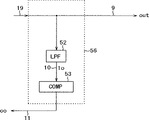
Then, use Fig. 2 that the structure example and the action of logic level converting circuit 5 are described.Logic level converting circuit 5 comprises variable inverter 51 of threshold value and decision circuitry 56, wherein, the variable inverter 51 of this threshold value is transfused to output signal 8 (the 1st signal) and the threshold setting signal (co) 11 (the 2nd signal) of VCO4, with by threshold setting signal 11 preset threshold, handle output signal 8, output signal 19 (the 3rd signal); This decision circuitry 56 is transfused to signal 19, judges the signal of being imported 19, based on the output signal (out) 9 (the 4th signal) and the threshold setting signal 11 of judged result output phase synchronous circuit.
Fig. 3 represents the 1st structure example of decision circuitry shown in Figure 2 56.The 1st decision circuitry 56 comprises low pass filter (LPF) 52 and comparator (COMP) 53, wherein, this low pass filter (LPF) 52 with signal 19 as output signal 9 output, and then, input signal 19 and the flip-flop (lo) 10 of output signal 19; Comparator (COMP) 53 is transfused to flip-flop 10, according to exporting threshold setting signal 11 with the comparative result of comparative voltage.
Fig. 4 represents the structure example of comparator 53.Comparator 53 comprises comparator 531, comparator 532 and logical circuit (LOGIC) 533, and wherein, this comparator 531 is transfused to comparative voltage Vr1 and flip-flop 10, the output comparison signal; This comparator 532 is transfused to comparative voltage Vr2 and flip-flop 10, the output comparison signal; This logical circuit (LOGIC) 533 is transfused to the comparison signal that comparison signal that comparator 531 exported and comparator 532 are exported, and generates comparative result, and the result exports threshold setting signal 11 based on the comparison.
Fig. 5 represents the input-output characteristic of comparator 53.Frequently than voltage Vr1 hour, comparative result is-1 in flip-flop 10.At this moment, comparator 53 outputs make the threshold setting signal 11 of the threshold value rising one-level of the variable inverter 51 of threshold value.Big frequently in flip-flop 10 than voltage Vr1, than Vr2 hour, comparative result is 0.At this moment, comparator 53 outputs keep the threshold setting signal 11 of the threshold value of the variable inverter 51 of threshold value.When flip-flop 10 was big than voltage Vr2 frequently, comparative result became 1.At this moment, comparator 53 outputs make the threshold value of the variable inverter 51 of threshold value reduce the threshold setting signal 11 of one-level.Carrying out this action becomes till 0 up to comparative result.After comparative result became 0, comparator 53 kept the action of threshold setting signal 11.The structure of comparator 53 also can be different with the mode of above-mentioned explanation so long as realize the structure of above-mentioned action.
At this, when signal 19 is in comparative result and becomes 0 state, claim that signal 19 is in predetermined state.Therefore, decision circuitry 56 is that benchmark is judged signal 19 with predetermined state, uses this result to generate threshold setting signal 11.
Fig. 6 represents to import the structure example of the variable inverter 51 of the 1st threshold value of output signal shown in Figure 28 and threshold setting signal 11, output signal 19, and its action is described.The variable inverter 51 of the 1st threshold value comprises: from grid input/output signal 8, from the PMOS transistor 514,515,516 of drain electrode output signal 19; Nmos pass transistor 517,518,519; By threshold setting signal 11 control, be inserted in the switch 511,512,513 (the 1st switch) between supply voltage and the PMOS transistor; And equally by 11 controls of threshold setting signal, be inserted in switch 51A, 51B, 51C (the 2nd switch) between ground connection and the nmos pass transistor.In addition, the variable inverter 51 of the 1st threshold value is as long as the control that energy passing threshold setting signal 11 moves also can be the structure different with said structure.
Fig. 7 represents the action waveforms of the logic level converting circuit 5 of present embodiment, uses the action of this action waveforms explanation logic level converting circuit 5.
At moment t0, the output signal 8 of VCO4 is transfused to logic level converting circuit 5.As initial setting, threshold setting signal 11 is the signals that are expressed as M.By being expressed as the threshold setting signal 11 of M, in the variable inverter 51 of threshold value, switch 511 and 51A become connection (ON), and other all switches become disconnection (OFF).Threshold value based on the transistor 514,517 of conducting state is Vthc1.At this, the voltage height of given threshold Vthc1 specific output signal 8 does not intersect with output signal 8.At this moment, the output signal 9 of logic level converting circuit 5 is fixed to high level (High).Thus, the flip-flop 10 of low pass filter 52 outputs becomes high level, and the comparative result of the internal signal of device 53 becomes 1 as a comparison.
As a result, at moment t1, make threshold value reduce the threshold setting signal 11 that is expressed as M-1 of one-level to variable inverter 51 outputs of threshold value from comparator 53.Received the variable inverter 51 of threshold value of the threshold setting signal 11 that is expressed as M-1,, not only made switch 511 and 51A, also made switch 51B also become connection for connecting at moment t1.As a result, threshold value changes to Vthc2 from Vthc1.
Thus, threshold value Vthc2 becomes and can intersect with output signal 8, and the output signal 9 of logic level converting circuit 5 becomes the clock signal that amplitude is Vdd, the i.e. clock signal of logic level.At this moment, the flip-flop 10 of low pass filter 52 outputs becomes 1/2Vdd, and the comparative result of the internal signal of device 53 becomes 0 as a comparison.As a result, comparator 53 makes threshold setting signal 11 remain the action of M-1, the release of logic level converting circuit 5.In addition, if, just further carry out the change of threshold value even threshold value change does not take place and the intersecting of output signal 8 yet.The change of threshold value lasted till till intersecting of generation and output signal 8 always.
At this, the voltage ratio threshold value Vthc1 height of output signal 8 is described, action and above-mentioned opposite situation.As initial setting, threshold setting signal 11 is M.By the threshold setting signal 11 as M, in the variable inverter 51 of threshold value, switch 511 and 51A become connection, and other all switches become disconnection.Threshold value based on the transistor 514,517 of conducting state is Vthc1.At this, the voltage of given threshold Vthc1 specific output signal 8 is low, does not intersect with output signal 8.Therefore, the output signal 9 of logic level converting circuit 5 is fixed to low level (Low).Thus, the flip-flop 10 of low pass filter 52 outputs becomes low level, and the comparative result of the internal signal of device 53 becomes-1 as a comparison.
As a result, make the threshold setting signal 11 that is expressed as M+1 of threshold value rising one-level to variable inverter 51 outputs of threshold value from comparator 53.Received the variable inverter 51 of threshold value of the threshold setting signal 11 that is expressed as M+1, not only made switch 511 and 51A become connection, also made switch 512 become connection.As a result, threshold value is changed to Vthc3 from Vthc1.
Thus, becoming threshold value Vthc3 can intersect with output signal 8, and the output signal 9 of logic level converting circuit 5 becomes clock signal that amplitude is Vdd, is the clock signal of logic level.At this moment, the flip-flop 10 of low pass filter 52 outputs becomes 1/2Vdd, and the comparative result of the internal signal of device 53 becomes 0 as a comparison.As a result, comparator 53 makes threshold setting signal 11 remain the action of M+1, the release of logic level converting circuit 5.In addition, with similarly above-mentioned, if, just further carry out the change of threshold value even the threshold value change does not have intersecting of generation and output signal 8 yet.The change of threshold value lasted till till intersecting of generation and output signal 8 always.
By the logic level converting circuit 5 of above present embodiment, frequency of oscillation uprises, and the amplitude of the output signal 8 of VCO4 reduces, and even voltage level changes, as output signal 9, also output amplitude is the clock signal of Vdd all the time.
In addition, the variable inverter 51 of decision circuitry 56 and threshold value can carry out various deformation respectively, by using these distortion, can realize the logic level converting circuit 5 of multiple different structure.
Fig. 8 represents the 2nd structure example of decision circuitry 56.The 2nd decision circuitry 56 comprises low pass filter 52, comparator 53 and switch (SW) 57, and wherein, this low pass filter 52 is transfused to signal 19, the flip-flop 10 of output signal 19; Comparator 53 is transfused to flip-flop 10, according to the comparative result of comparative voltage, signal 20 is judged in output threshold setting signal 11 and action; Switch (SW) 57 is transfused to signal 19 and signal 20 is judged in action, judges signal 20 controls, output signal output 9 by action.
Below, the action of the logic level converting circuit 5 of the 2nd decision circuitry 56 of having used Fig. 8 is described.
Sometime, the output signal 8 of VCO4 is transfused to logic level converting circuit 5.As initial setting, threshold setting signal 11 is M, and thus, in the variable inverter 51 of the threshold value of Fig. 6, switch 511 and 51A become connection, and other all switches become disconnection.Threshold value based on the transistor 514,517 of conducting state is Vthc1.And, as initial setting, control by action judgement signal 20, make switch 57 become disconnection.At this, threshold value Vthc1 hypothesis is voltage ratio output signal 8 height, does not intersect with output signal 8.At this moment, the output signal 19 of the variable inverter 51 of threshold value is fixed to high level.Thus, the flip-flop 10 of low pass filter 52 outputs becomes high level, and the comparative result of the internal signal of device 53 becomes 1 as a comparison.
As a result, make threshold value reduce the threshold setting signal 11 that is expressed as M-1 of one-level from comparator 53 to variable inverter 51 outputs of threshold value.Received the variable inverter 51 of threshold value of the threshold setting signal 11 that is expressed as M-1, switch 511 and 51A are connected, also made switch 51B become connection, made threshold value change to Vthc2 from Vthc1.
Thus, becoming threshold value Vthc2 can intersect with output signal 8, and the amplitude of the signal 19 of variable inverter 51 outputs of threshold value becomes Vdd.At this moment, the flip-flop 10 of low pass filter 52 outputs becomes 1/2Vdd, and the comparative result of the internal signal of device 53 becomes 0 as a comparison.As a result, comparator 53 makes threshold setting signal 11 remain the action of M-1.And then signal 20 is judged in the action that comparator 53 outputs make switch 57 become connection.Become the switch 57 of on-state, signal 19 has been exported the release of logic level converting circuit 5 as output signal 9.
At this, the voltage ratio threshold value Vthc1 height of output signal 8 is described, action and above-mentioned opposite situation.As initial setting, threshold setting signal 11 is M.By the threshold setting signal as M, in the variable inverter 51 of the 1st threshold value, switch 511 and 51A become connection, and other all switches become disconnection.Threshold value based on the transistor 514,517 of conducting state is Vthc1.And, as initial setting, control by action judgement signal 20, make switch 57 become disconnection.At this, the voltage height of threshold value Vthc1 specific output signal 8 does not intersect with output signal 8.Therefore, the output signal 19 of the variable inverter 51 of threshold value is fixed to low level.Thus, the flip-flop 10 of low pass filter 52 outputs becomes low level, and the comparative result of the internal signal of device 53 becomes-1 as a comparison.
As a result, make the threshold setting signal 11 that is expressed as M+1 of threshold value rising one-level to variable inverter 51 outputs of threshold value from comparator 53.Received the variable inverter 51 of threshold value of this threshold setting signal 11, switch 511 and 51A are connected, also made switch 512 become connection.As a result, threshold value is changed to Vthc3 from Vthc1.
Thus, becoming threshold value Vthc3 can intersect with output signal 8, and the amplitude of the signal 19 of variable inverter 51 outputs of threshold value becomes Vdd.At this moment, the flip-flop 10 of low pass filter 52 outputs becomes 1/2Vdd, and the comparative result of the internal signal of device 53 becomes 0 as a comparison.As a result, comparator 53 makes threshold setting signal 11 remain the action of M+1.And then signal 20 is judged in the action that comparator 53 outputs make switch 57 become connection.Become the switch 57 of on-state, signal 19 is exported the release of logic level converting circuit 5 as output signal 9.
In the 2nd decision circuitry 56, owing to will not be fixed as the signal of high level in above-mentioned initial actuating or be fixed as low level signal as output signal 9 output, the control of connection order (power on sequence) that therefore is transfused to the logical circuit of output signal 9 becomes easy.
Then, Fig. 9 represents the 3rd structure example of decision circuitry 56.The 3rd decision circuitry 56 shown in Figure 9 also comprises counter (CTR) 55 except signal 19 is exported as output signal 9, the counting of this counter (CTR) 55 during carrying out necessarily behind the input signal 19 is based on count results output threshold setting signal 11.55 pairs of count results of counter compare with the objective count value of expression predetermined state, and change threshold setting signal 11 is exported this threshold setting signal 11 till obtaining suitable count results.
Below, the action of the logic level converting circuit 5 of the 3rd decision circuitry 56 of having used Fig. 9 is described.
The output signal 8 of VCO4 is transfused to the variable inverter 51 of threshold value.As initial setting, threshold setting signal 11 is M, and thus, in the variable inverter 51 of the threshold value of Fig. 6, switch 511 and 51A become connection, and other all switches become disconnection.Threshold value based on the transistor 514,517 of conducting state is Vthc1.At this, the voltage height of given threshold Vthc1 specific output signal 8 does not intersect with output signal 8.At this moment, the output signal 19 of the variable inverter 51 of threshold value is fixed to high level.Carry out such processing, signal 19 is transfused to counter 55.Because output signal 19 is fixed to high level, therefore, count results is lacked than objective count value.
Because counter 55 is not distinguished the high and low level ground of output signal 19 and is counted, therefore, at first to set as initial actuating, output is with the threshold setting signal 11 of the threshold value rising one-level of the variable inverter 51 of threshold value.At this moment, threshold setting signal 11 becomes M+1.Receive the variable inverter 51 of threshold value of the threshold setting signal 11 of M+1, not only made switch 511 and 51A become connection, switch 512 is connected, made threshold value rising one-level, handled output signal 8 once more, output signal 19.Signal 19 is transfused to counter 55.Counting during 55 pairs of output signals of counter 9 are carried out necessarily compares count results and objective count value.In relatively result be under the count results situation about lacking than objective count value once more, exports raise the again threshold setting signal 11 of one-level of threshold value with the variable inverter 51 of the 1st threshold value.At this moment, threshold setting signal 11 becomes M+2.
If set 51 max-thresholds that can set of the variable inverter of threshold value, still can't obtain suitable count results, then threshold setting signal 11 just is set to M-1.Received the variable inverter 51 of threshold value of the threshold setting signal 11 of M-1, not only made switch 511 and 51A become connection, also made switch 51B become connection, made threshold value reduce one-level and handle output signal 8 once more, output signal 19.Signal 19 is transfused to counter 55.Counting during 55 pairs of output signals of counter 9 are carried out necessarily compares count results and objective count value.In relatively result be under the count results situation about lacking than objective count value once more, exports the threshold setting signal 11 that the threshold value that makes the variable inverter 51 of the 1st threshold value reduces one-level again.At this moment, threshold setting signal 11 becomes M-2.
Like this, reduce the threshold value of the variable inverter 51 of threshold value successively, when obtaining the suitable count results of the predetermined state of expression, counter 55 finishes the counting action, and keeps the threshold setting signal 11 of this moment.In addition, if obviously obtained suitable count results in the stage of rising threshold value, then counter 55 just finishes the counting action constantly at this, and keeps the threshold setting signal 11 of this moment.
The 3rd above decision circuitry 56 only is made of logical circuit, therefore, is being undertaken under the integrated situation by fine technology, and erection space diminishes, and can reduce current drain.
Then, Figure 10 represents the 4th structure example of decision circuitry 56.The 4th decision circuitry 56 shown in Figure 10 comprises counter 55 and switch 57, and wherein, the counting during this counter 55 carries out necessarily after being transfused to signal 19 is judged signal 20 based on count results output threshold setting signal 11 and action; This switch 57 is connected, is disconnected by 20 controls of action judgement signal, when connecting signal 19 is exported as output signal 9.
Below, the action of the logic level converting circuit 5 of the 4th decision circuitry 56 of having used Figure 10 is described.
The output signal 8 of VCO4 is imported into the variable inverter 51 of threshold value.As initial setting, threshold setting signal 11 is M, and thus, in the variable inverter 51 of the threshold value of Fig. 6, switch 511 and 51A become connection, and other all switches become disconnection.Threshold value based on the transistor 514,517 of conducting state is Vthc1.And, as initial setting, control by action judgement signal 20, make switch 57 become disconnection.At this, the voltage height of given threshold Vthc1 specific output signal 8 does not intersect with output signal 8.At this moment, the output signal 19 of the variable inverter 51 of threshold value is fixed to high level.Carry out such processing, signal 19 is imported into counter 55.Because output signal 19 is fixed to high level, so count results is lacked than objective count value.
Because counter 55 is not distinguished the high and low level ground of output signal 19 and is counted, therefore, at first to set as initial actuating, output makes the threshold setting signal 11 of the threshold value rising one-level of the variable inverter 51 of threshold value.At this moment, threshold setting signal 11 becomes M+1.Receive the variable inverter 51 of threshold value of the threshold setting signal 11 of M+1, switch 511 and 51A are connected, also made switch 512 become connection, made threshold value rising one-level, handled output signal 8 once more, output signal 19.Signal 19 is imported into counter 55.Counting during 55 pairs of output signals of counter 9 are carried out necessarily compares count results and objective count value.In relatively result is under the count results situation about lacking than objective count value once more, and output makes raise the again threshold setting signal 11 of one-level of the threshold value of the variable inverter 51 of threshold value.At this moment, threshold setting signal 11 becomes M+2.
If set 51 max-thresholds that can set of the variable inverter of threshold value, still can't obtain suitable count results, then the threshold setting signal is set to M-1.Receive the variable inverter 51 of threshold value of the threshold setting signal 11 of M-1, switch 511 and 51A are connected, also made switch 51B become connection, made threshold value reduce one-level, handled output signal 8 once more, output signal 19.Signal 19 is imported into counter 55.Counting during 55 pairs of output signals of counter 9 are carried out necessarily compares count results and objective count value.In relatively result is that output makes the threshold value of the variable inverter 51 of the 1st threshold value reduce the threshold setting signal 11 of one-level again under the count results situation about lacking than objective count value once more.At this moment, threshold setting signal 11 becomes M-2.
Like this, reduce the threshold value of the variable inverter 51 of threshold value successively, when obtaining the suitable count results of the predetermined state of expression, counter 55 finishes the counting action, and keeps the threshold setting signal 11 of this moment.In addition, if obviously obtained suitable count results in the stage of the threshold value that raises successively, then counter 55 just finishes the counting action constantly at this, and keeps the threshold setting signal 11 of this moment.Because of having obtained the moment that suitable count results finishes to count action, signal 20 is judged in the action that counter 55 outputs make switch 57 become connection at counter 55.Become the switch 57 of on-state, signal 19 is exported the release of logic level converting circuit 5 as output signal 9.
In the 4th above decision circuitry 56, owing to will not be fixed as the signal of high level in above-mentioned initial actuating or be fixed as low level signal as output signal 9 outputs, the energising time sequence control that therefore is transfused to the logical circuit of output signal 9 becomes easy.And the 4th decision circuitry 56 only is made of logical circuit, therefore, is being undertaken under the integrated situation by fine technology, and erection space diminishes, and can reduce current drain.
Then, Figure 11 represents the 5th structure example of decision circuitry 56.The 5th decision circuitry 56 shown in Figure 11 is except exporting signal 19 as output signal 9, also comprise attenuator (PAD) 58A and tester (TST) 58 that chip is outer, wherein, this attenuator 58A exports setting signals based on this measurement result to tester 58 in chip external pelivimetry output signal 9; This tester (TST) 58 is transfused to above-mentioned setting signal, output threshold setting signal 11.
Below, the action of the 5th decision circuitry 56 is described.In chip external pelivimetry output signal 9, is the situation of high level fix signal under in measurement result by attenuator 58A, for the threshold value that makes the variable inverter 51 of threshold value reduces one-level, exports setting signals from attenuator 58A to tester 58.Receive the tester 58 of this setting signal, set the threshold setting signal 11 that the threshold value that makes the variable inverter 51 of threshold value reduces one-level.After having set threshold setting signal 11, measure output signal 9 in chip exterior once more.Like this setting threshold setting signal 11, but make that output signal 9 becomes the best signal of duty ratio (duty), promptly becomes predetermined state in the scope of the threshold value of the variable inverter 51 of setting threshold.At this, so-called duty ratio is to represent the ratio of the interval of high level signal with respect to the interval in 1 cycle of signal with percentage.
Then, Figure 12 represents input/output signal 8 and threshold setting signal 11 and the 2nd structure example of the variable inverter 51 of threshold value shown in Figure 2 of output signal 19.The variable inverter 51 of the 2nd threshold value comprises: the inverter 501,502,503,504,505 of output signal 19; Be present between output signal 8 and the inverter 501,502,503,504,505, by switch 506,507,508,509, the 50A of threshold setting signal 11 controls.
The variable inverter 51 of the 2nd threshold value is transfused to output signal 8 and threshold setting signal 11, respectively the output signal of inverter 501,502,503,504,505 is exported as signal 19.Inverter 501,502,503,504,505 is set to threshold value and has nothing in common with each other.
Below, the action of having used variable inverter 51 of the 2nd threshold value shown in Figure 12 and the 1st logic level converting circuit 5 decision circuitry 56, shown in Figure 2 shown in Figure 3 is described.
At moment t0, output signal 8 is imported into logic level converting circuit 5.As initial setting, threshold setting signal 11 is M, and thus, in the variable inverter 51 of the 2nd threshold value, switch 508 is for connecting, and other all switches become disconnection.At this, suppose the voltage height of the threshold ratio output signal 8 of the inverter 503 that is connected with switch 508, threshold value does not intersect with output signal 8.At this moment, signal 19 is fixed to high level.Thus, the flip-flop 10 of low pass filter 52 outputs becomes high level, and the comparative result of the internal signal of device 53 becomes 1 as a comparison.
As a result, make threshold value reduce the threshold setting signal 11 that is expressed as M-1 of one-level from comparator 53 to variable inverter 51 outputs of the 2nd threshold value.Received the variable inverter 51 of the 2nd threshold value of the threshold setting signal 11 of M-1, switch 508 is disconnected, made switch 509 become connection.
Thus, the threshold value that becomes the inverter 504 that is connected with switch 509 can intersect with output signal 8, and the output signal 9 of logic level converting circuit 5 becomes the clock signal that amplitude is the logic level of Vdd.At this moment, the flip-flop 10 of low pass filter 52 outputs becomes 1/2Vdd, and the comparative result of the internal signal of device 53 becomes 0 as a comparison.As a result, comparator 53 makes threshold setting signal 11 remain the action of M-1, as the release of logic level converting circuit 5.
At this, the threshold value height of the voltage ratio inverter 503 of output signal 8 is described, action and above-mentioned opposite situation.As initial setting, the threshold setting signal is M.By the threshold setting signal as M, in the variable inverter 51 of the 2nd threshold value, switch 503 is connected, and other all switches become disconnection.The voltage of threshold ratio output signal 8 of supposing inverter 503 is low, does not intersect with output signal 8.Therefore, signal 19 is fixed to low level.Thus, the flip-flop 10 of low pass filter 52 outputs becomes low level, and the comparative result of the internal signal of device 53 becomes-1 as a comparison.
As a result, make the threshold setting signal 11 of the M+1 of threshold value rising one-level to variable inverter 51 outputs of threshold value from comparator 53.Received the variable inverter 51 of the 2nd threshold value of the threshold setting signal 11 of M+1, made switch 508 become disconnection, made switch 507 become connection.Thus, the threshold value that becomes the inverter 502 that is connected with switch 507 can intersect with output signal 8, and the output signal 9 of logic level converting circuit 5 becomes the clock signal that amplitude is the logic level of Vdd.At this moment, the flip-flop 10 of low pass filter 52 outputs becomes 1/2Vdd, and the comparative result of the internal signal of device 53 becomes 0 as a comparison.As a result, comparator 53 makes threshold setting signal 11 remain the action of M+1, the release of logic level converting circuit 5.
Then, the action of having used variable inverter 51 of the 2nd threshold value shown in Figure 12 and the 2nd logic level converting circuit 5 decision circuitry 56, Fig. 2 shown in Figure 8 is described.
Be imported into logic level converting circuit 5 in output signal 8 sometime.As initial setting, threshold setting signal 11 is M, and then, control by action judgement signal 20, make switch 57 become disconnection.Under this state, in the variable inverter 51 of the 2nd threshold value, switch 508 becomes connection, and other all switches become disconnection.At this, suppose the voltage height of the threshold ratio output signal 8 of inverter 503, do not intersect with output signal 8.At this moment, the output signal 19 of the variable inverter 51 of the 2nd threshold value is fixed to high level.Thus, the flip-flop 10 of low pass filter 52 outputs becomes high level, and the comparative result of the internal signal of device 53 becomes 1 as a comparison.
As a result, make threshold value reduce the threshold setting signal of the M-1 of one-level from comparator 53 to variable inverter 51 outputs of the 2nd threshold value.Received the variable inverter 51 of the 2nd threshold value of the threshold setting signal 11 of M-1, made switch 508 become disconnection, made switch 509 become connection.
Thus, with inverter 504 that switch 509 is connected in, its threshold value becomes and can intersect with output signal 8, the output signal 9 of logic level converting circuit 5 becomes the clock signal that amplitude is the logic level of Vdd.At this moment, the flip-flop 10 of low pass filter 52 outputs becomes 1/2Vdd, and the comparative result of the internal signal of device 53 becomes 0 as a comparison.As a result, comparator 53 makes threshold setting signal 11 remain the action of M-1.And then signal 20 is judged in the action that comparator 53 outputs are connected switch 57.Become the switch 57 of on-state, signal 19 has been exported as output signal 9, as the release of logic level converting circuit 5.
At this, illustrate that the voltage of threshold ratio output signal 8 of inverter 503 is low, action and above-mentioned opposite situation.As initial setting, threshold setting signal 11 is M, and then, control by action judgement signal 20, make switch 57 become disconnection.Under this state, in the variable inverter 51 of the 2nd threshold value, switch 508 becomes connection, and other all switches become disconnection.At this, the voltage of the threshold ratio output signal 8 of inverter 503 is low, does not intersect with output signal 8.Therefore, signal 19 is fixed to low level.Thus, the flip-flop 10 of low pass filter 52 outputs becomes low level, and the comparative result of the internal signal of device 53 becomes-1 as a comparison.
As a result, make the threshold setting signal 11 of the M+1 of threshold value rising one-level to variable inverter 51 outputs of the 2nd threshold value from comparator 53.Received the variable inverter 51 of the 2nd threshold value of this threshold setting signal 11, made switch 508 become disconnection, made switch 507 become connection.As a result, the threshold value that becomes inverter 504 can intersect with output signal 8, and the amplitude of the signal 19 of variable inverter 51 outputs of the 2nd threshold value becomes Vdd.At this moment, the flip-flop 10 of low pass filter 52 outputs becomes 1/2Vdd, and the comparative result of the internal signal of device 53 becomes 0 as a comparison.As a result, comparator 53 makes threshold setting signal 11 remain the action of M+1.And then signal 20 is judged in the action that comparator 53 outputs make switch 57 become connection.Become the switch 57 of on-state, signal 19 has been exported the release of logic level converting circuit 5 as output signal 9.
Below, the 2nd action of having used variable inverter 51 of the 2nd threshold value shown in Figure 12 and the 2nd logic level converting circuit 5 decision circuitry 56, Fig. 2 shown in Figure 8 is described.
Be imported into logic level converting circuit 5 in the output signal 8 of VCO4 sometime.As initial setting, switch 506,507,508,509,50A all connect.And, as initial setting, control by action judgement signal 20, make switch 57 become disconnection.At this moment, the inverter 501,502,503,504,505 that is transfused to output signal 8 output signal 19 separately.Be transfused to the low pass filter 52 of all output signals 19, exported the flip-flop 10 of each output signal 19.Comparator 53 compares each flip-flop 10 and comparative voltage, output threshold setting signal 11, and wherein, this threshold setting signal 11 is controlled and is made and only select comparative result to become 0 inverter, and other inverter is not moved.And then signal 20, the release of logic level converting circuit 5 are judged in the action that comparator 53 outputs are connected switch 57.
Then, the action of having used variable inverter 51 of the 2nd threshold value shown in Figure 12 and the 3rd logic level converting circuit 5 decision circuitry 56, Fig. 2 shown in Figure 9 is described.
The output signal 8 of VCO4 is imported into the variable inverter 51 of the 2nd threshold value.As initial setting, threshold setting signal 11 is M, and thus, in the variable inverter 51 of the 2nd threshold value, switch 508 is connected, and other all switches become disconnection.At this, suppose the voltage height of the threshold ratio output signal 8 of the inverter 503 that is connected with switch 508, do not intersect with output signal 8.At this moment, the signal 19 of variable inverter 51 outputs of the 2nd threshold value is fixed to high level.The signal 19 of having accepted such processing is imported into counter 55.Because output signal 19 is fixed to high level, so count results is lacked than objective count value.
Because counter 55 is not distinguished the high and low level ground of output signal 19 and counted, therefore, at first as initial setting, output makes the threshold setting signal 11 of the threshold value rising one-level of the variable inverter 51 of the 2nd threshold value.At this moment, threshold setting signal 11 becomes M+1.Received the variable inverter 51 of the 2nd threshold value of the threshold setting signal 11 of M+1, made switch 508 become disconnection, made switch 507 become connection.The variable inverter 51 of the 2nd threshold value is handled output signal 8, output signal 19 so once more.Signal 19 is imported into counter 55.Counting during 55 pairs of signals of counter 19 carry out necessarily compares count results and objective count value.In relatively result be under the count results situation about lacking than objective count value once more, exports raise the again threshold setting signal 11 of one-level of the threshold value that makes the variable inverter 51 of the 2nd threshold value.At this moment, threshold setting signal 11 becomes M+2.Received the variable inverter 51 of the 2nd threshold value of the threshold setting signal of M+2, switch 507 is disconnected, switch 506 is connected.
If set 51 max-thresholds that can set of the variable inverter of the 2nd threshold value, also can't obtain suitable count results, then next threshold setting signal 11 is set at M-1.Receive the variable inverter 51 of the 2nd threshold value of the threshold setting signal of M-1, handled output signal 8 so once more, output signal 19.Signal 19 is imported into counter 55.Counting during 55 pairs of signals of counter 19 carry out necessarily compares count results and objective count value.In relatively result is that output makes the threshold value of the variable inverter 51 of the 2nd threshold value reduce the threshold setting signal 11 of one-level again under the count results situation about lacking than objective count value once more.At this moment, threshold setting signal 11 becomes M-2.
So, reduce the threshold value of the variable inverter 51 of threshold value successively, when obtaining suitable count results, counter 55 finishes the counting action, and keeps the threshold setting signal 11 of this moment.In addition, if obtained suitable count results in the stage of rising threshold value, then counter 55 finishes the counting action constantly at this, and keeps the threshold setting signal 11 of this moment.
Then, the action of having used variable inverter 51 of the 2nd threshold value shown in Figure 12 and the 4th logic level converting circuit 5 decision circuitry 56, Fig. 2 shown in Figure 10 is described.
The output signal 8 of VCO4 is imported into the variable inverter 51 of the 2nd threshold value.As initial setting, threshold setting signal 11 is M, and thus, in the variable inverter 51 of the 2nd threshold value of Figure 12, switch 508 is connected, and other all switches disconnect.And, as initial setting, control by action judgement signal 20, make switch 57 for disconnecting.At this, suppose the voltage height of the threshold ratio output signal 8 of the inverter 503 that is connected with switch 508, do not intersect with output signal 8.At this moment, the output signal 19 of the variable inverter 51 of the 2nd threshold value is fixed to high level.After having carried out such processing, signal 19 is imported into counter 55.Because output signal 19 is fixed to high level, so count results is lacked than objective count value.
Because counter 55 is not distinguished the high and low level ground of output signal 19 and is counted, therefore, at first to set as initial actuating, output makes the threshold setting signal 11 of the threshold value rising one-level of the variable inverter 51 of threshold value.At this moment, threshold setting signal 11 becomes M+1.Received the variable inverter 51 of the 2nd threshold value of the threshold setting signal 11 of M+1, made switch 508 become disconnection, made switch 507 become connection.The variable inverter 51 of the 2nd threshold value is handled output signal 8, output signal 19 so once more.Signal 19 is imported into counter 55.Counting during 55 pairs of signals of counter 19 carry out necessarily compares count results and objective count value.In relatively result is under the count results situation about lacking than objective count value once more, and output makes raise the again threshold setting signal 11 of one-level of the threshold value of the variable inverter 51 of the 2nd threshold value.At this moment, threshold setting signal 11 becomes M+2.Received the variable inverter 51 of the 2nd threshold value of the threshold setting signal 11 of M+2, switch 507 is disconnected, switch 506 is connected.
If set 51 max-thresholds that can set of the variable inverter of the 2nd threshold value, still can't obtain suitable count results, then next threshold setting signal 11 is set at M-1.Received the variable inverter 51 of the 2nd threshold value of the threshold setting signal 11 of M-1, made switch 506 become disconnection, made switch 509 become connection.So, the variable inverter 51 of the 2nd threshold value is handled output signal 8, output signal 19 once more.Signal 19 is imported into counter 55.Counting during 55 pairs of signals of counter 19 carry out necessarily compares count results and objective count value.In relatively result is that output makes the threshold value of the variable inverter 51 of the 2nd threshold value reduce the threshold setting signal 11 of one-level again under the count results situation about lacking than objective count value once more.At this moment, threshold setting signal 11 becomes M-2.
So, reduce the threshold value of the variable inverter 51 of threshold value successively, when obtaining suitable count results, counter 55 finishes the counting action, and keeps the threshold setting signal 11 of this moment.And according to having obtained the moment that this situation of suitable count results finishes to count action, switch 57 becomes connection at counter 55, and counter 55 output actions are judged signal 20.The switch 57 that becomes on-state is exported the release of logic level converting circuit 5 with signal 19 as output signal 9.
Below, the 2nd action of having used variable inverter 51 of the 2nd threshold value shown in Figure 12 and the 4th logic level converting circuit 5 decision circuitry 56, Fig. 2 shown in Figure 10 is described.
Be imported into logic level converting circuit 5 in output signal 8 sometime.As initial setting, switch 506,507,508,509,50A all become connection.And, as initial setting, control by action judgement signal 20, make switch 57 become disconnection.Under this state, the inverter 501,502,503,504,505 of having imported output signal 8 is output signal output 19 separately.Imported the counter 55 of all output signals 19, signal 19 has been carried out counting during certain, count results and objective count value have been compared.Comparator 55 output threshold setting signals 11, wherein, this threshold setting signal 11 is controlled the feasible inverter of only selecting comparative result the best, and other inverter is not moved.And then signal 20, the release of logic level converting circuit 5 are judged in the action that counter 55 outputs are connected switch 57.
Then, the action of having used variable inverter 51 of the 2nd threshold value shown in Figure 12 and the 5th logic level converting circuit 5 decision circuitry 56, Fig. 2 shown in Figure 11 is described.
In the variable inverter 51 of the 2nd threshold value, as initial setting, switch 508 becomes connection, and other all switches become disconnection.At this moment, measure output signal 9 by attenuator 58A in chip exterior.In measurement result is under the situation of high level fix signal, for the threshold value that makes the variable inverter 51 of threshold value reduce one-level from the attenuator 58A of chip exterior to tester 58 output setting signals.Receive the tester 58 of setting signal, set the threshold setting signal 11 that the threshold value that makes the variable inverter 51 of the 2nd threshold value reduces one-level.After having set threshold setting signal 11, measure output signal 9 in chip exterior once more.So, setting threshold setting signal 11, but make that output signal 9 becomes the signal of duty ratio the best in the scope of the threshold value of the variable inverter 51 of setting threshold.
Above-mentioned each logic level converting circuit can make the scale of erection space diminish, and then, for the incoming frequency of the wide region from the low frequency to the high frequency, can both move with low-power consumption.Therefore, can be installed in the large scale integrated circuit.And above-mentioned logic level converting circuit also carries out the duty cycle correction action, therefore, has had the phase locking circuit of above-mentioned logic level converting circuit, can be at the incoming frequency of the wide region from the low frequency to the high frequency, and output duty cycle is maintained 50% signal.
<embodiment 2 〉
Figure 13 represents embodiments of the invention 2.As shown in figure 13, the phase locking circuit of present embodiment comprises: phase frequency comparator 1; Charge pump 2; Loop filter 3; Receive direct voltage and adjust signal (idco) 15, adjust the VCO24 of the DC level of output signal (fvco) 8; Output dc voltage is adjusted signal 15, and output signal 8 is converted to the logic level converting circuit 25 of the output signal 9 that follow-up logical circuit (not shown) can correctly discern; The output frequency of VCO24 is carried out the frequency divider 6 of frequency division.
The phase locking circuit of present embodiment carries out the action same with the phase locking circuit of embodiment 1, so omit the explanation to it.
Figure 14 represents the structure example of VCO24.VCO24 is transfused to control voltage vc and direct voltage is adjusted signal 15, output signal output 8.VCO24 comprises voltage-current converter circuit 241, current control oscillator 247 and differential single-ended change-over circuit 245, and wherein, this voltage-current converter circuit 241 will be controlled voltage vc and convert electric current to; The Current Regulation retardation that current control oscillator 247 generates by voltage conversion circuit 241; Differential single-ended change-over circuit 245 is transfused to the differential output signal 16,17 of current control oscillator 247 and direct voltage and adjusts signal 15, converts the differential output signal 16,17 of current control oscillator 247 to mono signal.Differential single-ended change-over circuit 245 is adjusted signal 15 according to direct voltage and is adjusted flip-flop, and mono signal is exported as output signal 8.
Figure 15 represents the structure example of current control oscillator 247.Current control oscillator 247 is that the delay circuit 242 that will adjust retardation according to drive current connects into ring-type and constitutes.In Figure 15, current control oscillator 247 constitutes by the delay circuit 242 that connects odd number section (3 sections).
Figure 16 represents the structure example of differential single-ended change-over circuit 245.Differential single-ended change-over circuit 245 comprises the transistor 2451 that generates drive current according to bias voltage signal vb, receives the transistor 2452,2453 of differential wave (vi1) 16, (vi2) 17, and load transistor 2454,2455.At the A point, output signal 8 is adjusted signal 15 according to direct voltage and is adjusted DC level, outputs to logic level converting circuit 25.
Structure about VCO24, voltage-current converter circuit 241, current control oscillator 247 and differential single-ended change-over circuit 245, so long as input control voltage vc, the structure that obtains desirable frequency of oscillation by output signal 8 gets final product, can be different with the device of above explanation.
Then, the syndeton example of differential single-ended change-over circuit 245 with logic level converting circuit 25 is illustrated among Figure 17 A, the action of differential single-ended change-over circuit 245 and logic level converting circuit 25 is described.Logic level converting circuit 25 comprises inverter 251 and decision circuitry (JC) 59, and wherein, this inverter 251 is transfused to the output signal 8 output signal, VCO24 as differential single-ended change-over circuit 245, output signal 19; This decision circuitry (JC) 59 is transfused to signal 19, and signal 19 is judged, adjusts signal 15 according to judged result output signal output 9 and direct voltage.Direct voltage is adjusted the A point that signal 15 is provided to differential single-ended change-over circuit 245.
In addition, because the input and output of differential single-ended change-over circuit 245 and logic level converting circuit 25 are connected by 1 wiring, therefore, also it doesn't matter even the A point is positioned at the input side of logic level converting circuit 25.In this case, direct voltage is adjusted the A point that signal 15 is provided to the inside of logic level converting circuit 25, adjusts the DC level of the output signal 8 that offers inverter 251.This processing also can be shown in Figure 17 B like that, the A point configuration adder 252 in the inside of logic level converting circuit 25 is adjusted direct voltage by adder 252 the output signal addition of signal 15 and differential single-ended change-over circuit 245.By adder 252, except electric current being carried out additional calculation and adjusting the DC level, direct voltage can also be adjusted the signal of signal 15 as voltage, voltage is carried out additional calculation and adjusts DC level.Below use Figure 17 A to describe.
The 1st structure example of the decision circuitry 59 shown in Figure 17 A is illustrated among Figure 18.The 1st decision circuitry 59 comprises low pass filter 52, comparator 53 and DA (Digital toAnalog) transducer (DAC) 254, wherein, this low pass filter 52 with signal 19 as output signal 9 output, and input signal 19 and the flip-flop 10 of output signal 19; This comparator (COMP) 53 is transfused to flip-flop 10, exports threshold setting signal 11 according to the result with the comparative voltage comparison; 254 pairs of threshold setting signals of this DA (Digital to Analog) transducer (DAC) 11 carry out analog-converted, and output dc voltage is adjusted signal 15.
Below, illustrate and used the differential single-ended change-over circuit 245 the 1st decision circuitry 59 shown in Figure 180, shown in Figure 17 A and the action of logic level converting circuit 25.
As initial setting, DA transducer 254 not output dc voltage is adjusted signal 15.At a time, differential single-ended change-over circuit 245 is transfused to differential wave 16,17, the output signal 8 of output VCO24.Output signal 8 is imported into logic level converting circuit 25.The threshold value of inverter 251 is Vthi.At this, suppose that the threshold value of voltage ratio inverter 251 of output signal 8 is low, the threshold value with inverter 251 does not intersect.At this moment, signal 19 is fixed to high level.Thus, the flip-flop 10 of low pass filter 52 outputs becomes high level, and the comparative result of the internal signal of device 53 becomes 1 as a comparison.
As a result, comparator 53 is exported the threshold setting signal 11 of the M+1 of the flip-flop rising one-level that makes the output signal 8 in the differential single-ended change-over circuit 245.Received DA transducer 254, made flip-flop rising direct voltage one-level, current value I of output signal 8 adjust signal 15 to differential single-ended change-over circuit 245 outputs as the threshold setting signal 11 of M+1.The direct voltage of having imported current value I is adjusted the differential single-ended change-over circuit 245 of signal 15, makes the flip-flop of output signal 8 increase current value I at the A point.At this moment, the alternating component of output signal 8 does not change.Increase the output signal 8 of flip-flop like this, be imported into inverter 251 once more.
Carrying out above-mentioned action repeatedly becomes and can intersect with the threshold value of inverter 251 up to output signal 8.Become to intersect with the threshold value of inverter 251 time in output signal 8, comparator 53 is in order to keep this state (predetermined state), former state keep being set the threshold value of output signal 8 and inverter 251 is intersected threshold setting signal 11, the release of logic level converting circuit 25.
At this, the threshold value height of the voltage ratio inverter 251 of output signal 8 is described, action and above-mentioned opposite situation.As initial setting, DA transducer 254 not output dc voltage is adjusted signal 15.At a time, differential single-ended change-over circuit 245 is transfused to differential wave 16,17, output signal output 8.Output signal 8 is imported into logic level converting circuit 25.At this, the threshold value of inverter 251 is Vthi, because the threshold value comparison with voltage height of output signal 8 and inverter 251, therefore, output signal 8 is not crossing with the threshold value of inverter 251.Therefore, signal 19 is fixed to low level.Thus, the flip-flop 10 of low pass filter 52 outputs becomes low level, and the comparative result of the internal signal of device 53 becomes-1 as a comparison.
As a result, comparator 53 makes the flip-flop of output signal 8 reduce the threshold setting signal 11 that is expressed as M-1 of one-level to differential single-ended change-over circuit 245 outputs.Received the DA transducer 254 of the threshold setting signal 11 of M-1, adjusted signal 15 to the direct voltage that differential single-ended change-over circuit 245 outputs make the flip-flop of output signal 8 reduce the current value-I of one-level.The direct voltage that has been transfused to current value-I is adjusted the differential single-ended change-over circuit 245 of signal, makes the flip-flop of output signal 8 increase current value-I at the A point, even it reduces current value I.At this moment, the alternating component of output signal 8 does not change.Reduce the output signal 8 of flip-flop like this, be input to inverter 251 once more.
Carrying out above-mentioned action repeatedly becomes and can intersect with the threshold value of inverter 251 up to output signal 8.Become when intersecting in output signal 8 with the threshold value of inverter 251, comparator 53 is in order to keep this state (predetermined state), former state keep being set the threshold value of output signal 8 and inverter 251 is intersected threshold setting signal 11, the release of logic level converting circuit 25.
Then, the 2nd structure example of the decision circuitry 59 that Figure 17 A is put down in writing is illustrated among Figure 19.The 2nd decision circuitry 59 comprises low pass filter 52, comparator 53, switch 57 and DA transducer 254, and wherein, this low pass filter 52 is transfused to signal 19 and the flip-flop 10 of output signal 19; This comparator 53 is transfused to flip-flop 10, exports threshold setting signal 11 and action judgement signal 20 according to the result with the comparative voltage comparison; This switch 57 is judged signal 20 control connections by moving, is disconnected, and when on-state signal 19 is exported as output signal 9; 254 pairs of threshold setting signals of this DA transducer 11 carry out analog-converted, and output dc voltage is adjusted signal 15.
Below, illustrate and used the differential single-ended change-over circuit 245 the 2nd decision circuitry 59 shown in Figure 19, Figure 17 A and the action of logic level converting circuit 25.
As initial setting, DA transducer 254 not output dc voltage is adjusted signal 15.And, as initial setting, judge that by action the switch 57 of signal 20 controls is an off-state.At a time, differential single-ended change-over circuit 245 is transfused to differential wave 16,17, and output signal output 8.Output signal 8 is imported into logic level converting circuit 25.At this, the threshold value of inverter 251 is Vthi, supposes that the threshold value of voltage ratio inverter 251 of output signal 8 is low, and the threshold value with inverter 251 does not intersect.At this moment, signal 19 is fixed to high level.Thus, the output signal 10 of low pass filter 52 outputs becomes high level, and the comparative result of the internal signal of device 53 becomes 1 as a comparison.
As a result, comparator 53 makes the threshold setting signal 11 that is expressed as M+1 of the flip-flop rising one-level of output signal 8 to differential single-ended change-over circuit 245 outputs.Received the DA transducer 254 of the threshold setting signal 11 of M+1, adjusted signal 15 to the direct voltage that differential single-ended change-over circuit 245 is exported the current value I of the flip-flop rising one-level that makes output signal 8.The direct voltage of having imported current value I is adjusted the differential single-ended change-over circuit 245 of signal 15, makes the flip-flop of output signal 8 increase current value I at the A point.At this moment, the alternating component of output signal 8 does not change.Increase the output signal 8 of flip-flop like this, be input to inverter 251 once more.
Carrying out above-mentioned action repeatedly becomes and can intersect with the threshold value of inverter 251 up to output signal 8.Become when intersecting with the threshold value of inverter 251 in output signal 8, comparator 53 is in order to keep this state (predetermined state), carries out former state and keeps being set to such an extent that make the action of the threshold setting signal 11 that the threshold value of output signal 8 and inverter 251 intersects.And then comparator 53 becomes at 0 o'clock at the comparative result as internal signal, and signal 20 is judged in the action that output makes switch 57 become connection.Become the switch 57 of on-state, signal 19 has been exported the release of logic level converting circuit 25 as output signal 9.
At this, the threshold value comparison with voltage height of output signal 8 and inverter 251 is described, action and above-mentioned opposite situation.As initial setting, DA transducer 254 not output dc voltage is adjusted signal 15.And switch 57 judges that by action the control of signal 20 becomes disconnection.At a time, differential single-ended change-over circuit 245 is transfused to differential wave 16,17 and output signal output 8.Output signal 8 is imported into logic level converting circuit 25.The threshold value of inverter 251 is Vthi.At this, suppose the threshold value height of the voltage ratio inverter 251 of output signal 8, the threshold value with inverter 251 does not intersect.At this moment, signal 19 is fixed to low level.Thus, the output signal 10 of low pass filter 52 outputs becomes low level, and the comparative result of the internal signal of device 53 becomes-1 as a comparison.
As a result, comparator 53 reduces the threshold setting signal 11 of the M-1 of one-level as the flip-flop that makes output signal 8, is expressed as the signal of M-1 to differential single-ended change-over circuit 245 outputs.Received the DA transducer 254 of the threshold setting signal 11 of M-1, adjusted signal 15 to the direct voltage that differential single-ended change-over circuit 245 outputs make the flip-flop of output signal 8 reduce the current value-I of one-level.Imported the differential single-ended change-over circuit 245 of adjusting the current value-I of signal 15 as direct voltage, made the flip-flop of output signal 8 increase current value-I at the A point, even flip-flop reduces current value I.At this moment, the alternating component of output signal 8 does not change.Reduce the output signal 8 of flip-flop like this, be input to inverter 251 once more.
Carrying out above-mentioned action repeatedly becomes and can intersect with the threshold value of inverter 251 up to output signal 8.Become when intersecting with the threshold value of inverter 251 in output signal 8, comparator 53 is in order to keep this state (predetermined state), carries out former state and keeps being set to such an extent that make the action of the threshold setting signal 11 that the threshold value of output signal 8 and inverter 251 intersects.And then comparator 53 becomes at 0 o'clock at the comparative result as internal signal, and signal 20 is judged in the action that output makes switch 57 become connection.Become the switch 57 of on-state, signal 19 has been exported the release of logic level converting circuit 25 as output signal 9.
Then, the 3rd structure example of the decision circuitry 59 that Figure 17 A is put down in writing is illustrated among Figure 20.The 3rd decision circuitry 59 comprises counter 55 and DA transducer 254, and wherein, this counter 55 is exported signal 19 as output signal 9, and the counting input signal 19 backs are carried out necessarily to signal 19 during, based on count results output threshold setting signal 11; 254 pairs of threshold setting signals of this DA transducer 11 carry out analog-converted, and output dc voltage is adjusted signal 15.
Below, illustrate and used the differential single-ended change-over circuit 245 the 3rd decision circuitry 59 shown in Figure 20, Figure 17 A and the action of logic level converting circuit 25.
As initial setting, DA transducer 254 not output dc voltage is adjusted signal 15.At a time, differential single-ended change-over circuit 245 is transfused to differential wave 16,17, output signal output 8.Output signal 8 is imported into logic level converting circuit 25.The threshold value of inverter 251 is Vthi.At this, suppose that the threshold value of voltage ratio inverter 251 of output signal 8 is low, the threshold value with inverter 251 does not intersect.At this moment, signal 19 is fixed to high level.Signal 19 is imported into counter 55.Because signal 19 is fixed to high level, therefore, count results is lacked than objective count value.
Because counter 55 is that the high and low level ground of not distinguishing output signal 19 is counted, therefore, at first to set as initial actuating, output makes the threshold setting signal 11 of the flip-flop rising one-level of output signal 8.At this moment, threshold setting signal 11 becomes M+1.Received the DA transducer 254 of the threshold setting signal 11 of M+1, adjusted signal 15 to the direct voltage that differential single-ended change-over circuit 245 is exported the current value I of the flip-flop rising one-level that makes output signal 8.Imported the differential single-ended change-over circuit 245 of adjusting the current value I of signal 15 as direct voltage, made the flip-flop of output signal 8 increase current value I at the A point.At this moment, the alternating component of output signal 8 does not change.Increase the output signal 8 of flip-flop like this, be input to inverter 251 once more.Inverter 251 output signals 19 of output signal 8 have been imported.Signal 19 is imported into counter 55.Counting during 55 pairs of output signals of counter 9 are carried out necessarily compares count results and objective count value.In relatively result is under the count results situation about lacking than objective count value once more, makes the threshold setting signal 11 of the flip-flop rising one-level of output signal 8 to differential single-ended change-over circuit 245 outputs.At this moment, threshold setting signal 11 becomes M+2.
Even adjust signal 15 if set the direct voltage of 254 maximums that can set of DA transducer, also can't obtain suitable count results, be M-1 next then with the threshold setting signal sets.Received the DA transducer 254 of the threshold setting signal 11 of M-1, adjusted signal 15 to the direct voltage that differential single-ended change-over circuit 245 outputs make the flip-flop of output signal 8 reduce the current value-I of one-level.The direct voltage of having imported current value-I is adjusted the differential single-ended change-over circuit 245 of signal 15, makes the flip-flop of output signal 8 increase current value-I at the A point, even flip-flop reduces current value I.At this moment, the alternating component of output signal 8 does not change.Inverter 251 quilts are input/output signal 8 once more, output signal 19.Signal 19 is imported into counter 55.Counting during 55 pairs of output signals of counter 9 are carried out necessarily compares count results and objective count value.In relatively result is that output is set to the threshold setting signal 11 that the flip-flop that makes output signal 8 reduces one-level again under the count results situation about lacking than objective count value once more.At this moment, threshold setting signal 11 becomes M-2.
So, reduce the flip-flop of output signal 8 successively, when obtaining the suitable count results of the predetermined state of expression, counter 55 finishes the counting action, keeps the threshold setting signal 11 of this moment.In addition, obviously, if obtained suitable count results in the stage of the threshold value that raises successively, then counter 55 finishes the counting action constantly at this, and keeps the threshold setting signal 11 of this moment.Thus, the release of logic level converting circuit 25.
Then, the 4th structure example of the decision circuitry 59 that Figure 17 A is put down in writing is illustrated among Figure 21.The 4th decision circuitry 59 comprises counter 55 and switch 57, and wherein, this counter 55 is judged signal 20 at the counting that is transfused to signal 19 backs are carried out necessarily to signal 19 during based on count results output threshold setting signal 11 and action; This switch 57 is connected, is disconnected by 20 controls of action judgement signal, when connecting signal 19 is exported as output signal 9.
Below, illustrate and used the differential single-ended change-over circuit 245 the 4th decision circuitry 59 shown in Figure 21, Figure 17 A and the action of logic level converting circuit 25.
As initial setting, DA transducer 254 not output dc voltage is adjusted signal 15.And, control by action judgement signal 20, make switch 57 become disconnection.At a time, differential single-ended change-over circuit 245 is transfused to differential wave 16,17, output signal output 8.Output signal 8 is imported into logic level converting circuit 25.The threshold value of inverter 251 is Vthi.At this, suppose that the threshold value of voltage ratio inverter 251 of output signal 8 is low, the threshold value with inverter 251 does not intersect.At this moment, signal 19 is fixed to high level.Signal 19 is imported into counter 55.Because output signal 19 is fixed to high level, therefore, count results is lacked than objective count value.
Because counter 55 is that the high and low level ground of not distinguishing output signal 19 is counted, therefore, at first to set as initial actuating, output makes the threshold setting signal 11 of the flip-flop rising one-level of output signal 8.At this moment, threshold setting signal 11 becomes M+1.Received the DA transducer 254 of the threshold setting signal 11 of M+1, adjusted signal to the direct voltage that differential single-ended change-over circuit 245 is exported the current value I of the flip-flop rising one-level that makes output signal 8.Imported the differential single-ended change-over circuit 245 of adjusting the current value I of signal 15 as direct voltage, made the flip-flop of output signal 8 increase current value I at the A point.At this moment, the alternating component of output signal does not change.Increase the output signal 8 of flip-flop like this, be input to inverter 251 once more.Inverter 251 output signals 19 of output signal 8 have been imported.Signal 19 is imported into counter 55.Counting during 55 pairs of output signals of counter 9 are carried out necessarily compares count results and objective count value.In relatively result is under the count results situation about lacking than objective count value once more, makes the threshold setting signal 11 of the flip-flop rising one-level of output signal 8 to differential single-ended change-over circuit 245 outputs.At this moment, threshold setting signal 11 becomes M+2.
Even adjust signal 15 if set the direct voltage of 254 maximums that can set of DA transducer, also can't obtain suitable count results, then next threshold setting signal 11 is set at M-1.Received the DA transducer 254 of the threshold setting signal of M-1, adjusted signal 15 to the direct voltage that differential single-ended change-over circuit 245 outputs make the flip-flop of output signal 8 reduce the current value-I of one-level.Imported the differential single-ended change-over circuit 245 of adjusting the current value-I of signal 15 as direct voltage, made the flip-flop of output signal 8 increase current value-I, promptly made it to reduce current value I at the A point.At this moment, the alternating component of output signal 8 does not change.Inverter 251 is transfused to output signal 8 once more, output signal 19.Signal 19 is imported into counter 55.Counting during 55 pairs of output signals of counter 9 are carried out necessarily compares count results and objective count value.In relatively result is that output is set to the threshold setting signal 11 that the flip-flop that makes output signal 8 reduces one-level again under the count results situation about lacking than objective count value once more.At this moment, threshold setting signal 11 becomes M-2.
So, reduce the flip-flop of output signal 8, when obtaining the suitable count results of the predetermined state of expression, counter 55 finishes the counting action, and keeps the threshold setting signal 11 of this moment.In addition, obviously, if obtained suitable count results in the stage of the threshold value that raises successively, then counter 55 finishes the counting action constantly at this, and keeps the threshold setting signal 11 of this moment.And signal 20 is judged in the action that counter 55 outputs make switch 57 become connection.Become the switch 57 of on-state, signal 19 has been exported the release of logic level converting circuit 25 as output signal 9.
In the present embodiment, though decision circuitry 59 needs the DA transducer 254 of direct current output, therefore inverter 251 is compared with the variable inverter 51 of threshold value because threshold value is fixed, and it is simple that circuit structure becomes.Usually, circuit structure is simple more, just can promote frequency characteristic more, therefore, by present embodiment, can expect to obtain the effect that frequency range enlarges.
<embodiment 3 〉
Figure 22 represents embodiments of the invention 3.Present embodiment relates to interface arrangement, in this device, has used the phase locking circuit shown in the embodiment 1,2.Usually, make storage mediums such as optical disc apparatus, hard disk unit and the interface that computers such as personal computer are connected, the ATA (Advanced Technology Attachment) of standard specification is arranged as being used to.By using ATA, various storage mediums are connected with computer under the control of identical order and Control Software.In the present embodiment, as the example of storage medium, adopt optical disc apparatus, this device is connected with master computer by serial ATA (SATA).
In Figure 22, optical disc apparatus comprises CD 41, light picker (pick-up) 42 and signal processing apparatus 431 (READWRITE), wherein, this light picker 42 is to CD 41 illumination beams, input writes data 45, CD 41 is write, on the other hand, from CD 41 sense datas, output sense data 46; This signal processing apparatus 431 (READWRITE) is transfused to input data 436 and carries out suitable processing, writes data 45 to light picker 42 outputs, on the other hand, imports sense datas 46 and carries out suitable processing from light picker 42, output dateout 437.And then, optical disc apparatus also comprises interface arrangement (SATA: the serial ATA interface device) 432, this interface arrangement (SATA: the serial ATA interface device) 432, input receives data and carries out processing up to specification, as importing data 436 to signal processing apparatus 431 output signals, on the other hand, from signal processing apparatus 431 inputoutput datas 437 and carry out processing up to specification, the dateout as sending data.The master computer that is connected with optical disc apparatus (HOST) 44 will receive data 47 to interface arrangement 432 outputs, on the other hand, send data 48 from interface arrangement 432 inputs.
In signal processing apparatus 431, it is processed concurrently to write data 45, sense data 46, input data 436 and dateout 437.On the other hand, digital signal processor 43 and master computer 44 receive the reception and the transmission of data 47, transmission data 48 by serial transmission.Therefore, in interface arrangement 432, the reception data 47 from the serial of master computer 44 are converted into parallel input data 436 by serial and conversion device (S/P) 433.
On the other hand, from the parallel dateout 437 of signal processing apparatus 432, be converted into the transmission data 48 of serial by parallel serial conversion device (P/S) 434 after, offer master computer 44.Serial ATA interface device 432 carries out the reception of such reception data 47 from master computer 44 and to the transmission of the transmission data 48 of master computer 44 according to the serial ATA specification.
Generation offers the phase locking circuit (PLL) 435 of the clock signal 438 of parallel serial conversion device 434, adopts the phase locking circuit of embodiment 1,2.
In the action specification of the threshold setting of present embodiment, as phase locking circuit 435, representational is the phase locking circuit of embodiment 1 shown in Figure 1, in logic level converting circuit shown in Figure 25, adopt the phase locking circuit used the 1st decision circuitry 56 shown in Figure 3 and the variable inverter 51 of the 1st threshold value shown in Figure 6.
The flow chart of the action of threshold setting is shown among Figure 23.At first, connect the power supply (step 401) of interface arrangement 432.After energized, phase locking circuit 435 startings, beginning frequency lock action (step 402).Wait for the PLL lock out action of certain hour, become stable, can export desirable frequency of oscillation (step 403) up to the VCO4 of phase locking circuit 435.Behind the process certain hour, comparator 53 moves (step 404), to relatively voltage Vr1, Vr2 carry out the comparison of the flip-flop (lo) 10 of output signal 9.At comparative result is not 0 o'clock (step 405), and comparator 53 is to the variable inverter 51 output threshold setting signals 11 of threshold value.In judged result is 1 o'clock, comparator 53 output M-1, and output makes the threshold value of the variable inverter 51 of threshold value reduce the order of one-level.On the other hand, be-1 o'clock in judged result, comparator 53 output M+1, output makes the order of the threshold value rising one-level of the variable inverter 51 of threshold value.The variable inverter 51 change threshold values (step 407) of threshold value of threshold setting signal 11 have been received from comparator 53.
After having changed threshold value, wait for certain hour once more, become stable up to VCO4, can export desirable frequency (step 403).In the meantime, comparator 53 does not move.Through behind the certain hour, comparator 53 startings (step 404) are once more to relatively voltage Vr1, Vr2 carry out the comparison of the flip-flop 10 of output signal 9.At comparative result is not 0 o'clock (step 405), carries out above-mentioned action repeatedly and becomes 0 up to comparative result.When comparative result becomes 0 (predetermined state) (step 405), the value (step 409) of the threshold setting signal 11 that comparator 53 maintenances are current.Then, the parallel serial conversion circuit 433 of starting begins communicate by letter (step 410) with master computer 44.
As described above, in phase locking circuit 435, logic level converting circuit 5 converts the output signal 8 of VCO4 to output signal 9 that logical circuit can correctly be discerned.Thus, avoided the malfunction of master computer 44.Therefore, master computer 44 is normally carried out with the data communication of CD 41, and the signal processing apparatus 431 that is made of conductor integrated circuit device and the reliability of interface arrangement 432 are improved.Obviously, also can obtain such effect having adopted output signal 8 with VCO24 to convert under the situation of phase locking circuit 435 of logic level converting circuit 25 output signal 9 that logical circuit can correctly discern, shown in Figure 17 A, the 17B.
About above-mentioned represented action example, as long as phase locking circuit 435 moves, make it possible in interface arrangement shown in Figure 22 432 inputoutput data 437, parallel serial conversion circuit 434 is exported in mode up to specification and is sent data 48 and get final product, can be with above-mentioned different.
And, as the phase locking circuit 435 that Figure 22 put down in writing, except the phase locking circuit shown in the embodiment 1~2, also can adopt frequency division (fractional) phase locking circuit that can use logic level converting circuit of the present invention, wherein, described frequency division phase locking circuit, as frequency divider for example shown in Figure 34 6, counter (CNT) 18 and modulation circuit (MOD) 7 have been used, described modulation circuit (MOD) 7 is transfused to clock signal (clock) and frequency division input signal divi, to counter 18 output frequency division output signal divo.
In the present embodiment, medium one side is an optical disc apparatus, and main frame one side is a master computer, but the present invention is not limited to such combination.For example, also going for medium one side is general storage mediums such as hard disk unit, and main frame one side is the combination of the webserver, DVD (Digital VersatileDisk) CD writer (DVD recorder) etc.
<embodiment 4 〉
Figure 24 represents embodiments of the invention 4.Present embodiment relates to record reproducing device, and this device uses the phase locking circuit of embodiment 1,2.Usually, make storage mediums such as optical disc apparatus, hard disk unit and the interface that computers such as personal computer are connected, as described above, the ATA of standard specification is arranged as being used to.By using ATA, various storage mediums are connected with computer under the control of identical order and Control Software.In the present embodiment, as the example of storage medium, adopt optical disc apparatus, this device is connected with master computer in the ATA mode.
In Figure 24, optical disc apparatus comprises CD 41, light picker 42, writing station (WRITE) 441, reader unit (READ) 443 and ata interface device 432, and wherein, this light picker 42 carries out reading, writing of data to CD 41 illumination beams; This writing station (WRITE) 441 carries out the processing that writes data to light picker 42; This reader unit (READ) 443 carries out the processing of sense data; This ata interface device 432 is used for the data of writing station 441 and reader unit 443 are exported to master computer 44 inputs with from master computer 44.Writing station 441, reader unit 443 and ata interface device 432 can be made of conductor integrated circuit device respectively.And signal processing apparatus 43 comprises writing station 441, reader unit 443 and ata interface device 432 and constitutes.And then the record reproducing device of present embodiment comprises light picker 42 and signal processing apparatus 43 and constitutes.In addition, ata interface device 432 uses interface arrangement 432 shown in Figure 22.
For the phase locking circuit 43A of the Action clock 43F of formation logic circuit 442, use the phase locking circuit of the present invention of embodiment 1,2.
In the action specification of the threshold setting of present embodiment, as phase locking circuit 435, representational is the phase locking circuit of embodiment 1 shown in Figure 1, adopts the phase locking circuit that has used the 1st decision circuitry 56 shown in Figure 3 and the variable inverter 51 of the 1st threshold value shown in Figure 6 in logic level converting circuit shown in Figure 25.
The flow chart of the action of threshold setting is shown among Figure 25.At first, connect the power supply (step 501) of record reproducing device.After energized, phase locking circuit 43A starting, beginning frequency lock action (step 502).Wait for the PLL lock out action during certain, become stable, can export (step 503) till the desirable frequency of oscillation up to the VCO4 of phase locking circuit 43A.Behind the process certain hour, comparator 53 moves (step 504), to relatively voltage Vr1, Vr2 carry out the comparison of the flip-flop (lo) 10 of output signal 9.At comparative result is not 0 o'clock (step 505), and comparator 53 is to the variable inverter 51 output threshold setting signals 11 of threshold value.In judged result is 1 o'clock, comparator 53 output M-1, and output makes the threshold value of the variable inverter 51 of threshold value reduce the order of one-level.On the other hand, be-1 o'clock in judged result, comparator 53 output M+1, output makes the order of the threshold value rising one-level of the variable inverter 51 of threshold value.The variable inverter 51 change threshold values (step 507) of threshold value of threshold setting signal 11 have been received from comparator 53.
After having changed threshold value, wait for certain hour once more, become stable up to VCO4, can export (step 503) till the desirable frequency.In the meantime, comparator 53 does not move.After having passed through certain hour, starting comparator 53 (step 504) is once more to relatively voltage Vr1, Vr2 carry out the comparison of the flip-flop 10 of output signal 9.At comparative result is not 0 o'clock (step 505), repeats above-mentioned action and becomes till 0 up to comparative result.When comparative result becomes 0 (predetermined state) (step 505), the value (step 509) of the threshold setting signal 11 that comparator 53 maintenances are current.Then, start-up logic circuit 442, beginning is via communicate by letter (step 510) of interface arrangement 432 with master computer 44.
As described above, in phase locking circuit 435, logic level converting circuit 5 converts the output signal 8 of VCO4 to output signal 9 (Action clock 43F) that logical circuit 442 can correctly be discerned.Thus, avoided the malfunction that occurs writing in the write activity that writes to medium 41, the reliability of the signal processing apparatus 43 of the record reproducing device that is made of conductor integrated circuit device is improved.Obviously, having adopted output signal 8 with VCO24 to convert under the situation of phase locking circuit 435 of logic level converting circuit 25 output signal 9 that logical circuit 442 can correctly discern, shown in Figure 17 A, also can obtain such effect.
In the present embodiment, medium one side is an optical disc apparatus, and main frame one side is a master computer, but the present invention is not limited to such combination.For example, going for medium one side is general storage mediums such as hard disk unit, and main frame one side is the combination of the webserver, DVD burner etc.
<embodiment 5 〉
Figure 26 represents embodiments of the invention 5.Present embodiment relates to radio communication terminal, and this device uses the logic level converting circuit of embodiment 1,2.The radio communication terminal of present embodiment comprises baseband circuit (BB) 63, transmitting system (Tx) 62, duplexer (ANTSW) 64, antenna 61 and receiving circuit (Rx) 65.Transmitting system 62 comprises modulator (MOD) 68, has used phase locking circuit 67, the power amplifier (PA) 66 of the logic level converting circuit of embodiment 1,2.And, constitute transmitter/receiver circuit 70 by transmitting system 62, duplexer 64 and receiving circuit 65.
Baseband circuit 63 is according to voice signal, data-signal, to modulator 68 output baseband signal 6B, according to the baseband signal 69 from receiving circuit 65 inputs, reproduced sound signal, data-signal.And output is used to control the control signal 6A of each one of transmitter/receiver circuit 70.
In modulator 68, generate the modulation signal if of IF (Intermediate Frequency) band according to baseband signal 6B.The modulation signal if of modulator 68 outputs is imported into phase locking circuit 67, imposes frequency inverted.As a result, send signal rf from phase locking circuit 67 outputs.Transmission signal rf is imported into power amplifier 66 and carries out power amplification, sends from antenna 61 by duplexer 64.By duplexer 64, antenna 61 is connected with power amplifier 66 when sending, and antenna 61 is connected with receiving circuit 65 when receiving.The signal that is received by antenna 61 is imported into receiving circuit 65 and carries out demodulation, outputs to baseband circuit 63 after becoming baseband signal 69.
The structure example of Figure 27,28 expression phase locking circuits 67.Phase locking circuit 67 comprises biasing (offset) phase locking circuit 67C and RF (Radio Frequency) phase locking circuit 67D and constitutes, wherein, this biasing phase locking circuit 67C is transfused to the modulation signal and if the local signal los of modulator 68 outputs, generates to send signal rf; This RF (RadioFrequency) phase locking circuit 67D is transfused to contrast signal fref, local (local) signal los of output.About RF phase locking circuit 67D, the logic level converting circuit 5 that used embodiment 1 is arranged as the 1RF phase locking circuit 67D (Figure 27) of logic level converting circuit with used the 2RF phase locking circuit 67D (Figure 28) of the logic level converting circuit 25 of embodiment 2.
Biasing phase locking circuit 67C comprises phase comparator 671, charge pump 672, loop filter 673, VCO674 and frequency mixer (MIX) 676.As reference signal, the comparison signal fdiv that input mixer 676 is exported is signal as a comparison to phase comparator 671 input modulating signal if.
In Figure 27,1RF phase locking circuit 67D comprises phase comparator 677, charge pump 678, loop filter 679, VCO67A, logic level converting circuit 5 and frequency divider (DIV) 67B.
Below, use Figure 27 explanation to have the action of the 1RF phase locking circuit 67D of logic level converting circuit 5 of the present invention.The structure of 1RF phase locking circuit 67D, except logic level converting circuit 5 was present between VCO67A and the frequency divider 67B, other were identical with phase locking circuit shown in Figure 1.
Frequency divider 67B carries out frequency division to the local signal los (output signal (fvco) 8 that is equivalent to the VCO4 among Fig. 1) of VCO67A output.The comparison signal fdiv that obtains by this frequency division feeds back to phase comparator 677.The phase difference of phase comparator 677 detection reference signal fref and comparison signal fdiv, the potential pulse of pulse duration that will be corresponding with this phase difference is exported to charge pump 678.Charge pump 678 is corresponding to above-mentioned potential pulse, becomes a certain state in discharge, charging or the high resistant of electric charge, and the charge pump output current is outputed to loop filter 679.This charge pump output current becomes smoothly by loop filter 679, is carried out voltage transitions, becomes the control voltage of VCO67A.
VCO67A output and this control voltage corresponding output signal los offer biasing phase locking circuit 67C and logic level converting circuit 5.The output signal los of logic level converting circuit 5 input VCO67A, generation and output frequency divider 67B can carry out the signal (amplitude is Vdd, and flip-flop is 1/2Vdd) of regular event.
In the action specification of the threshold setting of present embodiment, in 1RF phase locking circuit 67D, adopt the logic level converting circuit shown in Figure 25 that has used the 1st decision circuitry 56 shown in Figure 3 and the variable inverter 51 of the 1st threshold value shown in Figure 6 typically.
The flow chart of the action of threshold setting is shown among Figure 29.At first, connect the power supply (step 601) of radio communication terminal.After energized, 1RF phase locking circuit 67D starting, beginning frequency lock action (step 602).Wait for the PLL lock out action during certain, become stable, can export (step 603) till the desirable frequency of oscillation up to VCO67A.Behind the process certain hour, comparator 53 moves (step 604), to relatively voltage Vr1, Vr2 carry out the comparison of the flip-flop (lo) 10 of output signal 9.At comparative result is not 0 o'clock (step 605), and comparator 53 is to the variable inverter 51 output threshold setting signals 11 of threshold value.In judged result is 1 o'clock, comparator 53 output M-1, and output makes the threshold value of the variable inverter 51 of threshold value reduce the order of one-level.On the other hand, be-1 o'clock in judged result, comparator 53 output M+1, output makes the order of the threshold value rising one-level of the variable inverter 51 of threshold value.The variable inverter 51 change threshold values (step 607) of threshold value of threshold setting signal 11 have been received from comparator 53.
After having changed threshold value, wait for certain hour once more, become stable up to VCO67A, can export (step 603) till the desirable frequency.In the meantime, comparator 53 does not move.After having passed through certain hour, starting comparator 53 (step 604) is once more to relatively voltage Vr1, Vr2 carry out the comparison of the flip-flop 10 of output signal 9.At comparative result is not 0 o'clock (step 605), repeats above-mentioned action and becomes till 0 up to comparative result.Become (step 605) at 0 o'clock at comparative result, the value (step 609) of the threshold setting signal 11 that comparator 53 maintenances are current.Then, starting biasing phase locking circuit 67C will send signal RF and send to amplifier 66 (step 610).
Next, Figure 28 has represented to use the phase locking circuit 67 of 2RF phase locking circuit 67D.2RF phase locking circuit 67D comprises phase comparator 677, charge pump 678, loop filter 679, VCO67C, logic level converting circuit 25 and frequency divider 67B.
Below, the action of the 2RF phase locking circuit with logic level converting circuit 25 is described.Frequency divider 67B, the local signal los (output signal (fvco) 8 that is equivalent to VCO4 among Fig. 1) that VCO67A is exported carries out frequency division.The comparison signal fdiv that obtains by this frequency division feeds back to phase comparator 677.The phase difference of phase comparator 677 detection reference signal fref and comparison signal fdiv, the potential pulse of pulse duration that will be corresponding with this phase difference is exported to charge pump 678.Charge pump 678 is corresponding to above-mentioned potential pulse, becomes a certain state in discharge, charging or the high resistant of electric charge, and the output current of charge pump is outputed to loop filter 679.This charge pump output current becomes smoothly by loop filter 679, is carried out voltage transitions, becomes the control voltage of VCO67A.The output signal los that VCO67A output is corresponding with this control voltage and flip-flop has been carried out adjustment by direct voltage adjustment signal idco.Output signal los is output to biasing phase locking circuit 67C and logic level converting circuit 25.The output signal los of logic level converting circuit 25 input VCO67A, output dc voltage is adjusted signal idco, makes frequency divider 67B can carry out regular event, generates appropriate signals (amplitude is Vdd, and flip-flop is 1/2Vdd) and outputs to frequency divider 67B.
In the action specification of the threshold setting of present embodiment, in 2RF phase locking circuit 67D, adopt logic level converting circuit 25 shown in Figure 17 A that has used the 1st decision circuitry 59 shown in Figure 180 and the inverter 251 shown in Figure 17 A and differential single-ended change-over circuit 245 shown in Figure 16 typically.The action flow chart of threshold setting in this case is identical with Figure 29.
As described above, in phase locking circuit 67, logic level converting circuit 5,25, the local signal los that VCO67A is exported converts the output signal that frequency divider 67B can correctly discern to.Thus, the transmission signal rf of frequency stabilization can be obtained, the radio communication terminal of realizing that reliability is high can be expected.
Claims (20)
1. a logic level converting circuit is characterized in that, comprising:
The variable inverter of threshold value is transfused to the 1st signal and the 2nd signal, according to the threshold value by above-mentioned the 2nd signal sets, above-mentioned the 1st conversion of signals is become the 3rd signal; And
Decision circuitry, make above-mentioned the 2nd signal become predetermined value after, be that benchmark is judged above-mentioned the 3rd signal with the predetermined state, use newly-generated above-mentioned the 2nd signal of judged result, and, above-mentioned the 3rd signal is exported as the 4th signal;
Wherein, above-mentioned decision circuitry when above-mentioned the 3rd signal is in above-mentioned predetermined state, keeps the value of above-mentioned the 2nd signal.
2. logic level converting circuit according to claim 1 is characterized in that:
The variable inverter of above-mentioned threshold value,
Comprise a plurality of series circuits, wherein, this series circuit is grid to be interconnected and the PMOS transistor that drain electrode is connected with each other and the series circuit of nmos pass transistor, this series circuit has the 1st switch by above-mentioned the 2nd signal controlling between transistorized source electrode of above-mentioned PMOS and supply voltage, between the source electrode of above-mentioned nmos pass transistor and ground connection, has the 2nd switch by above-mentioned the 2nd signal controlling
Interconnect as input terminal by the grid with above-mentioned a plurality of series circuits, the drain electrode of above-mentioned a plurality of series circuits is interconnected as lead-out terminal, above-mentioned a plurality of series circuits are connected in parallel,
Above-mentioned input terminal is imported above-mentioned the 1st signal, export above-mentioned the 3rd signal from above-mentioned lead-out terminal.
3. logic level converting circuit according to claim 1 is characterized in that:
The variable inverter of above-mentioned threshold value, comprise via switch import above-mentioned the 1st signal, the mutual different a plurality of inverters of threshold value,
Above-mentioned switch is by the 2nd signal controlling,
A plurality of inverters are exported the 3rd signal respectively when above-mentioned switch is in on-state.
4. logic level converting circuit according to claim 1 is characterized in that:
Above-mentioned decision circuitry comprises low pass filter and comparator, and wherein, this low pass filter is exported the flip-flop of above-mentioned the 3rd signal; This comparator with above-mentioned flip-flop with compare corresponding to the comparative voltage of above-mentioned predetermined state, generate comparative result,
Above-mentioned comparator uses above-mentioned comparative result as above-mentioned predetermined result, newly export above-mentioned the 2nd signal.
5. logic level converting circuit according to claim 1 is characterized in that:
Above-mentioned decision circuitry comprises the counter that above-mentioned the 3rd signal is carried out the counting of scheduled period,
Above-mentioned counter will use as above-mentioned judged result corresponding to the count results of above-mentioned predetermined state, newly-generated above-mentioned the 2nd signal.
6. logic level converting circuit according to claim 1 is characterized in that:
Above-mentioned decision circuitry comprises attenuator and tester, wherein
This attenuator is above-mentioned the 3rd signal of reference measurement with the predetermined state in chip exterior, and the output setting signal;
This tester uses above-mentioned setting signal as above-mentioned judged result, newly-generated above-mentioned the 2nd signal.
7. logic level converting circuit according to claim 1 is characterized in that:
Above-mentioned decision circuitry comprises the switch that is transfused to above-mentioned the 3rd signal, output the 4th signal,
Above-mentioned switch becomes on-state when above-mentioned the 3rd signal is in above-mentioned predetermined state.
8. a logic level converting circuit is characterized in that, comprising:
Inverter is transfused to the 1st signal and the 2nd signal, and above-mentioned the 1st conversion of signals is become the 3rd signal; And
Decision circuitry, by above-mentioned the 2nd signal that on above-mentioned the 1st signal, adds up, the flip-flop of above-mentioned the 1st signal changes, after making above-mentioned the 2nd signal become predetermined value, with the predetermined state is that benchmark is judged above-mentioned the 3rd signal, use newly-generated above-mentioned the 2nd signal of judged result, and, above-mentioned the 3rd signal is exported as the 4th signal;
Wherein, above-mentioned decision circuitry when above-mentioned the 3rd signal is in above-mentioned predetermined state, keeps the value of above-mentioned the 2nd signal.
9. logic level converting circuit according to claim 8 is characterized in that:
Above-mentioned decision circuitry comprises low pass filter and comparator, wherein,
This low pass filter is exported the flip-flop of above-mentioned the 3rd signal;
This comparator with above-mentioned flip-flop with compare corresponding to the comparative voltage of above-mentioned predetermined state, generate comparative result;
Above-mentioned comparator uses above-mentioned comparative result as above-mentioned predetermined result, via above-mentioned the 2nd signal of the new output of D/A conversion circuit.
10. logic level converting circuit according to claim 8 is characterized in that:
Above-mentioned decision circuitry comprises the counter that above-mentioned the 3rd signal is carried out the counting of scheduled period,
Above-mentioned counter will use as above-mentioned judged result corresponding to the count results of above-mentioned predetermined state, via newly-generated above-mentioned the 2nd signal of D/A conversion circuit.
11. logic level converting circuit according to claim 8 is characterized in that:
Above-mentioned decision circuitry comprises attenuator and tester, wherein,
This attenuator is above-mentioned the 3rd signal of reference measurement with the predetermined state in chip exterior, and the output setting signal;
This tester uses above-mentioned setting signal as above-mentioned judged result, via newly-generated above-mentioned the 2nd signal of D/A conversion circuit.
12. logic level converting circuit according to claim 8 is characterized in that:
Above-mentioned decision circuitry comprises the switch that is transfused to above-mentioned the 3rd signal, output the 4th signal,
Above-mentioned switch becomes on-state when above-mentioned the 3rd signal is in above-mentioned predetermined state.
13. a phase locking circuit is characterized in that, comprising:
Phase comparator compares reference signal and the contrast signal imported, phase difference output;
Charge pump converts above-mentioned phase difference to electric current;
Loop filter takes out the low-frequency component of the above-mentioned electric current that above-mentioned charge pump exports, and converts the low-frequency component of the above-mentioned electric current that takes out to control voltage and exports;
Voltage-controlled oscillator changes frequency of oscillation according to above-mentioned control voltage, and the output of will vibrating is exported as the 1st signal;
Frequency divider carries out frequency division to above-mentioned the 1st signal, exports above-mentioned contrast signal; And
Logic level converting circuit is transfused to above-mentioned the 1st signal, exports the 4th signal;
Wherein, above-mentioned logic level converting circuit comprises
The variable inverter of threshold value is transfused to above-mentioned the 1st signal and the 2nd signal, according to the threshold value by above-mentioned the 2nd signal sets, above-mentioned the 1st conversion of signals is become the 3rd signal; And
Decision circuitry, make above-mentioned the 2nd signal become predetermined value after, be that benchmark is judged above-mentioned the 3rd signal with the predetermined state, use newly-generated above-mentioned the 2nd signal of judged result, and, above-mentioned the 3rd signal is exported as above-mentioned the 4th signal,
Wherein, above-mentioned decision circuitry when above-mentioned the 3rd signal is in above-mentioned predetermined state, keeps the value of above-mentioned the 2nd signal.
14. phase locking circuit according to claim 13 is characterized in that:
Above-mentioned voltage-controlled oscillator comprises
Voltage-current converter circuit is transfused to above-mentioned control voltage, the output Control current;
Current control oscillator changes frequency of oscillation according to above-mentioned Control current, and the output of will vibrating is exported as differential oscillation signal; And
Differential single-ended change-over circuit converts above-mentioned differential oscillation signal to single-phase above-mentioned the 1st signal.
15. phase locking circuit according to claim 13 is characterized in that:
The variable inverter of above-mentioned threshold value,
Comprise a plurality of series circuits, wherein, this series circuit is grid to be interconnected and the PMOS transistor that drain electrode is connected with each other and the series circuit of nmos pass transistor, this series circuit has the 1st switch by above-mentioned the 2nd signal controlling between transistorized source electrode of above-mentioned PMOS and supply voltage, between the source electrode of above-mentioned nmos pass transistor and ground connection, has the 2nd switch by above-mentioned the 2nd signal controlling
Interconnect as input terminal by the grid with above-mentioned a plurality of series circuits, the drain electrode of above-mentioned a plurality of series circuits is interconnected as lead-out terminal, above-mentioned a plurality of series circuits are connected in parallel,
Above-mentioned input terminal is imported above-mentioned the 1st signal, export above-mentioned the 3rd signal from above-mentioned lead-out terminal.
16. phase locking circuit according to claim 13 is characterized in that:
The variable inverter of above-mentioned threshold value, comprise via switch import above-mentioned the 1st signal, the mutual different a plurality of inverters of threshold value,
Above-mentioned switch is by the 2nd signal controlling,
A plurality of inverters are exported the 3rd signal respectively when above-mentioned switch is in on-state.
17. phase locking circuit according to claim 13 is characterized in that:
Above-mentioned decision circuitry comprises low pass filter and comparator, and wherein, this low pass filter is exported the flip-flop of above-mentioned the 3rd signal; This comparator with above-mentioned flip-flop with compare corresponding to the comparative voltage of above-mentioned predetermined state, generate comparative result,
Above-mentioned comparator uses above-mentioned comparative result as above-mentioned predetermined result, newly export above-mentioned the 2nd signal.
18. phase locking circuit according to claim 13 is characterized in that:
Above-mentioned decision circuitry comprises the counter that above-mentioned the 3rd signal is carried out the counting of scheduled period,
Above-mentioned counter will use as above-mentioned judged result corresponding to the count results of above-mentioned predetermined state, newly-generated above-mentioned the 2nd signal.
19. phase locking circuit according to claim 13 is characterized in that:
Above-mentioned decision circuitry comprises attenuator and tester, wherein
This attenuator is above-mentioned the 3rd signal of reference measurement with the predetermined state in chip exterior, and the output setting signal;
This tester uses above-mentioned setting signal as above-mentioned judged result, newly-generated above-mentioned the 2nd signal.
20. phase locking circuit according to claim 13 is characterized in that:
Above-mentioned decision circuitry comprises the switch that is transfused to above-mentioned the 3rd signal, output the 4th signal,
Above-mentioned switch becomes on-state when above-mentioned the 3rd signal is in above-mentioned predetermined state.
Applications Claiming Priority (2)
| Application Number | Priority Date | Filing Date | Title |
|---|---|---|---|
| JP117753/2005 | 2005-04-15 | ||
| JP2005117753A JP2006303554A (en) | 2005-04-15 | 2005-04-15 | Logical level conversion circuit and phase synchronization circuit employing it |
Publications (1)
| Publication Number | Publication Date |
|---|---|
| CN1848682A true CN1848682A (en) | 2006-10-18 |
Family
ID=37078079
Family Applications (1)
| Application Number | Title | Priority Date | Filing Date |
|---|---|---|---|
| CNA2006100723472A Pending CN1848682A (en) | 2005-04-15 | 2006-04-14 | Logic level switch circuit and phase synchronous circuit using same |
Country Status (5)
| Country | Link |
|---|---|
| US (2) | US7446614B2 (en) |
| JP (1) | JP2006303554A (en) |
| KR (1) | KR20060109325A (en) |
| CN (1) | CN1848682A (en) |
| TW (1) | TW200642282A (en) |
Cited By (4)
| Publication number | Priority date | Publication date | Assignee | Title |
|---|---|---|---|---|
| US8385474B2 (en) | 2007-09-21 | 2013-02-26 | Qualcomm Incorporated | Signal generator with adjustable frequency |
| CN101803194B (en) * | 2007-09-21 | 2013-03-27 | 高通股份有限公司 | Signal generator with signal tracking |
| US8446976B2 (en) | 2007-09-21 | 2013-05-21 | Qualcomm Incorporated | Signal generator with adjustable phase |
| US9641113B2 (en) | 2014-02-28 | 2017-05-02 | General Electric Company | System and method for controlling a power generation system based on PLL errors |
Families Citing this family (2)
| Publication number | Priority date | Publication date | Assignee | Title |
|---|---|---|---|---|
| US7965805B2 (en) * | 2007-09-21 | 2011-06-21 | Qualcomm Incorporated | Signal generator with signal tracking |
| JP4772885B2 (en) * | 2009-03-17 | 2011-09-14 | 株式会社日立製作所 | Signal level conversion circuit and phase synchronization circuit |
Family Cites Families (9)
| Publication number | Priority date | Publication date | Assignee | Title |
|---|---|---|---|---|
| JPS5778611A (en) * | 1980-10-31 | 1982-05-17 | Matsushita Electric Ind Co Ltd | Digital signal reproducing method |
| JPS63217712A (en) * | 1987-03-05 | 1988-09-09 | Matsushita Electric Ind Co Ltd | Digital information reproducing device |
| US5210712A (en) * | 1990-09-29 | 1993-05-11 | Anritsu Corporation | Waveform shaping circuit and digital signal analyzing apparatus using the same |
| JP3163484B2 (en) | 1990-09-29 | 2001-05-08 | アンリツ株式会社 | Waveform shaping circuit and digital signal analyzer |
| JP4167747B2 (en) | 1998-04-13 | 2008-10-22 | 株式会社ルネサステクノロジ | Frequency variable oscillation circuit and phase synchronization circuit using the same |
| JP2000078003A (en) * | 1998-08-28 | 2000-03-14 | Seiko Epson Corp | Pll circuit |
| JP2001243715A (en) * | 2000-02-24 | 2001-09-07 | Sony Corp | Waveform shaping circuit |
| JP2001358565A (en) * | 2000-06-13 | 2001-12-26 | Hitachi Ltd | Frequency variable oscillation circuit and phase synchronization circuit using the same |
| JP2003347936A (en) * | 2001-11-02 | 2003-12-05 | Seiko Epson Corp | Clock shaping circuit and electronic equipment |
-
2005
- 2005-04-15 JP JP2005117753A patent/JP2006303554A/en active Pending
-
2006
- 2006-03-16 TW TW095108888A patent/TW200642282A/en unknown
- 2006-04-13 KR KR1020060033607A patent/KR20060109325A/en not_active Application Discontinuation
- 2006-04-14 US US11/403,968 patent/US7446614B2/en not_active Expired - Fee Related
- 2006-04-14 CN CNA2006100723472A patent/CN1848682A/en active Pending
-
2008
- 2008-10-01 US US12/243,553 patent/US20090096540A1/en not_active Abandoned
Cited By (5)
| Publication number | Priority date | Publication date | Assignee | Title |
|---|---|---|---|---|
| US8385474B2 (en) | 2007-09-21 | 2013-02-26 | Qualcomm Incorporated | Signal generator with adjustable frequency |
| CN101803194B (en) * | 2007-09-21 | 2013-03-27 | 高通股份有限公司 | Signal generator with signal tracking |
| US8446976B2 (en) | 2007-09-21 | 2013-05-21 | Qualcomm Incorporated | Signal generator with adjustable phase |
| CN101803193B (en) * | 2007-09-21 | 2016-04-13 | 高通股份有限公司 | There is the signal generator of adjustable phase |
| US9641113B2 (en) | 2014-02-28 | 2017-05-02 | General Electric Company | System and method for controlling a power generation system based on PLL errors |
Also Published As
| Publication number | Publication date |
|---|---|
| US20090096540A1 (en) | 2009-04-16 |
| TW200642282A (en) | 2006-12-01 |
| US20060261873A1 (en) | 2006-11-23 |
| KR20060109325A (en) | 2006-10-19 |
| US7446614B2 (en) | 2008-11-04 |
| JP2006303554A (en) | 2006-11-02 |
Similar Documents
| Publication | Publication Date | Title |
|---|---|---|
| CN1135701C (en) | Frequency divider circuit and digital phase-locked loop circuit | |
| CN1266841C (en) | Spread spectrum clock generating circuit, vibrating producing circuit and semiconductor device | |
| CN1228916C (en) | Oscillator and electronic instrument using same | |
| CN1848682A (en) | Logic level switch circuit and phase synchronous circuit using same | |
| CN1228721C (en) | IC device, electronic device and distribution method in IC device | |
| CN100336304C (en) | Clock controlling method and its control circuit | |
| CN1198393C (en) | DC bias compensating circuit, difference amplifying circuit and photoelectric pulse converting circuit | |
| CN1248823A (en) | Phase-locked loop circuit and control method | |
| CN1263228C (en) | High frequency switch, high-frequency switch. amplified circuit and mobile body communication terminal | |
| CN1268060C (en) | Synchronous device | |
| CN1216324C (en) | Multiphace clock generating circuit | |
| CN1165850C (en) | Sampling time-clock generation circuit, data transmission control device and electronic equipment | |
| CN1278511C (en) | Clock restoring circuit | |
| CN1713514A (en) | Voltage controlled oscillator, and PLL circuit and wireless communication apparatus using the same | |
| CN1581690A (en) | Delay circuit and delay sysnchronization loop device | |
| CN1518226A (en) | Analog delay phasehocked loop with duty cycle correcting circuit | |
| CN1883153A (en) | Clock recovery circuit and communication device | |
| CN1956329A (en) | Clock generation circuit and method of generating clock signals | |
| CN101036291A (en) | Receiving circuit and light receiving circuit | |
| CN1751440A (en) | The digital PLL circuit | |
| CN1649254A (en) | Transmission circuit | |
| CN1951015A (en) | Phase lock circuit and information reproduction device | |
| CN1279550A (en) | Clock signal control method and circuit and data transterring device using them | |
| CN1212521A (en) | Digital controlled oscillation circuit and PLL circuit | |
| CN101069345A (en) | Filter adjusting circuit |
Legal Events
| Date | Code | Title | Description |
|---|---|---|---|
| C06 | Publication | ||
| PB01 | Publication | ||
| C10 | Entry into substantive examination | ||
| SE01 | Entry into force of request for substantive examination | ||
| C02 | Deemed withdrawal of patent application after publication (patent law 2001) | ||
| WD01 | Invention patent application deemed withdrawn after publication |
Open date: 20061018 |