CN1748339A - Multiple antenna diversity on mobile telephone handsets, pdas and other electrically small radio platforms - Google Patents
Multiple antenna diversity on mobile telephone handsets, pdas and other electrically small radio platforms Download PDFInfo
- Publication number
- CN1748339A CN1748339A CN200480003756.6A CN200480003756A CN1748339A CN 1748339 A CN1748339 A CN 1748339A CN 200480003756 A CN200480003756 A CN 200480003756A CN 1748339 A CN1748339 A CN 1748339A
- Authority
- CN
- China
- Prior art keywords
- radiant
- equipment
- antenna
- extend
- dielectric
- Prior art date
- Legal status (The legal status is an assumption and is not a legal conclusion. Google has not performed a legal analysis and makes no representation as to the accuracy of the status listed.)
- Pending
Links
Images


Classifications
-
- H—ELECTRICITY
- H01—ELECTRIC ELEMENTS
- H01Q—ANTENNAS, i.e. RADIO AERIALS
- H01Q1/00—Details of, or arrangements associated with, antennas
- H01Q1/12—Supports; Mounting means
- H01Q1/22—Supports; Mounting means by structural association with other equipment or articles
- H01Q1/24—Supports; Mounting means by structural association with other equipment or articles with receiving set
- H01Q1/241—Supports; Mounting means by structural association with other equipment or articles with receiving set used in mobile communications, e.g. GSM
- H01Q1/242—Supports; Mounting means by structural association with other equipment or articles with receiving set used in mobile communications, e.g. GSM specially adapted for hand-held use
- H01Q1/243—Supports; Mounting means by structural association with other equipment or articles with receiving set used in mobile communications, e.g. GSM specially adapted for hand-held use with built-in antennas
-
- H—ELECTRICITY
- H01—ELECTRIC ELEMENTS
- H01Q—ANTENNAS, i.e. RADIO AERIALS
- H01Q1/00—Details of, or arrangements associated with, antennas
- H01Q1/36—Structural form of radiating elements, e.g. cone, spiral, umbrella; Particular materials used therewith
- H01Q1/38—Structural form of radiating elements, e.g. cone, spiral, umbrella; Particular materials used therewith formed by a conductive layer on an insulating support
-
- H—ELECTRICITY
- H01—ELECTRIC ELEMENTS
- H01Q—ANTENNAS, i.e. RADIO AERIALS
- H01Q21/00—Antenna arrays or systems
- H01Q21/28—Combinations of substantially independent non-interacting antenna units or systems
-
- H—ELECTRICITY
- H01—ELECTRIC ELEMENTS
- H01Q—ANTENNAS, i.e. RADIO AERIALS
- H01Q9/00—Electrically-short antennas having dimensions not more than twice the operating wavelength and consisting of conductive active radiating elements
- H01Q9/04—Resonant antennas
- H01Q9/0407—Substantially flat resonant element parallel to ground plane, e.g. patch antenna
- H01Q9/0428—Substantially flat resonant element parallel to ground plane, e.g. patch antenna radiating a circular polarised wave
- H01Q9/0435—Substantially flat resonant element parallel to ground plane, e.g. patch antenna radiating a circular polarised wave using two feed points
-
- H—ELECTRICITY
- H01—ELECTRIC ELEMENTS
- H01Q—ANTENNAS, i.e. RADIO AERIALS
- H01Q9/00—Electrically-short antennas having dimensions not more than twice the operating wavelength and consisting of conductive active radiating elements
- H01Q9/04—Resonant antennas
- H01Q9/0407—Substantially flat resonant element parallel to ground plane, e.g. patch antenna
- H01Q9/045—Substantially flat resonant element parallel to ground plane, e.g. patch antenna with particular feeding means
Landscapes
- Engineering & Computer Science (AREA)
- Computer Networks & Wireless Communication (AREA)
- Details Of Aerials (AREA)
- Waveguide Aerials (AREA)
- Variable-Direction Aerials And Aerial Arrays (AREA)
Abstract
There is disclosed an antenna device including a dielectric substrate having a first, upper surface and a second, lower surface, a conductive groundplane on the second surface or located between the first and second surfaces. At least two conductive feedlines are formed on the first surface and extend from feed points to predetermined radiating points at edge or corner parts of the first surface. The groundplane does not extend under the radiating points. The groundplane is configured as to extend between the radiating points and the feedlines are widened at the radiating points and/or are provided with discrete dielectric elements at the radiating points. The antenna device provides broadband performance and good diversity within a small space.
Description
The present invention relates to be used for setting up the technology of multi-antenna diversity at portable telephone device, PDA (personal digital assistant) and other miniature electric radio platforms.Embodiment of the present invention can make a plurality of antennas be installed in the miniature electrical equipment space simultaneously and have good diversity, have shown this point by the low cross correlation that records between their 3-D antenna diagram.Need utilize diversity to overcome multi-path problem, and when the high data transmission rate of needs, especially need to utilize diversity.
Embodiment of the present invention can merge various types of antenna equipments, comprise dielectric resonance antenna (DRA), high dielectric electric wire (HDA), dielectric load antenna (DLA), dielectric active antenna (DEA) and traditional conductive antenna of being made by electric conducting material.
DRA is known in the prior art, and () ball (pellet) for example, ceramic material, it is encouraged by direct little tape feed or the detector presenting or be inserted in the dielectric material by aperture or finedraw to constitute the dielectric material of high-k usually.DRA needs the substrate of conductive earthing face or ground connection usually.In DRA, primary feed is a dielectric sphere, and radiation is produced by the displacement current of responding in dielectric material.
HDA is similar to DRA, but difference is the full ground plane that do not have below dielectric sphere, and HDA has less ground plane or do not have ground plane at all.The resonance frequency that limits (well-defined) depth (deep), accurate that DRA has usually, and HDA is tending towards having response not too accurately, but in wider frequency, operate.Primary feed is still in dielectric sphere.
DLA has the form by the conducting element of dielectric device (for example, the ceramic component of suitable shape) contact usually.Primary feed among the DLA is the element of conduction, but its radiation properties is changed by dielectric device, has less size thereby allow DLA to compare with the conventional conductive antenna with identical performance.
Is dielectric active antenna (DEA) by the applicant at the another kind of antenna of developing recently.DEA comprises DRA, HDR or the DLA that the traditional antenna with for example inverted-L antenna (PILA) or planar inverted F-shape antenna (PIFA) uses.In DEA, the dielectric wire component (promptly, DRA, HDA or DLA) be driven, and very near the conductive antenna of dielectric electric wire by dielectric electric wire parasitism (parasitically) excitation, thereby and provide double frequency-band or Multiband-operation with different frequency radiation usually.As a kind of replacement, can drive conductive antenna to drive the dielectric electric wire autoeciously.
The major issue that Antenna Design personnel face is that good diversity need be provided in less space, especially under the situation that current many portable electric apparatus (for example computer, mobile phone, computer peripheral etc.) intercom mutually with wireless mode.In the application of telecommunication and radar, expectation has the two or more antennas that the signal that arrives provided different or different " ken (view) " usually.Usually in fact, the different kens of signal can be combined obtaining optimum or to be improved performance at least, for example, have maximum or signal to noise ratio, minimum improved at least or are interference, the maximum that reduces at least or are the carrier-to-noise ratio etc. of raising at least.Use several antennas signal diversifying can by antenna is separated (space diversity), by obtaining with antenna direction different directions (antenna diagram or direction diversity) or by the different polarization (polarization diversity) of use.By building or the reflection of other structure and cause same signal to have under the situation of a plurality of different phase constituents, antenna diversity also is important for overcoming multi-path problem at the signal that arrives.
Need be from less space or volume during diversity, a problem of appearance be that antenna has to separate with very little interval.An one example is to be used to situation about being connected with the external world by radio at the pcmcia card that is embedded into portable computer.The radio link of most of two-forty needs diversity to obtain the performance of required grade, but available space is about the order of magnitude of 1/3 wavelength usually in pcmcia card.At above-mentioned narrow space place, most of antenna will closely be coupled, and therefore be tending towards working as individual antenna.In addition, owing between antenna, have very little separation, so between antenna, have very little diversity or performance difference.Usually, the coupling of pact-20dB (isolation) is to being used for the target specification between the antenna of operating on the same band of pcmcia card.For to the closely similar access point of femto cell (in WLAN and similar application), even need expectation to be about-the bigger isolation of 40dB.At access point is the size of domestic smoke fog siren and during less than the span of wavelength, is difficult to obtain above-mentioned big isolation with traditional antenna.Similar to portable computer, between WLAN and the bluetooth antenna-40dB or bigger isolation be considered to desirable.
The method of setting up good diversity in the wireless lan (wlan) frequency of 2.4GHz is published in [" Printed diversity monopole antenna for WLAN operation ", T-Y Wu, et.al., Electronics Letters, 38,25, December 2002 (people such as T-Y Wu, " the printing diversity unipole antenna that is used for the WLAN operation ", electronic letters, vol, in December, 38,25,2002)] in.Described the ground plane of how removing in the printed circuit board (PCB) (PCB) in this paper, thereby made that the end portion of little band becomes the radiation monopole on the top surface.This shows in Fig. 1 of the application.How the T type section that people such as Wu have also described the ground plane between two antennas helps to increase the port isolation between them.More detailed description is at [" Planar Antennas for WLAN Applications ", K-LWong, National Sun Yat-Sen University, Taiwan, presented at the 2002Ansoft Workshop and available on the Ansoft website (K-L Wong, " being used for the flat plane antenna that WLAN uses ", Taiwan sun yat-sen university, be published in Ansoft operating room in 2002, can on the Ansoft website, obtain)] in provide.
The bandwidth relative narrower of antenna system discussed above, and the method for the antenna performance of spread bandwidth or others is not provided.As people such as T-Y Wu as described in the above-mentioned paper, enough bandwidth that such antenna will be used in mobile communication system.
The part of received antenna theory is that " fat (fat) " monopole can be designed to have wideer bandwidth performance than " thin (thin) " monopole.Referring to example, [" The handbook ofantenna design ", O.Rudge, et.al., Peter Peregrinus Ltd, 1986 (people such as O.Rudge, " notebook antenna designs ", Peter Peregrinus Co., Ltd, 1986) shown that the monopole of rectangle and cone shape has the broadband response of non-constant width].Nearest paper [" Annularplanar monopole antennas ", Z.N.Chen, et.al., IEE Proc.-Microw.AntennasPropag., 149,4,200-203,2002 (people such as Z.N.Chen, " planar annular antennas ", the IEE transactions, microwave antenna is propagated, and 149,4,200-203,2002) describe the monopole that is shaped as disk or ring] and how to have had broadband impedance and radiation feature.Recent book [" Broadband microstripantennas ", G.Kumar ﹠amp; K.P.Ray, Artech House, 2003 (G.Kumar ﹠amp; K.P.Ray, broadband microstrip antenna, Artech House, 2003)] in notion that how to have described fat dipole extend in the printed microstrip antennas (MSA).Fig. 2 has shown the general design of MSA, Kumar ﹠amp; Ray has shown that rectangle, triangle, hexagon and circular printed microstrip antennas all have the broadband attribute.
Neither one is mentioned diversity or is not mentioned the monopole that uses at one time more than in the above-mentioned list of references.
The list of references that proposes above mode is by reference here incorporated among the application, and is considered to a part of the present invention.
According to a first aspect of the invention, provide a kind of antenna equipment, can comprise base of dielectric, had as the first surface of upper surface with as the second surface of lower surface; The conductive earthing face is between described second surface or described first and second surfaces; At least two electrically-conductive feed lines, be formed at described first surface, and extend to the edge that is positioned at described first surface or the predetermined radiant of corner part office from distributing point, wherein, described ground plane does not extend below described radiant, it is characterized in that described ground plane is configured to extend between described radiant, described feeder line is broadened at described radiant place and/or is provided with discrete dielectric device at described radiant place.
According to a second aspect of the invention, provide a kind of like this antenna equipment, comprised base of dielectric, had as the first surface of upper surface with as the second surface of lower surface; The conductive earthing face is between described second surface or described first and second surfaces; Four electrically-conductive feed lines, be formed at described first surface and extend to predetermined radiant from distributing point, described predetermined radiant is positioned at the edge or the corner part of described first surface, wherein, described ground plane do not extend to described radiant below, it is characterized in that, described ground plane is configured to extend between described radiant, two adjacent corner parts that are positioned at described first surface in the described radiant also have two described radiants to be positioned at the opposed facing marginal portion of described first surface.
Usually, by passing the slit in base of dielectric and the conductive earthing face or the electrical connection in hole, electrically-conductive feed line is provided energy at the distributing point place.Utilize this mode, described electrical connection can be engaged to the holding wire of the downside of described substrate, and not with conductive earthing face short circuit.Thereby preferably described holding wire can be arranged on the following radiation-screening point of ground plane, and therefore reduce interference the radiation characteristic of described antenna equipment.Also can use other feeder means, this is known for the person of ordinary skill of the art.
Electrically-conductive feed line can be configured to be printed in known manner the microstrip feed line in the base of dielectric.
In specific preferred embodiment of the present invention, in described first surface, be provided with four electrically-conductive feed lines and therefore four radiants are arranged.
In a variation scheme of this embodiment, base of dielectric can be generally the rectangular shape with four corner parts and four marginal portions, and electrically-conductive feed line can extend to four corner regions from the zone of the first surface above the conductive substrates simultaneously.Described conductive earthing face is configured to not extend to four corner regions of substrate, but extends to all four edges of substrate.Like this, four radiants have been limited at four corner region places of first surface.
In a variation scheme of this embodiment, radiant can by following mode be set up more approaching, promptly, with in the past the same, first pair of radiant is arranged in two adjacent corner regions of first surface, and other two radiants is arranged on the opposed edges zone (between two adjacent corner regions and all the other two corner regions of first pair of radiant of carrying) of substrate first surface.Does not extend two radiant belows that the conductive earthing face is provided in the described opposed edges zone, but may extend in two corner regions that do not carry radiant.
In alternate embodiment of the present invention, substrate can be leg-of-mutton, is preferably equilateral triangle.Identical with aforementioned manner, the conductive earthing face does not extend to the corner region of second surface, three electrically-conductive feed lines can be arranged on the first surface, and extend to its corner region respectively to limit three radiants.
Generally speaking, in arbitrary polygon substrate (for example, pentagon, hexagon, heptagon, octagon etc.), similar configuration can be set.In fact, the shape of substrate is not very important, and the relative arrangement of radiant and ground plane is important.Yet, a purpose supposing embodiment of the present invention is a plurality of wideband antenna diversity are provided in little radio platforms, thus then for substrate usually expectation be to have as far as possible little area to make it can easily be contained in little equipment for example in portable telephone device or the WLAN access point.For maximum spatial efficiency, turning or fringe region place that radiant is arranged on the first surface of substrate are favourable.
Except top description, the consideration that makes up in little electric equipment platform aspect the putting into practice of several diversity antennas is caused such conclusion usually, be that the even number radiant is better than the odd number radiant, and the certain preferred number of radiant (that is, single diversity antenna) is four.Why a such reason is four radiant/antennas can be aligned to the position of rectangular four direction each other, and the coupling between the antenna can be lowered.In addition, drive four radiant/antennas rather than drive single antenna and can produce bigger diversity in couples.Four radiant/antennas are considered to be particularly useful when increasing data communication rates by the BLAST communication technology of Lucent /Bell Labs exploitation carrying out.
Feeder line can pass through traditional technology print in first surface, and can be made by copper or other suitable electric conducting material.Any other suitable technology can be used to form feeder line.
In order to obtain broadband operation, feeder line can be wideer or narrower than the part on their length direction at the radiant place.This has just used " fat " monopole technique of summarizing when introducing the application.Radiant can correspondingly be configured to rectangle, circular cone, plate-like, ellipse, annular, triangle, hexagon, polygon or Else Rule or irregular shape.
As a kind of replacement or additional, feeder line is provided with discrete dielectric device at radiant, thereby operates as DRA, HDA, DLA or DEA.Dielectric device preferably has higher dielectric constant with the form of ceramic component, for example, and ε
T>5, particularly preferably>10.Dielectric device has determined with respect to the accurate configuration of the end of feeder line whether radiant is operated as DRA, HDA, DLA or DEA, and this will hereinafter be described in detail.
Dielectric device can have suitable shape arbitrarily according to the operational requirements of antenna equipment.In currently preferred embodiments, dielectric device can have wedge-type shape, and maybe can be configured to have the cylinder of most advanced and sophisticated and curved edges fan-shaped.The most advanced and sophisticated outside that can be intended for corner region, or towards the inside of corner region.In other embodiment, dielectric device can have common rectangular shape.Can also use other shape when needed, for example: the shape of triangular prism, triangular prism, elongated thin bender element, bridge shape element, the end face opened along the flat-cut of cylinder with round turning, and all shapes of here describing, but have towards the reclinate upper surface in edge of the base of dielectric that element is installed rather than have the smooth fop surface that is parallel to substrate usually.
In preferred embodiments, dielectric device is soldered or be attached to the top of the feeder line at the turning that is positioned at the substrate first surface or fringe region place.As a kind of replacement, the end of feeder line can be attached to the vertical side surface of dielectric device, or even extends on the upper surface of dielectric device.The surface of the dielectric device that contacts with the end of feeder line can be by metal treatment, and in some embodiments at least inwardly also can be by metal treatment in the face of the surface of the side surface of dielectric device, thereby improves the isolation between the radiant.
In some embodiments of the present invention, to make them can not overlap on the ground plane be very important thereby dielectric device is set at first surface, otherwise antenna equipment will can correctly not worked.This is the situation when dielectric device is configured to as DLA or the work of dielectric load unipole antenna normally.But, in other embodiment, allow dielectric device to cover ground plane, for example, when dielectric device is configured to specific HDA pattern work.
In order to understand the present invention better and to show how the present invention is implemented, will describe with reference to corresponding accompanying drawing in the mode of embodiment now, wherein:
Fig. 1 has shown the WLAN antenna equipment of prior art;
Fig. 2 has shown prior art " fat " unipole antenna equipment;
Fig. 3 has shown first embodiment of the present invention;
Fig. 4 has shown the S of the embodiment that is used for Fig. 3
11Return loss plot;
Fig. 5 has shown the direction of the interchangeable dielectric device of the embodiment that is used for Fig. 3;
Fig. 6 has shown and the embodiment that is used among the relevant Fig. 3 of the coordinate system of antenna performance of survey map 7 to 12;
Fig. 7 to 12 has shown the exemplary measuring radiation pattern of the antenna equipment that is used for Fig. 3;
Figure 13 has shown the embodiment with reference to Fig. 3 of 3-D cross-correlation coefficient;
Figure 14 has shown the radiation pattern that is formed by the specific preferred embodiment of the present invention;
Figure 15 has shown the of the present invention second concise and to the point embodiment;
Figure 16 has shown the embodiment of the compactness of alternative of the present invention;
Figure 17 has shown another variation scheme of embodiment of the compactness of Figure 15 and 16;
Figure 18 to 21 has shown reflection, launching curve and the radiation pattern of each radiant of the embodiment that is used for Figure 17;
Figure 22 has shown at the radiant place another variation scheme without any the embodiment of the compactness of dielectric device;
Figure 23 has shown reflection, launching curve and the radiation pattern of one of the radiant of the embodiment that is used for Figure 22; And
Figure 24 to 26 has shown the various geometries that are used for antenna equipment of the present invention.
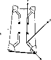
What Fig. 1 showed is the printed microstrip dual monopole antenna device of prior art, comprises the base of dielectric 1 of FR4 PCB form; Be positioned at the leading face 2 electrical ground of base of dielectric 1 downside; Printed microstrip line 3, this microstrip line 3 ends at two radiant sections 4; With the little T type section 5 of ground plane, the position of little T type section 5 between two radiants 4 of substrate 1 downside.
Fig. 1 has also shown the said equipment with section form, can find out that therefrom how two microstrip lines 3 are penetrated into its downside from the upside of substrate 1 by pair of slits in the ground plane 2 or hole 6, and ending at a pair of SMA connector 7, SMA connector 7 is by insulating washer 8 and ground plane 2 electric insulations.
Two microstrip lines 3 are configured to make radiant section 4 to point to the turning 9 of substrate 1, and are provided with 90 degree mutually.There is not ground plane 2 below the radiant section 4.
The antenna equipment of the prior art has narrow bandwidth in operation, because this reason, those skilled in the art recognizes that it is not suitable for mobile communication.
Fig. 2 has shown the antenna equipment of another prior art, be also included within its bottom side have conductive earthing face 2 and thereon side have the base of dielectric 1 of printed microstrip line 10.Printed microstrip line 10 stops in " fat " section 11 wideer significantly than the principal piece of printed microstrip line 10, thereby limits radiant section 11.Downside at radiant section 11 is not provided with ground plane 2.The edge 12 of ground plane 2 is as the ground plane of radiant section 11.This antenna equipment has good bandwidth, but antenna diversity is not provided.
Fig. 3 has shown first preferred embodiment of the present invention, comprises the base of dielectric 1 of FR4 or Duroid PCB form.The downside of base of dielectric 1 is provided with conductive earthing face 2 by metalized or other suitable processing.Conductive earthing face 2 extends to the edge of substrate 1, but does not extend into turning 9.In this embodiment, can find out that ground plane 2 has common hexagonal shape.Four feeder lines 13 extend to corner region 9 by the upper surface of substrate 1 from distributing point 14.Feeder line 13 is arranged at the middle body (although sometimes preferably feeder line 13 be arranged in the middle body of substrate 1 to be in 90 degree) of the upper surface of substrate 1 with the configuration mode that is parallel to each other, and then forward corner region 9 to, thereby make the end segment 15 of feeder line 13 be provided with in mutual rectangular mode.From Fig. 3, do not see the connector of substrate 1 downside, it provide with Fig. 1 in the mode of prior art unit affinity realize providing and being connected of distributing point 14 from the downside of substrate 1.The ceramic dielectric element 16 of wedge shape is soldered in the end segment 15 of each feeder line 13, and the sharp comer edge 17 of each element 16 is from its corner region 9 directed outwards separately simultaneously.When appropriate signals was imported into distributing point 14, the end segment 15 of dielectric device 16 and feeder line 13 was served as broadband (wideband) antenna together.In the application's context, each end segment 15 and relevant dielectric device 16 thereof define radiant.Should be noted that ground plane 2 extends to the marginal portion between the radiant of substrate 1 at the downside of substrate 1, help to isolate radiant like this.
Fig. 4 (being marked by the line of " not having ball ") has shown the S of one of four end segment 15 before using dielectric ceramic component 16
11Return loss.The antenna gain of being determined by this single end segment 15 is about 1dBi.When adding a small pieces dielectric ceramic material, produce the 2nd S
11Profile (profile) (being marked by the line of " bead "), the 2nd S
11Profile has shown the bandwidth that increases and up to the gain of 3dBi.Large stretch of ceramic component produces Three S's
11Profile (being marked by the line of " big ball ") also produces the postiive gain of crossing over very large bandwidth.Although echo consume is a spot of at the frequency place near 2200MHz, in the scope of-bandwidth that the 6dB level records from 1700MHz to surpassing 3GHz.What show in Fig. 3 is the antenna with more large stretch of ceramic component 16.
Owing to have ceramic component 16 (that is, the direction of leaving ground plane 2 is pointed at the turning 17 of the element 16 at 9 places, turning of substrate) in the position that Fig. 3 shows, in contiguous turning 9, increase by second ceramic component 16 and make some off resonance of antenna of winning.This behavior and antenna are the unities of thinking of dielectric load monopole or DLA.If element 16 moves to cover ground plane 2 towards ground plane 2, then antenna is not just worked.
If element 16 is rotated as shown in Figure 5 and is provided with, second element 16 can not make the first antenna off resonance in the contiguous turning 9, and therefore, above-mentioned antenna shows as high dielectric electric wire (HDA) rather than operates as dielectric load monopole.In this embodiment, allow element 16 to cover ground plane 2, this also is in fact desired.Should be realized that the antenna equipment that the present invention replaces embodiment can obtain by three dielectric devices that are equal to 16 further are set in the turning 9 of the part-structure shown in Fig. 5.
Fig. 6 has shown the embodiment (showing in stack mode in the figure) of the Fig. 3 with cartesian coordinate system.The z axle from substrate 1 vertically upward, x and y axle are arranged in the plane of substrate 1.
Fig. 7 to 12 has shown the radiation pattern of one of antenna of the equipment among Fig. 6 (that is, radiant section 15 and dielectric device 16) at 1900MHz, 1967MHz, 2034MHz, 2101MHz and 2168MHz frequency place with reference to the coordinate system among Fig. 6.
Specifically, Fig. 7 has shown the radiation pattern of xz plane copolar, Fig. 8 has shown the radiation pattern of yz plane copolar, Fig. 9 has shown the radiation pattern of xy plane copolar, Figure 10 has shown the radiation pattern of xz crossing on the same level polarization, Figure 11 has shown the radiation pattern of yz crossing on the same level polarization, and Figure 12 has shown the radiation pattern of xy crossing on the same level polarization.
Figure 13 has shown the antenna equipment among Fig. 3, and it has the indication of the 3-D cross correlation between the antenna ra-diation pattern of Fig. 7 to 12, and these cross correlations use Ansoft HFSS Electromagnetic Simulation packet to calculate.Cornerwise cross-correlation coefficient is 0.17, and the cross-correlation coefficient that strides across the width of substrate 1 is 0.001, and the cross-correlation coefficient that strides across the length of substrate 1 is 0.023.The embodiment that has 4 antennas among these numerals Fig. 3 has the good potential of setting up diversity in portable telephone device for example.
The diversity of antenna can be set up by polarization diversity, space diversity or pattern/directional diversity.The low cross correlation numeral that shows in Figure 13 causes mainly due to polarization diversity, but different electric wave directions has also played effect.Have been found that direction diversity can improve by the position of the dielectric device 16 in the manipulation base of dielectric 1 with by the element 16 of optimization substrate 1 downside and the slit between the ground plane 2 under the condition of sacrificing bandwidth.
Figure 14 has shown the embodiment of the beam pattern that is supposed to improve good direction diversity.In this configuration, the area of the ground plane 2 that each dielectric device 16 and radiant section 15 are removed below is less than the area of the ground plane of removing in the antenna that is used to measure curve in Fig. 7 to 12 2.Antenna equipment has good diversity and low front and back ratio, and wherein " back " direction is defined as the greatest irradiation direction with the similar antenna of back-to-back setting.(usually, be 180 degree between back lobe direction and the preceding lobe direction in same plane, that is, be passed down through the PCB substrate in this embodiment.Yet, in this article the back lobe of first antenna element is defined as identical more meaningfully with the direction of the preceding lobe of second antenna element, second antenna element and first antenna element back-to-back are provided with).Attention: have equipolarization, will have very different gains, low approximately in this embodiment 11dB rearwards rather than to the antenna of front (and therefore have about the vertical axis reflection pattern image).It is needed that this difference is used for the beam diversity set up between the antenna with equipolarization exactly.This antenna has the bandwidth that is about 200MHz, and is more much lower than the bandwidth of the antenna equipment that is used for Fig. 7 to 12.(be arranged in the turning 9 of substrate 1, as previously mentioned) isolation between changes from 7 to 15dB to have such four antennas of the radiation feature that shows in Figure 14.
In a word, given result demonstrates the corner that antenna is placed on mobile device and can set up antenna system (it has the impedance bandwidth of non-constant width and effectively has positive dBi gain for from 1.7 to 3GHz radiation pattern).Nearly four antenna can be installed among the PCB of mobile device.Above-mentioned antenna has low-down cross correlation, and this shows from this antenna system can obtain good diversity.
Figure 15 and 16 has shown the embodiment of alternative compactness of the present invention, and wherein, similar parts have identical label with the front embodiment.Feeder line 13 is in 90 degree ground configurations in the plane of substrate 1.In two radiant sections 15 and the relevant dielectric element 16 two are set in the adjacent corner regions 9 of base of dielectric.Yet, remaining two radiant section 15 ' and dielectric device 16 ' are set at the fringe region of substrate 1 rather than at corner region, simultaneously, below the radiant section 15 ' and dielectric device 16 ' of the upside of substrate 1, ground plane 2 is removed from the downside of substrate 1.In this mode, radiant section 15,15 ' is compared with the embodiment among Fig. 3 with dielectric device 16,16 ' and is flocked together more compactly, but the shape of ground plane 2 and being isolated mutually still by substrate 1 downside.The usefulness of this arrangement is that antenna element can tightly be accumulated in around the RF radio communication equipment (not shown), and the RF radio communication equipment will be between antenna element, and is usually located at the downside of substrate 1.By shortening the length of feeder line 13, can reduce the RF consume, although can produce the disadvantage that abuts against the increase electromagnetic coupled that causes together between the antenna owing to them.The feeder line of the embodiment among Figure 15 is shorter than the feeder line among Figure 16.Dielectric device 16,16 ' among Figure 15 and 16 is set in the substrate 1 so that dispose as HAD with radiant section 15,15 '.
Similar among the collating unit that Figure 17 shows and Figure 15 and 16 still has the oblong dielectric elements 16,16 ' that is welded in the low profile (low-profile) in the radiant section 15,15 '.
The concrete shape of the ground plane 2 of the embodiment among Figure 15 to 17 may be defined as " comet " shape.From having the rectangular ground plane of two longer sides and two shorter sides, from two longer edges, remove trapezoidal sections respectively, and remove the round corner section from each limit than the minor face edge.Utilize this mode, radiant is spaced from each other by the part of substrate, still leaves simultaneously enough ground planes and is used for various other control electronic device (not shown)s are installed in the PCB base.
Figure 18 to 21 has shown reflection and launching curve and the S that the quilt of each antenna a, b, c and d in the embodiment of Figure 17 records respectively
21Radiation pattern, and provide S for different antennae element a, b, c and d with this
11Impedance bandwidth and S
121The emission consume.
Figure 22 has shown the embodiment of second aspect of the present invention, and its parts identical with previous embodiments are denoted by the same reference numerals.This embodiment use with Figure 15 to 17 in identical " comet " shaped groundplane 2, but do not comprise dielectric device at radiant, locate not use " fat " monopole at radiant section 15,15 '.This can be counted as microstrip antenna (MSA).
Figure 23 has shown reflection and launching curve and the radiation pattern that is used at the antenna element of radiant section 15 definition at position a place, and can compare with the curve of the equivalent antenna of the dielectric device with Figure 17 shown in Figure 18.The antenna element of Figure 22 comes radiation with good bandwidth as can be seen, but begins and lower gain begins from higher frequency.
Figure 24 to 26 has shown three different antenna geometries, is denoted by the same reference numerals with parts identical in the previous embodiments.
Referring now to Figure 24, can find to be in two antennas (each all comprises radiant section 15 and dielectric device 16) that are provided with squarely by Computer Simulation and have-the reasonable isolation of 10.6dB and low cross-correlation coefficient 0.13, show that this device can perform well in diversity.
As shown in figure 25, when three antenna elements are placed to leg-of-mutton structure with the angle of the maximum possible between the plane of polarization (expectation provides best diversity), isolation effect is weak, for-5.3dB, cross-correlation coefficient is equally also very little, is 0.41.This is not a good layout for diversity.
At four antenna elements according to revolving the mode that turn 90 degrees each other when making up, as shown in figure 26.The poorest isolation (passing through diagonal) is also better, for-6.8dB, the poorest cross-correlation coefficient (still passing through diagonal) is also better, is 0.32.Cross-correlation coefficient between the element of sides adjacent is good especially, is 0.017.Obviously for diversity, this structure is extraordinary.
If use five elements, to compare with using three elements, it is bad that situation will become, and this is because the angle between plane of polarization only is 72 degree rather than 120 degree.
Like this, two or four elements brought in hand-held device, obtain diversity the best may because increased the selection of diversity, and realize that () possibility for example, Lucent BLAST method, four elements are preferred to the multiple-input and multiple-output communication technology.
Preferable feature of the present invention may be used on all aspects of the present invention, and can be with possible being used in combination arbitrarily.
In all specifications and claim, speech " comprises (comprise) " and the variation of " comprising " and this speech, for example " comprise (comprising) " and " comprising (comprises) " all refers to " including but not limited to ", be not to (not be) yet the assembly of getting rid of other, set, partly, additional or step.
Claims (18)
1. an antenna equipment comprises base of dielectric, has the first surface on top and the second surface of bottom; The conductive earthing face is on the described second surface or between described first and second surfaces; At least two electrically-conductive feed lines, be formed at described first surface, and extend to the edge that is positioned at described first surface or the predetermined radiant of corner part from distributing point, wherein, described ground plane does not extend below described radiant, it is characterized in that described ground plane is configured to extend between described radiant, described feeder line is broadened at described radiant place and/or is provided with discrete dielectric device at described radiant place.
2. equipment as claimed in claim 1, wherein, described feeder line is a microstrip feed line.
3. equipment as claimed in claim 1 or 2 wherein, is provided with four feeder lines and therefore four radiants is arranged in described first substrate.
4. equipment as claimed in claim 3, wherein, described substrate is generally the rectangular shape with four corner parts and four marginal portions, and each feeder line extends to corner part separately.
5. equipment as claimed in claim 3, wherein, described substrate is the common rectangular shape with four corner parts and four marginal portions, two feeder lines extend to adjacent corner part respectively, also have two feeder lines to extend to the opposed edges part respectively, in each in the described opposed edges part and the described adjacent corner part is adjacent.
6. equipment as claimed in claim 1 or 2 wherein, is provided with two feeder lines and therefore two radiants is arranged in described first surface.
7. equipment as claimed in claim 6, wherein, described two feeder lines extend to two adjacent corner parts of described first surface.
8. the described equipment of each claim as described above, wherein, described feeder line is set at adjacent radiant place, and meets at right angles each other.
9. as be subordinated to the described equipment of each claim of claim 3, wherein, described feeder line according to can by in pairs rather than the mode that individually drives be electrically connected to drive circuit.
10. the described equipment of each claim as described above, wherein, described feeder line is broadened at described radiant place, and be configured to have rectangle, taper shape, circle, ellipse, annular or polygonal shape.
11. as each described equipment in the claim 1 to 9, wherein, described feeder line is provided with dielectric ceramic component at described radiant place.
12. equipment as claimed in claim 11, wherein, described ceramic component is soldered to described feeder line at described radiant place.
13. as claim 11 or 12 described equipment, wherein, on described ceramic component and the surface that described feeder line contacts through metal treatment.
14. as each described equipment in the claim 11 to 14, wherein, the cylinder that being shaped as of described ceramic component has cusp edge and rounded edge fan-shaped.
15. equipment as claimed in claim 14, wherein, described ceramic component is arranged on the described first surface in the mode of the common directed outward of described cusp edge.
16. equipment as claimed in claim 14, wherein, described ceramic component is arranged on the described first surface in the mode that described cusp edge points to inner face jointly.
17. as each the described equipment in the claim 11 to 14, wherein, described ceramic component is a rectangle, and aligns with described feeder line at described radiant.
18. an antenna equipment comprises base of dielectric, has the first surface on top and the second surface of bottom; The conductive earthing face is on the described second surface or between described first and second surfaces; Four electrically-conductive feed lines, be formed at described first surface, and extend to predetermined radiant from distributing point, described predetermined radiant is positioned at the edge or the corner part of described first surface, wherein, described ground plane do not extend to described radiant below, it is characterized in that, described ground plane is configured to extend between described radiant, two adjacent corner parts that are positioned at described first surface in the described radiant also have two described radiants to be positioned at the marginal portion that faces one another of described first surface.
Applications Claiming Priority (2)
| Application Number | Priority Date | Filing Date | Title |
|---|---|---|---|
| GB0302818.0 | 2003-02-07 | ||
| GBGB0302818.0A GB0302818D0 (en) | 2003-02-07 | 2003-02-07 | Multiple antenna diversity on mobile telephone handsets, PDAs and other electrically small radio platforms |
Publications (1)
| Publication Number | Publication Date |
|---|---|
| CN1748339A true CN1748339A (en) | 2006-03-15 |
Family
ID=9952613
Family Applications (1)
| Application Number | Title | Priority Date | Filing Date |
|---|---|---|---|
| CN200480003756.6A Pending CN1748339A (en) | 2003-02-07 | 2004-02-09 | Multiple antenna diversity on mobile telephone handsets, pdas and other electrically small radio platforms |
Country Status (7)
| Country | Link |
|---|---|
| US (1) | US7245259B2 (en) |
| EP (2) | EP1590855A1 (en) |
| JP (1) | JP2006517074A (en) |
| KR (1) | KR20050098896A (en) |
| CN (1) | CN1748339A (en) |
| GB (2) | GB0302818D0 (en) |
| WO (1) | WO2004070874A1 (en) |
Cited By (4)
| Publication number | Priority date | Publication date | Assignee | Title |
|---|---|---|---|---|
| CN108777351A (en) * | 2018-04-18 | 2018-11-09 | 深圳市信维通信股份有限公司 | A kind of MIMO flat antenna systems and its mobile terminal for 5G communications |
| CN113016107A (en) * | 2018-06-27 | 2021-06-22 | 安费诺天线解决方案公司 | Four-port radiating element |
| CN113300105A (en) * | 2021-04-29 | 2021-08-24 | 郑州中科集成电路与信息系统产业创新研究院 | Ultra-wideband multiple-input multiple-output antenna with high isolation |
| TWI773508B (en) * | 2021-08-31 | 2022-08-01 | 川升股份有限公司 | Antenna module integrating polarization diversity and pattern diversity |
Families Citing this family (26)
| Publication number | Priority date | Publication date | Assignee | Title |
|---|---|---|---|---|
| ATE405966T1 (en) * | 2004-11-29 | 2008-09-15 | Sony Ericsson Mobile Comm Ab | PORTABLE COMMUNICATION DEVICE WITH WIDEBAND ANTENNA |
| GB0500856D0 (en) * | 2005-01-17 | 2005-02-23 | Antenova Ltd | Pure dielectric antennas and related devices |
| EP1880444A1 (en) | 2005-05-13 | 2008-01-23 | Fractus, S.A. | Antenna diversity system and slot antenna component |
| US7446714B2 (en) * | 2005-11-15 | 2008-11-04 | Clearone Communications, Inc. | Anti-reflective interference antennas with radially-oriented elements |
| TWI399886B (en) * | 2006-01-17 | 2013-06-21 | Antenova Ltd | Pure dielectric antennas and related devices |
| US8738103B2 (en) | 2006-07-18 | 2014-05-27 | Fractus, S.A. | Multiple-body-configuration multimedia and smartphone multifunction wireless devices |
| US20080030409A1 (en) * | 2006-08-03 | 2008-02-07 | Yih Lieh Shih | Rotational antenna apparatus for GPS device |
| JP4977048B2 (en) * | 2007-02-01 | 2012-07-18 | キヤノン株式会社 | Antenna element |
| WO2008114347A1 (en) * | 2007-03-16 | 2008-09-25 | Fujitsu Limited | Antenna arranging method and mounting device for communication device, and antenna device |
| KR100895448B1 (en) * | 2007-07-03 | 2009-05-07 | 삼성전자주식회사 | Miniatured Multiple-Input Multiple-Output Antenna |
| KR101484749B1 (en) * | 2008-08-19 | 2015-01-21 | 삼성전자주식회사 | An antenna apparatus |
| US7999749B2 (en) | 2008-10-23 | 2011-08-16 | Sony Ericsson Mobile Communications Ab | Antenna assembly |
| TWI381589B (en) * | 2008-10-30 | 2013-01-01 | Univ Nat Kaohsiung Marine | Planar monopole antennas for wlan multiple-input/multiple-output system |
| US8456377B2 (en) | 2009-11-04 | 2013-06-04 | Electronics And Telecommunications Research Institute | Method of disposing multiple antennas and communication apparatus using the method |
| TWI450442B (en) * | 2010-04-26 | 2014-08-21 | Quanta Comp Inc | A small multi-frequency antenna and a communication device using the antenna |
| FI20105656A0 (en) * | 2010-06-10 | 2010-06-10 | Valtion Teknillinen | Dielectric end load of an antenna |
| CN102104193B (en) * | 2010-12-01 | 2015-04-01 | 中兴通讯股份有限公司 | Multiple input multiple output antenna system |
| US9653813B2 (en) | 2011-05-13 | 2017-05-16 | Google Technology Holdings LLC | Diagonally-driven antenna system and method |
| TWI495197B (en) * | 2011-10-11 | 2015-08-01 | Univ Southern Taiwan | Monopole slot antenna of multiple-input and multiple-output with good isolation degree |
| US9711869B1 (en) * | 2013-03-07 | 2017-07-18 | Wichita State University | Hexaferrite slant and slot MIMO antenna element |
| TWI481117B (en) * | 2013-12-23 | 2015-04-11 | Wistron Neweb Corp | Antenna system |
| US10615499B2 (en) * | 2015-01-14 | 2020-04-07 | Skywave Mobile Communications Inc. | Dual role antenna assembly |
| US20160380681A1 (en) * | 2015-06-25 | 2016-12-29 | Qualcomm Incorporated | Simplified multi-band/carrier carrier aggregation radio frequency front-end based on frequency-shifted antennas |
| US9768506B2 (en) | 2015-09-15 | 2017-09-19 | Microsoft Technology Licensing, Llc | Multi-antennna isolation adjustment |
| CA3029398C (en) * | 2016-06-29 | 2024-02-20 | Dow Corning Toray Co., Ltd. | Silicone rubber composition and composite made therefrom |
| CN106654556B (en) * | 2016-12-16 | 2019-05-14 | 电子科技大学 | A kind of miniaturization broadband antenna suitable for 5G communication |
Family Cites Families (12)
| Publication number | Priority date | Publication date | Assignee | Title |
|---|---|---|---|---|
| US5453754A (en) * | 1992-07-02 | 1995-09-26 | The Secretary Of State For Defence In Her Brittanic Majesty's Government Of The United Kingdom Of Great Britain And Northern Ireland | Dielectric resonator antenna with wide bandwidth |
| CA2164669C (en) * | 1994-12-28 | 2000-01-18 | Martin Victor Schneider | Multi-branch miniature patch antenna having polarization and share diversity |
| CA2173679A1 (en) * | 1996-04-09 | 1997-10-10 | Apisak Ittipiboon | Broadband nonhomogeneous multi-segmented dielectric resonator antenna |
| KR100213373B1 (en) * | 1996-05-28 | 1999-08-02 | 이형도 | An antenna for wireless lan card |
| US6157344A (en) | 1999-02-05 | 2000-12-05 | Xertex Technologies, Inc. | Flat panel antenna |
| US6686886B2 (en) * | 2001-05-29 | 2004-02-03 | International Business Machines Corporation | Integrated antenna for laptop applications |
| US6549170B1 (en) | 2002-01-16 | 2003-04-15 | Accton Technology Corporation | Integrated dual-polarized printed monopole antenna |
| GB2386475A (en) * | 2002-03-12 | 2003-09-17 | Antenova Ltd | Multi-element dielectric resonator antenna |
| GB0207052D0 (en) * | 2002-03-26 | 2002-05-08 | Antenova Ltd | Novel dielectric resonator antenna resonance modes |
| US6624790B1 (en) | 2002-05-08 | 2003-09-23 | Accton Technology Corporation | Integrated dual-band printed monopole antenna |
| US6937193B2 (en) * | 2002-06-04 | 2005-08-30 | Skycross, Inc. | Wideband printed monopole antenna |
| FR2866480B1 (en) * | 2004-02-17 | 2006-07-28 | Cit Alcatel | MULTIPOLARIZED COMPACT RADIATION DEVICE WITH ORTHOGONAL POWER SUPPLY BY SURFACE FIELD LINE (S) |
-
2003
- 2003-02-07 GB GBGB0302818.0A patent/GB0302818D0/en not_active Ceased
-
2004
- 2004-02-09 KR KR1020057014488A patent/KR20050098896A/en not_active Application Discontinuation
- 2004-02-09 GB GB0402710A patent/GB2399683B/en not_active Expired - Fee Related
- 2004-02-09 CN CN200480003756.6A patent/CN1748339A/en active Pending
- 2004-02-09 EP EP04709284A patent/EP1590855A1/en not_active Withdrawn
- 2004-02-09 JP JP2006502256A patent/JP2006517074A/en active Pending
- 2004-02-09 US US10/544,478 patent/US7245259B2/en not_active Expired - Fee Related
- 2004-02-09 EP EP07103310A patent/EP1798811A1/en not_active Withdrawn
- 2004-02-09 WO PCT/GB2004/000511 patent/WO2004070874A1/en active Application Filing
Cited By (5)
| Publication number | Priority date | Publication date | Assignee | Title |
|---|---|---|---|---|
| CN108777351A (en) * | 2018-04-18 | 2018-11-09 | 深圳市信维通信股份有限公司 | A kind of MIMO flat antenna systems and its mobile terminal for 5G communications |
| CN108777351B (en) * | 2018-04-18 | 2023-10-17 | 深圳市信维通信股份有限公司 | MIMO planar antenna system for 5G communication and mobile terminal thereof |
| CN113016107A (en) * | 2018-06-27 | 2021-06-22 | 安费诺天线解决方案公司 | Four-port radiating element |
| CN113300105A (en) * | 2021-04-29 | 2021-08-24 | 郑州中科集成电路与信息系统产业创新研究院 | Ultra-wideband multiple-input multiple-output antenna with high isolation |
| TWI773508B (en) * | 2021-08-31 | 2022-08-01 | 川升股份有限公司 | Antenna module integrating polarization diversity and pattern diversity |
Also Published As
| Publication number | Publication date |
|---|---|
| EP1590855A1 (en) | 2005-11-02 |
| KR20050098896A (en) | 2005-10-12 |
| GB2399683A (en) | 2004-09-22 |
| GB0402710D0 (en) | 2004-03-10 |
| GB2399683B (en) | 2005-02-09 |
| US7245259B2 (en) | 2007-07-17 |
| WO2004070874A1 (en) | 2004-08-19 |
| GB0302818D0 (en) | 2003-03-12 |
| EP1798811A1 (en) | 2007-06-20 |
| US20060097919A1 (en) | 2006-05-11 |
| JP2006517074A (en) | 2006-07-13 |
Similar Documents
| Publication | Publication Date | Title |
|---|---|---|
| CN1748339A (en) | Multiple antenna diversity on mobile telephone handsets, pdas and other electrically small radio platforms | |
| CN105720361B (en) | A kind of broadband low section dual-polarization omnidirectional antenna based on Artificial magnetic conductor structure | |
| EP2887456B1 (en) | Antenna unit, antenna assembly, multi-antenna assembly, and wireless connection device | |
| CN109802231B (en) | Broadband electromagnetic dipole antenna based on artificial magnetic conductor | |
| US7705788B2 (en) | Multi-band antenna | |
| TWI509888B (en) | Directional antenna and smart antenna system using the same | |
| TW200411982A (en) | Wireless LAN antenna and wireless LAN card with the same | |
| US20080007465A1 (en) | Embedded multi-mode antenna architectures for wireless devices | |
| CN102800954B (en) | Antenna unit, antenna module and multi-antenna module | |
| GB2401994A (en) | Dual band antenna system with diversity | |
| CN105703084B (en) | A kind of room divided antenna | |
| CN207651657U (en) | A kind of circular polarisation omnidirectional antenna | |
| CN1234191C (en) | Bifrequency dipole antenna | |
| CN103887600A (en) | Wireless coverage antenna unit, antenna assembly and multi-antenna assembly | |
| KR100833175B1 (en) | Low profile omnidirectional antenna using magnetic loop current and Method thereof | |
| CN2924811Y (en) | Printed circuit board antenna | |
| CN2924818Y (en) | Planar three-frequency antenna | |
| KR100640339B1 (en) | Wideband monopole antenna | |
| You et al. | Highly efficient ultra-wideband planar folded dipole antenna for mobile applications | |
| CN103682604B (en) | Antenna element, multi-antenna component and radio interconnected equipment | |
| CN103594780B (en) | A kind of antenna | |
| CN201122655Y (en) | Miniature Bluetooth plane inverse F-shaped antenna | |
| JPH05259725A (en) | Diversity antenna for portable radio equipment | |
| KR20040004218A (en) | Wide band chip antenna for wireless LAN | |
| CN217881896U (en) | WiFi antenna with remote-location parasitic antenna and terminal |
Legal Events
| Date | Code | Title | Description |
|---|---|---|---|
| C06 | Publication | ||
| PB01 | Publication | ||
| C10 | Entry into substantive examination | ||
| SE01 | Entry into force of request for substantive examination | ||
| C02 | Deemed withdrawal of patent application after publication (patent law 2001) | ||
| WD01 | Invention patent application deemed withdrawn after publication |
Open date: 20060315 |