CN1701406A - Alkali metal generating agent, alkali metal generator, photoelectric surface, secondary electron emission surface, electron tube, method for manufacturing photoelectric surface, method for manufacturi - Google Patents
Alkali metal generating agent, alkali metal generator, photoelectric surface, secondary electron emission surface, electron tube, method for manufacturing photoelectric surface, method for manufacturi Download PDFInfo
- Publication number
- CN1701406A CN1701406A CNA2004800007698A CN200480000769A CN1701406A CN 1701406 A CN1701406 A CN 1701406A CN A2004800007698 A CNA2004800007698 A CN A2004800007698A CN 200480000769 A CN200480000769 A CN 200480000769A CN 1701406 A CN1701406 A CN 1701406A
- Authority
- CN
- China
- Prior art keywords
- alkali metal
- generating agent
- generator
- tube
- photoelectric
- Prior art date
- Legal status (The legal status is an assumption and is not a legal conclusion. Google has not performed a legal analysis and makes no representation as to the accuracy of the status listed.)
- Pending
Links
Images


Classifications
-
- C—CHEMISTRY; METALLURGY
- C22—METALLURGY; FERROUS OR NON-FERROUS ALLOYS; TREATMENT OF ALLOYS OR NON-FERROUS METALS
- C22B—PRODUCTION AND REFINING OF METALS; PRETREATMENT OF RAW MATERIALS
- C22B26/00—Obtaining alkali, alkaline earth metals or magnesium
- C22B26/10—Obtaining alkali metals
-
- C—CHEMISTRY; METALLURGY
- C22—METALLURGY; FERROUS OR NON-FERROUS ALLOYS; TREATMENT OF ALLOYS OR NON-FERROUS METALS
- C22B—PRODUCTION AND REFINING OF METALS; PRETREATMENT OF RAW MATERIALS
- C22B5/00—General methods of reducing to metals
- C22B5/02—Dry methods smelting of sulfides or formation of mattes
- C22B5/04—Dry methods smelting of sulfides or formation of mattes by aluminium, other metals or silicon
-
- C—CHEMISTRY; METALLURGY
- C23—COATING METALLIC MATERIAL; COATING MATERIAL WITH METALLIC MATERIAL; CHEMICAL SURFACE TREATMENT; DIFFUSION TREATMENT OF METALLIC MATERIAL; COATING BY VACUUM EVAPORATION, BY SPUTTERING, BY ION IMPLANTATION OR BY CHEMICAL VAPOUR DEPOSITION, IN GENERAL; INHIBITING CORROSION OF METALLIC MATERIAL OR INCRUSTATION IN GENERAL
- C23C—COATING METALLIC MATERIAL; COATING MATERIAL WITH METALLIC MATERIAL; SURFACE TREATMENT OF METALLIC MATERIAL BY DIFFUSION INTO THE SURFACE, BY CHEMICAL CONVERSION OR SUBSTITUTION; COATING BY VACUUM EVAPORATION, BY SPUTTERING, BY ION IMPLANTATION OR BY CHEMICAL VAPOUR DEPOSITION, IN GENERAL
- C23C14/00—Coating by vacuum evaporation, by sputtering or by ion implantation of the coating forming material
- C23C14/06—Coating by vacuum evaporation, by sputtering or by ion implantation of the coating forming material characterised by the coating material
- C23C14/14—Metallic material, boron or silicon
-
- C—CHEMISTRY; METALLURGY
- C23—COATING METALLIC MATERIAL; COATING MATERIAL WITH METALLIC MATERIAL; CHEMICAL SURFACE TREATMENT; DIFFUSION TREATMENT OF METALLIC MATERIAL; COATING BY VACUUM EVAPORATION, BY SPUTTERING, BY ION IMPLANTATION OR BY CHEMICAL VAPOUR DEPOSITION, IN GENERAL; INHIBITING CORROSION OF METALLIC MATERIAL OR INCRUSTATION IN GENERAL
- C23C—COATING METALLIC MATERIAL; COATING MATERIAL WITH METALLIC MATERIAL; SURFACE TREATMENT OF METALLIC MATERIAL BY DIFFUSION INTO THE SURFACE, BY CHEMICAL CONVERSION OR SUBSTITUTION; COATING BY VACUUM EVAPORATION, BY SPUTTERING, BY ION IMPLANTATION OR BY CHEMICAL VAPOUR DEPOSITION, IN GENERAL
- C23C14/00—Coating by vacuum evaporation, by sputtering or by ion implantation of the coating forming material
- C23C14/22—Coating by vacuum evaporation, by sputtering or by ion implantation of the coating forming material characterised by the process of coating
- C23C14/24—Vacuum evaporation
- C23C14/243—Crucibles for source material
-
- H—ELECTRICITY
- H01—ELECTRIC ELEMENTS
- H01J—ELECTRIC DISCHARGE TUBES OR DISCHARGE LAMPS
- H01J1/00—Details of electrodes, of magnetic control means, of screens, or of the mounting or spacing thereof, common to two or more basic types of discharge tubes or lamps
- H01J1/02—Main electrodes
- H01J1/35—Electrodes exhibiting both secondary emission and photo-emission
-
- H—ELECTRICITY
- H01—ELECTRIC ELEMENTS
- H01J—ELECTRIC DISCHARGE TUBES OR DISCHARGE LAMPS
- H01J9/00—Apparatus or processes specially adapted for the manufacture, installation, removal, maintenance of electric discharge tubes, discharge lamps, or parts thereof; Recovery of material from discharge tubes or lamps
- H01J9/02—Manufacture of electrodes or electrode systems
- H01J9/12—Manufacture of electrodes or electrode systems of photo-emissive cathodes; of secondary-emission electrodes
-
- H—ELECTRICITY
- H01—ELECTRIC ELEMENTS
- H01J—ELECTRIC DISCHARGE TUBES OR DISCHARGE LAMPS
- H01J2201/00—Electrodes common to discharge tubes
- H01J2201/32—Secondary emission electrodes
-
- H—ELECTRICITY
- H01—ELECTRIC ELEMENTS
- H01J—ELECTRIC DISCHARGE TUBES OR DISCHARGE LAMPS
- H01J2201/00—Electrodes common to discharge tubes
- H01J2201/34—Photoemissive electrodes
- H01J2201/342—Cathodes
- H01J2201/3421—Composition of the emitting surface
- H01J2201/3426—Alkaline metal compounds, e.g. Na-K-Sb
Landscapes
- Chemical & Material Sciences (AREA)
- Engineering & Computer Science (AREA)
- Organic Chemistry (AREA)
- Materials Engineering (AREA)
- Mechanical Engineering (AREA)
- Metallurgy (AREA)
- Manufacturing & Machinery (AREA)
- Chemical Kinetics & Catalysis (AREA)
- Life Sciences & Earth Sciences (AREA)
- Environmental & Geological Engineering (AREA)
- General Life Sciences & Earth Sciences (AREA)
- Geology (AREA)
- Common Detailed Techniques For Electron Tubes Or Discharge Tubes (AREA)
- Image-Pickup Tubes, Image-Amplification Tubes, And Storage Tubes (AREA)
Abstract
An alkali metal generating agent (1) for use in forming a photoelectric surface emitting a photoelectron corresponding to an incident light or a secondary electron emission surface emitting a secondary electron corresponding to an incident electron, which comprises an oxidizing agent comprising at least one molybdate having an alkali metal ion as a counter cation and a reducing agent for reducing the above cation. The above metal generating agent (1), which includes a molybdate having weaker oxidizing power than that of a chromate, undergoes slower oxidation-reduction reaction, which results in easier reaction rate control as compared to a conventional technique using a chromate, leading to the generation of an alkali metal with good stability.
Description
Technical Field
The present invention relates to an alkali metal generating agent, an alkali metal generator, a photoelectric surface, a secondary electron emission surface, an electron tube, a method for manufacturing the photoelectric surface, a method for manufacturing the secondary electron emission surface, and a method for manufacturing the electron tube.
Background
As is well known, photoelectric surfaces that emit electrons (photoelectrons, primary electrons) in response to incident light include a so-called transmissive photoelectric surface formed on a transparent substrate and a so-called reflective photoelectric surface formed on a metal substrate such as Ni, and such photoelectric surfaces are used as important components of electronic tubes such as photomultiplier tubes, photoelectric tubes, image intensifiers, and fast scanning tubes, for example.
The photoelectric element in practical use at present is often composed of a photoelectron emitting material (mainly, an intermetallic compound or a compound semiconductor) containing an alkali metal, forexample, an intermetallic compound composed of Sb and Cs, formed on a substrate.
At present, the vacuum is maintained at a predetermined degree of vacuum (preferably 10 in terms of partial pressure of residual gas)-7~10-2Pa) and temperature, and reacting the generated alkali metal vapor with a constituent material of the photoelectron emitting material that reacts with the alkali metal to form the photoelectron emitting material containing the alkali metal as a constituent element. For example, in a photoelectron emitting material for forming an intermetallic compound composed of Sb and Cs, a vapor deposited film composed of Sb, which is a constituent material of the photoelectron emitting material that reacts with an alkali metal, is formed on a substrate, and then Cs is reacted on the vapor deposited film composed of Sb by generating a vapor of Cs, thereby forming an intermetallic compound layer.
In this case, since the alkali metal is extremely unstable in the atmosphere and cannot itself serve as a generation source of the alkali metal vapor, a supply source (so-called alkali source or alkali metal source) containing a combination of an oxidizing agent and a reducing agent capable of generating the alkali metal by an oxidation-reduction reaction at a predetermined temperature as a constituent component is used. As such a supply source, for example, a powdery alkali metal source and an alkali metal source formed into a granular form under pressure are used. In this specification, the alkali metal source (supply source) of the alkali metal vapor containing the oxidizing agent and the reducing agent is referred to as an alkali metal generator.
Further, these powdery alkali metal generating agents or alkali metal generating agents formed into a granular form by pressurization are used in a state of being contained in a metal case having an opening through which an alkali metal vapor can be released to the outside. The metal case may be used in a state of being enclosed in a glass ampoule. The metal case is heated to generate an alkali metal vapor when the photoelectric surface is formed.
The alkali metal generating agent can be used for forming a secondary electron emission surface of a dynode in a photomultiplier tube, for example.
Currently, chromates (for example, Cs) containing an alkali metal ion as a counter cation and Si, Ti, Al or the like as a reducing agent are used as such alkali metal generating agents2CrO4) Alkali metal forming agents which are powdery or granulated under pressure as an oxidizing agent are disclosed in, for example, Japanese patent laid-open Nos. 55-78438, 53-124059, 45-7566 and 47-35221.
Disclosure of Invention
The inventors have found the following problems as a result of the above-described studies on the prior art. When an alkali metal generating agent containing a chromate having an alkali metal ion as a counter cation as an oxidizing agent is used to produce a photoelectric surface for the electron tube, the redox reaction between the oxidizing agent and the reducing agent using the chromate has a very high reaction rate, the temperature of the reaction field gradually increases, and the reaction rapidly proceeds after reaching a possible predetermined temperature.
More specifically, the temperature of the reaction field rapidly rises with the rapid progress of the redox reaction, and the alkali metal generating agent itself, or a metal case or a glass ampoule in which the alkali metal generating agent is stored may be broken. When such a case occurs in the production of an electro-optical surface in an electron tube, it is difficult to control the amount of alkali metal, and the desired performance cannot be obtained. In this case, the metal case after use is left in the case of an electron tube such as a glass container due to a manufacturing efficiency constraint, and the metal case is broken, which results in a product with a poor appearance.
Further, since the generation rate and yield of the alkali metal vary greatly due to rapid progress of the redox reaction, there is a problem that the deposition state of the alkali metal is not uniform in the region where the photoelectric surface should be formed and the secondary electron emission surface region where the dynode should be formed. For example, when the alkali metal generating agent is heated by a high-frequency heating method, since the oxidation-reduction reaction rapidly proceeds in the conventional chromate, the time for stopping heating cannot be generally fixed, and there are cases where dispersion occurs in spectral sensitivity characteristics (radiation sensitivity and quantum efficiency) between a plurality of photoelectric surfaces manufactured under the same conditions, or dispersion occurs in multiplication efficiency of a plurality of dynodes manufactured under the same conditions, resulting in a defective product and a reduction in production efficiency.
The present invention has been made to solve the above problems, and an object of the present invention is to provide an alkali metal generating agent for forming a photoelectric surface or a secondary electron emission surface capable of stably generating an alkali metal, an alkali metal generator containing the alkali metal generating agent and capable of easily controlling the generation rate of the alkali metal, a photoelectric surface having a sufficient spectral sensitivity characteristic, a secondary electron emission surface having a sufficient multiplication efficiency, and an electron tube having a sufficient photoelectric conversion characteristic. The present inventionalso aims to provide a method for manufacturing a photoelectric surface, a method for manufacturing a secondary electron emission surface, and a method for manufacturing an electron tube, which are easy to form and have excellent performance reproducibility.
The inventors have conducted extensive studies to achieve the above object and found that the conventional oxidation-reduction reaction between an oxidizing agent and a reducing agent has a high reaction rate, and that a chromate having a reducing agent, not the alkali metal ion of the oxidizing agent, as a counter cation has a very strong oxidizing ability, which is one of the main reasons.
The inventors have thus studied an oxidizing agent having a weaker oxidizing power than the chromate and found that when molybdate is used as such an oxidizing agent, a photoelectric surface and a secondary electron emission surface having similar performances to those of a photoelectric surface and a secondary electron emission surface which are currently manufactured using the chromate can be easily manufactured and have good reproducibility. As related techniques, there are WO02/093664, JP-B-48-20944, JP-B-47-21951, JP-B-47-25541 and JP-B-47-15976.
That is, the present invention is an alkali metal generating agent which is an alkali metal supply source used for forming a photoelectric surface for emitting photoelectrons in response to incident light or a secondary electron emission surface for emitting secondary electrons in response to incident light, and includes at least an oxidizing agent and a reducing agent. In particular, in the alkali metal generating agent, the oxidizing agent is composed of at least one molybdate salt having an alkali metal ion as a counter cation. The reducing agent starts a redox reaction with the oxidizing agent at a predetermined temperature to reduce the alkali metal ion.
Since molybdates having alkalimetal ions as the counter cation have a weaker oxidizing power than the above-mentioned chromates, the redox reaction with the reducing agent proceeds more slowly than in the case of chromates. Therefore, even when the reaction is started, the reaction rate can be easily controlled by adjusting the reaction temperature. In other words, the alkali metal generating agent of the present invention can stably generate an alkali metal (alkali metal vapor) without breaking itself or a case housing the agent.
Therefore, by using the alkali metal generating agent containing molybdate, a photoelectric surface having a sufficient spectral sensitivity characteristic and a secondary electron emission surface having a sufficient multiplication efficiency can be easily produced with good reproducibility.
The inventors have found that in producing a photoelectric surface having sufficient spectral characteristics and a secondary electron emission surface having sufficient multiplication efficiency, the mass ratio of the reducing agent to the molybdate is important. The inventors have made various samples (photomultiplier tubes) of the mass ratio of the reducing agent to the molybdate and studied the range in which a photocathode and an anode having sufficient sensitivity and stability can be obtained in practical use. As a result, it was found that the lower limit of the mass ratio of the reducing agent to the molybdate is 1.9 or more, preferably 4.0 or more. On the other hand, the upper limit of the mass ratio of the reducing agent to the molybdate is preferably 50.1 or less.
The alkali metal generator of this invention generates an alkali metal used in forming a photoelectric surface for releasing photoelectrons corresponding to incident light or a secondary electron release surface for releasing secondary electrons corresponding to incident electrons. The alkali metal generator has a housing,a supply source, and a discharge port. In particular, in the alkali metal generator, the housing is preferably a metal housing in which a supply source is incorporated. The supply source includes a raw material for generating an alkali metal and is an alkali metal generating agent having the above-described structure (the alkali metal generating agent of the present invention). The discharge port is provided in the housing, and discharges the alkali metal vapor generated in the supply source from the inner space of the housing in which the supply source is installed to the outside of the housing.
In the alkali metal generator of the present invention having the above-described structure and containing the alkali metal generating agent therein, the alkali metal (alkali metal vapor) generated by the redox reaction between the oxidizing agent and the reducing agent in the alkali metal generating agent can be stably released from the release port of the housing to the outside.
Therefore, by using the alkali metal generator of the present invention, a photoelectric surface having a sufficient spectral sensitivity characteristic and a secondary electron emission surface having a sufficient multiplication efficiency can be easily and reproducibly manufactured.
The photoelectric surface of the invention contains an alkali metal which releases photoelectrons corresponding to incident light. The alkali metal is an alkali metal generated from the alkali metal generating agent of the present invention. The alkali metal may be an alkali metal produced by the alkali metal generator of the present invention. In each case, a photoelectric surface having sufficient spectral sensitivity characteristics can be obtained by using the alkali metal generating agent or the alkali metal generator.
The secondary electron emission surface of the present invention contains an alkali metal which emits secondary electrons corresponding to incident electrons. The alkali metal may be an alkali metal produced from the alkali metal generating agent of the present invention, or may be an alkali metal produced from the alkali metal generating agent of the present invention. By using the alkali metal generating agent or the alkali metal generator in this manner, a secondary electron emission surface having a sufficient multiplication efficiency can be formed. The electrons incident on the secondary electron surface also include photoelectrons emitted from the photoelectric surface.
The electron tube of the present invention has a photoelectric surface for emitting photoelectrons in response to incident light, and the photoelectric surface of the present invention can be applied to the photoelectric surface.
By providing the photoelectric surface produced by the alkali metal generating agent or the alkali metal generator of the present invention in this manner, an electron tube having sufficient photoelectric conversion characteristics can be obtained. In the case where 1 or more secondary electron emission surfaces (for example, secondary electron emission surfaces of dynodes or the like) are provided in the electron tube, it is preferable that the secondary electron emission surfaces are also produced using the alkali metal generating agent or the alkali metal generator of the present invention from the above-described viewpoint.
The electron tube of the present invention includes at least an electron multiplier section including 1 or more dynodes having a secondary electron emission surface for emitting secondary electrons corresponding to incident electrons. In this case, the secondary electron emission surface of the present invention can also be applied as the secondary electron emission surface in each dynode.
By thus having the secondary electron emission surface manufactured by the alkali metal generating agent or the alkali metal generator of the present invention, an electron tube having sufficient photoelectric conversion characteristics can be obtained. In this case, the photoelectric surface provided in the electron tube is preferably produced by the alkali metal generating agent or the alkali metal generator of the present invention.
The method for producing a photovoltaic surface of the present invention comprises preparing the alkali metal generating agent or the alkali metal generator of the present invention as a source for generating an alkali metal, heating the alkali metal generating agent (in the case of the alkali metal generator, the alkali metal generating agent contained in the case), and then guiding the alkali metal generated by heating the alkali metal generating agent to a region where the photovoltaic surface is formed. Through the above steps, a photovoltaic surface containing an alkali metal that emits photoelectrons in response to incident light can be obtained.
Thus, by using the alkali metal generating agent of the present invention, a photovoltaic surface excellent in reproducibility of performance can be easily obtained.
The method for producing a secondary electron emission surface of the present invention comprises preparing the alkali metal generating agent or the alkali metal generator of the present invention as a source for generating an alkali metal, heating the alkali metal generating agent (in the case of the alkali metal generator, the alkali metal generating agent contained in the case), and then directing the alkali metal generated by heating the alkali metal generating agent to a region where the secondary electron emission surface is formed. This makes it possible to obtain a secondary electron emission surface that emits secondary electrons corresponding to the incident electrons.
Thus, by using the alkali metal generating agent of the present invention, a secondary electron emission surface having excellent reproducibility of performance can be easily obtained.
The electron tube manufacturing method of the present invention can manufacture an electron tube having at least a photoelectric surface containing an alkali metal which emits photoelectrons in response to incident light. That is, the method for producing the electron tube includes the steps of preparing the alkali metal generating agent or the alkali metal generator of the present invention, heating the alkali metal generating agent (in the case of the alkali metal generator, the alkali metal generating agent contained in the case), and then guiding the alkali metal generated by heating the alkali metal generating agent to the region where the photoelectric surface is formed.
By thus producing a photoelectric surface using the alkali metal generating agent or alkali metal generator of the present invention, an electron tube excellent in performance reproducibility can be obtained. In the case of producing an electron tube provided with at least 1 secondary electron emission surface (for example, a secondary electron emission surface such as a dynode) in addition to the photocathode, it is preferable that the secondary electron emission surface is also produced using the alkali metal generating agent or the alkali metal generator of the present invention from the above-mentioned viewpoint.
The electron tube manufacturing method of the present invention can manufacture an electron tube having an electron multiplying section including 1 or more dynodes having a secondary electron emission surface for emitting secondary electrons corresponding to incident electrons. In this case, the alkali metal generating agent or the alkali metal generator of the present invention is prepared, the alkali metal generating agent (in the case of the alkali metal generator, the alkali metal generating agent contained in the case) is heated, and then the alkali metal generated by heating the alkali metal generating agent is guided to the region where the secondary electron emission surface is formed, thereby obtaining the secondary electron emission surface in each dynode.
By thus producing the secondary electron emission surface of the dynode using the alkali metal generating agent or alkali metal generator of the present invention, an electron tube excellent in performance reproducibility can be obtained. In this case, from the above-mentioned viewpoint, the photoelectric surface of the electron tube is preferably also produced by using the alkali metal generating agent or alkali metal generator of the present invention.
Embodiments of the invention will be best understood from the following detailed description and accompanying drawings. These examples are merely illustrative and should not be construed as limiting the scope of the invention.
The scope of applicability of the present invention will become apparent from the detailed description given hereinafter. However, the detailed description and specific examples, while indicating embodiments of the invention suitable for use, are given by way of illustration only, since various changes and modifications within the spirit and scope of the invention will become apparent to those skilled in the art from this detailed description.
Drawings
FIG. 1 is a perspective view showing the structure of an embodiment of the alkali metal generating agent of the present invention.
Fig. 2 is a perspective view showing the structure of a first embodiment of the alkali metal generatorof the present invention.
Fig. 3 is a sectional view taken along line I-I of the alkali metal generator (fig. 2) of the first embodiment.
FIG. 4 is a sectional view showing the structure of a second embodiment of the alkali metal generator of the present invention.
FIG. 5 is a sectional view showing the structure of a third embodiment of the alkali metal generator of the present invention.
FIG. 6 is a sectional view showing the structure of a fourth embodiment of the alkali metal generator of the present invention.
FIG. 7 is a sectional view showing the structure of a fifth embodiment of the alkali metal generator of the present invention.
Fig. 8 is a diagram showing a photomultiplier tube structure as a first embodiment of the electron tube of this invention.
Fig. 9 is a diagram for explaining a process of manufacturing a photomultiplier tube and a dynode using the alkali metal generator shown in fig. 6.
Fig. 10 is a diagram showing a photomultiplier tube structure as a second embodiment of the electron tube of this invention.
Fig. 11 is a diagram showing a structure of a photoelectric tube as a third embodiment of the electron tube of this invention.
Fig. 12 is a diagram showing a structure of a moving image pickup tube (image intensifier) as a fourth embodiment of the electron tube of this invention.
Fig. 13 is a diagram showing a fast scan tube structure as a fifth embodiment of the electron tube of this invention.
Fig. 14 is a table showing characteristics (average values) of a sample of a photomultiplier tube produced using the alkali metal generating agent of the present invention and a comparative exampleof a photomultiplier tube produced using a conventional alkali metal generating agent.
Fig. 15 is a table showing Life characteristics (%) in samples of a photomultiplier tube produced using the alkali metal generating agent of the present invention and in comparative examples of a photomultiplier tube produced using a conventional alkali metal generating agent.
FIG. 16 is a graph showing the radiation sensitivity characteristics in a sample of a photomultiplier tube produced using the alkali metal generating agent of the present invention and a comparative example of a photomultiplier tube produced using a conventional alkali metal generating agent.
Fig. 17 is a graph showing relative outputs of Life (Life) characteristics of a photomultiplier tube manufactured using the conventional alkali metal generating agent, based on Life characteristics of a sample of the photomultiplier tube manufactured using the alkali metal generating agent of the present invention.
FIG. 18 is a graph showing the relative sensitivity of the photoelectric surface of a sample of a photomultiplier tube produced using the alkali metal generating agent of the present invention.
FIG. 19 is a graph showing the relative sensitivity of the anode in a sample of a photomultiplier tube produced using the alkali metal generating agent of the present invention.
Detailed Description
Examples of the alkali metal generating agent and the like of the present invention will be described in detail below with reference to FIGS. 1 to 19. In the description of the drawings, the same or corresponding portions are denoted by the same reference numerals, and redundant description is omitted.
(alkali Metal generating agent)
FIG. 1 is a perspective view showing the structure of an embodiment of the alkali metal generating agent of the present invention.
As described above, the alkali metal generating agent 1 shown in fig. 1 is an alkali metal supply source used for forming a photoelectric surface or a secondary electron emission surface. The alkali metal generating agent 1 of FIG. 1 is formed into cylindrical pellets from all the constituents by compression molding. The use properties of the alkali metal generating agent 1 are improved by the particles, and handling in the production of a photovoltaic surface, a secondary electron emission surface, and an electron tube is facilitated when the particles are incorporated into an alkali metal generator, which will be described later.
The oxidizing agent contained in the alkali metal generating agent 1 is composed of at least one molybdate having an alkali metal ion as a counter cation. As such molybdates, preference is given to using the formula R2MoO4Molybdate salt shown. R in the formula represents at least one metal element selected from Na, K, Rb and Cs.
By using a molybdate (hereinafter referred to as "molybdate") represented by R in the above chemical formula and having an alkali metal cation as a counter cation as an oxidizing agent, an alkali metal used for a practical photovoltaic material can be produced more stably. The kind and various contents of the oxidizing agent composed of molybdate are appropriately selected in accordance with the composition of the photoelectric element to be produced or the secondary electron emission element to be produced. For example, different kinds of materials may be combined and contained in a predetermined ratio, or may be contained alone.
The reducing agent contained in the alkali metal generator 1 starts a redox reaction with the oxidizing agent at a predetermined temperature to reduce the alkali metal ions. The reducing agent is not particularly limited as long as it can stably produce an alkali metal, but is preferably at least one selected from Si, Zr, Ti and Al. The alkali metal can be more stably generated by using Si, Zr, Ti and Al as reducing agents (for example, using a mixture of Si and Ti as a reducing agent) alone or in combination with the above-mentioned oxidizing agent composed of a molybdate.
The reducing agent composed of Si has a characteristic that the amount of alkali metal generated is saturated at about 900 ℃. Therefore, the amount of alkali metal produced can be controlled more easily at a heating temperature than at other reducing agents. Therefore, the reaction is easy in a short time, and is suitable for mass production. In addition, when Si is used as a reducing agent, a high-frequency heating reaction system in which it is difficult to control the temperature precisely can be used.
As a method for starting the redox reaction between the reducing agent and the oxidizing agent, there is a method of heating the alkali metal generating agent to a predetermined temperature at which the redox reaction starts in an atmosphere adjusted to a predetermined degree of vacuum. The term "atmosphere adjusted to a predetermined degree of vacuum" means 10 in terms of partial pressure of residual gas in the atmosphere-6~10-1Pa, preferably 10-6~10-3Pa atmosphere.
In addition, the alkali metal generating agent 1 may contain W, Al as a component other than the oxidizing agent and the reducing agent2O3And the like.
An example of the method for producing the alkali metal generating agent 1 will be described below. The alkali metal generating agent 1 can be produced by the same technique as that of the conventional alkali metal generating agent using chromate as the oxidizing agent, except that the molybdate is used as the oxidizing agent.
That is, molybdate which is an oxidizing agent having a composition corresponding to the composition of the produced photocathode or secondary electron emission surface of the dynode is selected.
Then, the measurement step, the pulverization-mixing step, and the molding step are sequentially performed. In this metering step, the oxidizing agent and the reducing agent (e.g., Si, Zr, Al, etc.) are metered in appropriate amounts. In the pulverizing-mixing step, they are charged into a pulverizer (e.g., an agate bowl, a ball mill, etc.), and pulverized and mixed at the same time. In the case where a component other than the oxidizing agent and the reducing agent is contained, in this pulverization-mixing step, the component is charged into a pulverizer together with the oxidizing agent and the reducing agent, and is mixed and pulverized to obtain an alkali metal generator powder. In the molding step, the obtained alkali metal generating agent powder is pressed with a powder pressing machine to obtain the alkali metal generating agent 1 molded into cylindrical particles.
In the above-mentioned forming step, the alkali metal generator is formed into cylindrical particles by compression. However, when the alkali metal generating agent of the present invention is compression molded, its shape is not particularly limited. The alkali metal generating agent of the present invention may be compression molded as in the above-described examples, or all the components may be in the form of powder. For example, the powder before molding may be used as it is, or may be used after being temporarily molded into particles and then pulverized into powder.
(alkali Metal Generator)
Suitable examples of the alkali metal generator of the present invention will be described below. Fig. 2 is a perspective view showing the structure of a first embodiment of the alkali metal generator of the present invention. FIG. 3 is a sectional view taken along line I-I of the alkali metal generator (FIG. 2) of the first embodiment, in which heating means are also shown.
The alkali metal generator 2 shown in fig. 2 and 3 generates an alkali metal used for forming a photoelectric surface or a secondary electron emission surface. The alkali metal generator 2 includes an alkali metal generating agent 1 shown in fig. 1 and a metal case 20 containing the alkali metal generating agent 1.
The case 20 has a metallic bottomed container 22 provided with a concave portion for storing the particles of the alkali metal generating agent 1, and a metallic lid member 24 welded to the bottomed container 22 so as to cover the entire concave portion of the bottomed container 22. The concave portion of the bottomed container 22 has a larger volume than the particles of the alkali metal generating agent 1, and is preferably formed in a shape similar to the particles. An annular flange is provided around the recess of the bottomed container 22, and the flange is welded to the edge portion of the lid member 24.
A recess (space for containing the alkali metal generating agent 1) of the bottomed container 22 and a non-welded portion outside the bottomed container 22 are provided between a flange of the bottomed container 22 and an edge of the lid member 24, and the non-welded portion serves as a discharge port 23 for discharging an alkali metal vapor generated from the alkali metal generating agent 1 to a photoelectric surface formation site or a secondary electron emission surface formation site of the dynode.
As a method for starting the oxidation-reduction reaction of the alkali metal generating agent 1 contained in the alkali metal generator 2, there is a method of heating the alkali metal generating agent 1 in an atmosphere adjusted to the predetermined degree of vacuum to a predetermined temperature at which the oxidation-reduction reaction starts.
More specifically, it is preferable to further include a heating device for generating the alkali metal vapor. Such a heating device is not particularly limited as long as it has a mechanism capable of heating the alkali metal generating agent 1 in the above atmosphere. For example, a high-frequency heating system or a resistance heating system may be used as the base. From the viewpoint of facilitating uniform heating of the alkali metal generating agent 1, the heating device preferably has a structure for heating the alkali metal generating agent 1 by a high-frequency heating system.
As shown in FIG. 3, the heating apparatus of the high-frequency heating system has a high-frequency coil 25 wound around a case 20 containing an alkali metal generating agent 1, and a high-frequency power supply for supplying a high-frequency current to the coil 25. For example, the same structure as that in the case where the alkali metal generating agent containing a conventional chromate as an oxidizing agent is heated by a high frequency heating method may be employed. For example, the alkali metal generating agent 1 may be fixed in advance in an electron tube in which a photoelectric surface and/or a secondary electron emission surface of a dynode is to be formed, and heated by a high-frequency heating system to generate an alkali metal vapor in the electron tube and react it at a predetermined portion where the photoelectric surface and/or the secondary electron emission surface of the dynode is to be formed.
In the method for producing the alkali metal generator 2, the alkali metal generator 1 is first produced as described above. Then, a bottomed container 22 and a lid member 24 are produced in conformity with the shape and volume of the alkali metal generating agent 1. The bottomed container 22 is welded to the lid member 24 in a state where the alkali metal generating agent 1 is contained in the recess. The method for producing the bottomed container 22 and the lid member 24 and the method for welding the bottomed container 22 and the lid member 24 are not particularly limited, and may be performed by a known technique, for example.
Although the case where the alkali metal generating agent 1 formed into particles is contained in the alkali metal generator 2 has been described, the alkali metal generator may be a powdered alkali metal generating agent before the alkali metal generating agent 1 is formed or a powdered alkali metal generating agent obtained by pulverizing the alkali metal generating agent 1, which is filled in the same casing 20 as the alkali metal generator 2.
Next, a second example of the alkali metal generator of the present invention will be described. FIG. 4 is a sectional view showing the structure of a second embodiment of the alkali metal generator of the present invention, in which a heating means is also shown. The alkali metal generator 3 shown in fig. 4 is composed of a main body 2A having the same structure as the alkali metal generator 2 shown in fig. 2 and 3, a glass ampoule 32 sealed in the main body 2A, and a rod-like support member 34 connected to the case 20 (having the discharge port 23) of the main body 2A.
The glass ampoule 32 has a cylindrical shape, and an upper surface portion (hereinafter referred to as a tip portion) facing a bottom surface of the cylinder through which the support member 34 penetrates has a smaller inner diameter than other portions. The alkali metal generator 3 is connected to an electron tube on which a secondary electron emission surface of the photocathode and/or dynode is to be formed, when the secondary electron emission surface of the photocathode and/or dynode is formed. At this time, the space in the electron tube where the photoelectric surface and/or the secondary electron emission surface of the dynode is to be formed is connected to communicate with the space in the glass ampoule 32. That is, the glass ampoule 32 is unsealed when the photoelectric surface and/or the secondary electron emission surface is formed.
One end of the support member 34 located inside the glass ampoule 32 is connected to the outer surface of the lid member 24 of the housing 20, and the other end of the support member 34 extends to the outside of the ampoule through a through hole h32 provided in the glass ampoule 32. The support member 34 is closely fitted to the inner surface of the through hole h32 to make the interior of the ampoule 32 airtight.
For example, a high-frequency heating system heating apparatus is constituted by a high-frequency power source 26 capable of generating a high-frequency current and a coil 25 (induction furnace) connected thereto and capable of passing the high-frequency current. The coil 25 is disposed so as to surround the body 2A from the outside of the glass ampoule 32, and the alkali metal vapor can be generated from the alkali metal generator 3 by heating.
In the method of producing the alkali metal generator 3, the alkali metal generating agent 1 is first produced as described above, and the main body 2A is produced in the same manner as the alkali metal generator 2. After the support member 34 is welded to the body 2A, which is integrally connected to the support member 34, is sealed in the glass ampoule 32. The method of welding the main body 2A and the support member 34 and the method of sealing them in the glass ampoule 32 are not particularly limited, and may be performed by a known technique, for example.
A third example of the alkali metal generator of the present invention will be explained. FIG. 5 is a sectional view showing the structure of a third embodiment of the alkali metal generator of the present invention, and the heating means is also shown in this figure. The alkali metal generator 4 shown in fig. 5 is composed of an alkali metal generating agent 1A in a powder form or a granular form and a metal (e.g., Ni) case 20A in which the alkali metal generating agent 1A is incorporated. The alkali metal generating agent 1A has the same composition as the alkali metal generating agent 1 shown in fig. 1.
The case 20A is made of a metal pipe having an internal space in which the alkali metal generating agent 1 is filled. The edge portions of the case 20A having both ends open are riveted with a chisel or the like, for example, so that the alkali metal generator 1A does not leak from the internal space. However, the case 20A is provided at the edge where the case 20A is caulked with an untouched portion which communicates the internal space and the outside of the case 20A, and this untouched portion serves as a discharge port 23 for discharging the alkali metal vapor generated from the alkali metal generating agent 1A to a portion where the photoelectric surface or the secondary electron emission surface is formed. The size of the discharge opening 23 is adjusted to such an extent that the alkali metal generating agent 1A does not leak from the internal space.
In the case of this alkali metal generator 4, the alkali metal vapor can be generated by heating, as in the case of the alkali metal generators 2 and 3 described above. The heating device for heating the alkali metal generator 4 is, as shown in FIG. 5, provided with a high-frequency coil 25 wound around the casing 20 and a high-frequency power source 26 for supplying a high-frequency current to the coil 25.
In the above-described method for producing the alkali metal generator 4, the alkali metal generating agent 1A is first produced as described above, and the inside of the metal shell (metal tube) 20A is filled with the agent. Then, the alkali metal generator 4 is obtained by caulking the opening portions of both ends of the metal case 20A. The method of caulking the openings at both ends of the metal case 20A is not particularly limited, and may be performed by a known technique, for example.
A fourth example of the alkali metal generator of the present invention will be explained. FIG. 6 is a sectional view showing the structure of a fourth embodiment of the alkali metal generator of the present invention, and the heating means is also shown in the drawing. The alkali metal generator 5 shown in fig. 6 has a main body 4A having the same structure as the alkali metal generator 4 shown in fig. 5, and a glass ampoule 52 sealed in the main body 4A. The glass ampoule 52 has the same shape as the glass ampoule 32 shown in fig. 4. Further, the inner diameter of the front end portion facing the bottom surface of the glass ampoule 52 is adjusted to a size capable of enclosing the main body 4A inside.
This alkali metal generator 5 is also connected to the electron tube on which the secondary electron emission surface of the photocathode and/or dynode is to be formed, like the alkali metal generator 3 shown in fig. 4, at the time of forming the secondary electron emission surface of the photocathode and/or dynode. At this time, the space in the electron tube in which the photoelectric surface and/or the secondary electron emission surface of the dynode is formed communicates with the space in the glass ampoule 52.
The alkali metal generator 5 can generate alkali metal vapor by heating, as in the case of the alkali metal generators 2 to 4. As shown in fig. 6, the heating device that heats this alkali metal generator 4 has a high-frequency coil 25 wound around the housing 20 and a high-frequency power supply 26 that supplies a high-frequency current to this coil 25.
In the method of manufacturing the alkali metal generator 5, the alkali metal generating agent 1A is first manufactured as described above, and the main body 4A is manufactured as in the alkali metal generator 4. The body portion 4A is then sealed in the glass ampoule 52. The method of sealing the body portion 4A in the glass ampoule 52 is not particularly limited, and may be performed by a known technique, for example.
The fifth embodiment of the alkali metal generator of the present invention will be explained. FIG. 7 is a sectional view showing the structure of a fifth embodiment of the alkali metal generator according to the present invention (including a heating means). The alkali metal generator 6 shown in fig. 7 mainly includes an alkali metal generating agent 1B in powder form or formed into particles, a metal case 20B accommodating the alkali metal generating agent 1A, 2 electrodes 64 arranged at predetermined positions of the metal case 20B, and an energizing device 68 electrically connected to each of the 2 electrodes 64 and having a power source for passing a current from one electrode 64 to the other electrode 64.
This alkali metal generating agent 1B has the same composition as the alkali metal generating agent 1 shown in fig. 1. The case 20B has a metal tube 62 provided with an internal space for containing the alkali metal generating agent 1, and 2 metal cover members 63 for closing both end openings of the metal tube 62. And 2 electrodes 64 are connected to 2 metal cover members 63 one by one. Furthermore, the current supply devices 68 are electrically connected to the 2 electrodes 64 by way of the lines 66.
A discharge port 23 for communicating the internal space with the outside of the case 20B is provided on a side surface ofthe metal pipe 62. The alkali metal vapor generated from the alkali metal generating agent 1A can be discharged to the photoelectric surface or the secondary electron emission surface formation portion through the discharge port 23. The size of the discharge opening 23 is adjusted to such an extent that the alkali metal generating agent 1B does not leak from the internal space. The shape of the discharge opening 23 having a size of the above-mentioned degree is not particularly limited, and may be, for example, a slit shape.
In the case of the alkali metal generator 6, the alkali metal generating agent 1B can be heated by the energization device 68 based on a resistance heating method. For example, when a current of several amperes is applied to the metal case 20B, the alkali metal generating agent 1B is heated by joule heat generated in the metal case 20B, and an alkali metal vapor can be generated.
In the method for producing the alkali metal generator 6, first, the alkali metal generator 1B is produced by the same method as the alkali metal generator 1, and the metal pipe 62 is filled with the alkali metal generator 1B. Then, both ends of the metal pipe 62 are respectively closed by welding the cover members 63 to cover the entire opening. Further, electrodes 64 were connected to 2 lid members 63, and electrodes 64 were connected to energizing device 68, thereby obtaining alkali metal generator 6.
(photoelectric surface, secondary electron emission surface, and electron tube)
Suitable examples of the photoelectric surface, the secondary electron emission surface, and the electron tube of the present invention will be described below.
First, a first embodiment of the electron tube of the present invention will be explained. Fig. 8 is a diagram showing a photomultiplier tube structure of the first embodiment of the electron tube of this invention. The photomultiplier tube 7 shown in fig. 8 has a configuration of an end window type photomultiplier tube that is a transmission type photoelectric surface (more specifically, the electron multiplier section is a line focus type in the case of the photomultiplier tube 7 shown in fig. 8). The photomultiplier tube 7 mainly has a photoelectric surface C7, an electron multiplier D7 having dynodes D71 to D79 having a secondary electron surface FD7 for emitting secondary electrons E2 by the collision of the photoelectron E1 while making the photoelectron E1 emitted from the photoelectric surface C7 incident thereon, a focusing electrode E7 disposed between the photoelectric surface C7 and the electron multiplier D72 for focusing the photoelectron E1 emitted from the photoelectric surface C7 and introducing the focused photoelectron E1 into the electron multiplier D7, an anode a7 for collecting the multiplied secondary electrons E2 and extracting them as a current to the outside, and a cylindrical (e.g., cylindrical) glass side tube 72 (e.g., Kovar (UV) glass, etc., or a metal material such as Kovar (Kovar) metal or stainless steel may be used) for placing these electrodes, and a voltage applying section (voltage dividing circuit) for potential adjustment is connected to each electrode.
The photoelectric surface C7 is mainly composed of a substrate C71 (panel), and a layer C72 (hereinafter referred to as a photoelectron emitting material layer C72) formed on the substrate C71 and formed of a film-like photoelectron emitting material (for example, an intermetallic compound or a compound semiconductor) that emits photoelectrons e1 in accordance with incident light L1.
This photoelectric surface C7 is fixed to the opening portion 72a at one end of the side tube 72. That is, the substrate C71 (for example, a glass substrate) which can transmit light to be used is fusion-fixed to the one end opening 72a of the side tube 72 with its light receiving surface FC71 directed outward. A layer of a photoelectron emitting material C72 is formed on the inner surface (back surface) of the substrate C71 opposite to the light receiving surface FC 71.
The photoelectron emitting material layer C72 contains an alkali metal generated from one of the alkali metal generating agent and the alkali metal generator containing the same. The photoelectron emitting material layer C72 is an intermetallic compound (compound semiconductor) containing an alkali metal as a constituent material or a compound semiconductor subjected to activation treatment with an alkali metal. Examples thereof include Sb-Cs, Sb-Rb-Cs, Sb-K-Cs, Sb-Na-K, Sb-Na-K-Cs, GaAs (Cs), InGaAs (Cs), InP/InGaAsP (Cs), and InP/InGaAs (Cs). In the above examples, (Cs) in GaAs (Cs), for example, means GaAs obtained by activating GaAs with Cs. The same applies to (Cs) in the following InP/InGaAsP (Cs) and InP/InGaAs (Cs). Further, photoelectron emitting materials such as Cs-Te and Ag-O-Cs may be used.
A material constituting a photoelectron emitting material which reacts with antimony and an alkali metal such as a compound semiconductor is formed on the back surface of the substrate C71, and then the alkali metal vapor is reacted to obtain the photoelectron emitting material layer C72.
Further, a stopper plate 78 made of glass (e.g., kowa glass, UV glass, or the like, or a metal material such as kowa metal or stainless steel may be used) is fused and fixed to the other opening 72b of the side pipe 72. Thus, the side tube 72, the photoelectric surface C7, and the plug plate 78 constitute a sealed container.
The exhaust pipe 73 is fixed to the center of the plug plate 4. The exhaust pipe 73 is used for exhausting the inside of the sealed container by a vacuum pump after the completion of the assembly of the photomultiplier tube 7 to be in a vacuum state, and alsoserves as an introduction pipe for introducing an alkali metal vapor into the sealed container when the photoelectron emitting material layer C72 is formed.
The electron multiplier section D7 includes first to ninth dynodes D71 to D79 each having a plurality of plate-like dynodes. The first dynode D71 to the ninth dynode D79 each include a substrate and a layer of a film-like secondary electron emitting material disposed on the substrate and having a secondary electron emitting surface FD7 which emits secondary electrons e2 by incident photoelectrons e 1. The layer made of the secondary electron release material is hereinafter referred to as a secondary electron release material layer.
The first dynode D71 to the ninth dynode D79 are supported in the sealed container by stem leads 75 (made of kowa metal, for example) provided so as to penetrate the sealed container, and the tip ends of the stem leads 75 are electrically connected to the first dynode D71 to the ninth dynode D79, respectively. The sealed container is provided with lead holes for passing the base leads 75 therethrough, and the lead holes are filled with a small plate (made of kovar glass, for example) to be hermetically sealed, and the base leads 75 are fixed to the sealed container by the small plate. The stem lead wires 75 include leads for the first dynode D71 to the ninth dynode D79 and a lead for the anode a 7.
In the electron multiplier section D7, the secondary electron emitting material of the secondary electron emitting material layer of each electron multiplier electrode contains an alkali metal generated from either one of the alkali metal generating agent and the alkali metal generator containing the agent. The secondary electron emitting material in the secondary electron emitting material layer is not particularly limited as long as it is a material having an alkali metal as a constituent material or a material subjected to activation treatment with an alkali metal. For example, an intermetallic compound (compound semiconductor) of a certain alkali metal and Sb, and the like can be exemplified.
An anode a7 fixed to the stem lead 75 is disposed between the electron multiplier section D7 and the plug 78. Further, a focusing electrode E7 is disposed between the electron multiplier section D7 and the photoelectric surface C7. An opening for discharging the focused photoelectrons E1 to the electron multiplier section D7 is formed in the focusing electrode E7.
The other ends of the stem leads 75 connected to the first dynode D71 to the ninth dynode D79 and the anode a7 are electrically connected to the voltage applying unit, so that predetermined voltages are applied to the first dynode D71 to the ninth dynode D79 and the anode a7, the photoelectric surface C7 and the focusing electrode E7 are set to the same potential, and the first dynode D71 to the ninth dynode D79 and the anode a7 are set to a high potential in this order from the upper layer.
Therefore, the light L1 incident on the light receiving surface FC71 of the photoelectric surface C7 is converted into photoelectrons e1, and is emitted from the inner surface FC 72. The photoelectrons e1 enter the electron multiplier section D7, are multiplied in multiple stages by the first dynode D71 to the ninth dynode D79, enter the anode a7, and send electric current from the anode a 7.
Next, a method for manufacturing the electron multiplier tube 7 (a method for manufacturing a photoelectric surface suitable for the present invention, a method for manufacturing a secondary electron emission surface suitable for the present invention, and an embodiment of a method for manufacturing an electron tube suitable for the present invention) will be described. The method for producing the photomultiplier tube 7 is not particularly limited in terms of conditions and order except for forming the photoelectric surface C7 and the first dynode D71 to the ninth dynode D79 with the alkali metal generating agent or the alkali metal generator of the present invention, and can be produced by a known technique.
That is, the side tube 72 and the base plate C71 are first integrated by heating (or a glass bulb (glass bulb) in which the side tube and the base plate are integrated may be used). At this stage, the photoelectron emitting material layer C72 is not formed on the substrate C71 of the photoelectric surface C7 (in a state where alkali activation is not performed).
Then, the anode a7, the focusing electrode E7, and the electron multiplier section D7 are assembled to the stem lead 75 penetrating the stopper 78, and inserted from the opening 72b side of the side tube 72. At this stage, the secondary electron surface is not formed (not activated by alkali) on the substrate serving as the dynode in the electron multiplier section D7. Thereafter, the stopper plate 78 and the side tube 72 were integrated in the same manner as the base plate C71 to obtain a sealed container.
Next, an example of a case where the photoelectric surface C7 of the photomultiplier tube 7 and the first to ninth dynodes D71 to D79 are formed will be described with reference to the alkali metal generator 5 shown in fig. 6. Fig. 9 is a diagram for explaining a manufacturing process of forming the photoelectric surface C7 and the first to ninth dynodes D71 to D79 of the photomultiplier tube 7 using the alkali metal generator 5 shown in fig. 6. The detailed internal structure of the photomultiplier tube 7 is omitted in fig. 9.
First, a layer composed of a constituent material of the photoelectron emitting material layer C72 that reacts with an alkali metal was formed in advance on the substrate C71, and a layer composed of a constituent material of the secondary electron emitting material layer that reacts with an alkali metal was formed in advance on the respective substrates of the dynodes D7. For example, a vapor deposition source (a vapor deposition source composed of a constituent material of the photoelectron emitting material layer C72 made of a metal other than an alkali metal such as Sb or a constituent material of the secondary electron emitting material layer made of a metal other than an alkali metal) is previously loaded into the sealed container.
Then, the inside of the sealed container is maintained in a predetermined vacuum state by a vacuum pump (the total pressure of the residual gas in the sealed container is, for example, 10)-6~10-3Pa) is added. In such a vacuum state, the vapor deposition source is energized or heated at a high frequency to evaporate the vapor deposition material constituting the vapor deposition source. Thereafter, the sealed container was placed in an electric furnace or the like, and the vapor deposition material was deposited on each of the substrates C71 and dynode D7 while maintaining the temperature at a predetermined temperature. The vapor deposition substance may be previously vapor-deposited on each of the substrate C71 and the dynode D7 by using another vapor deposition device.
After vapor deposition, an opening is formed in the exhaust pipe 73, and the vapor deposition material in the exhaust pipe 73 is opened to the outside. Next, as shown in fig. 9, a bottomed glass tube 76 in which the alkali metal generator 5 having the tip of the ampoule 52 in an open state is disposed near the bottom is prepared, and the opening of the glass tube 76 and the opening of the exhaust pipe 73 are connected in an airtight state. A separate opening is provided in the side surface of the glass tube 76, and the glass tube 76 is connected to the opening of a glass tube 77 connected to a vacuum pump. Thereafter, the inside of the sealed container is maintained in a predetermined vacuum state (the total pressure of the residual gas in the sealed container is, for example, 10) by a vacuum pump through an exhaust pipe 73-6~10-3Pa)。
By the above-mentioned high-frequency heating methodThe heating device (2) heats the alkali metal generator (5) to perform an oxidation-reduction reaction between the oxidizing agent (molybdate) and the reducing agent of the alkali metal generating agent (1A) in the alkali metal generator (5) to generate alkali metal vapor. For example, Cs is used as the oxidizing agent2MoO4When Si is used as the reducing agent, an oxidation-reduction reaction represented by the following chemical reaction formula is performed to generate Cs vapor.
In this case, the oxidizing agent (molybdate) having an alkali metal ion as a counter cation has a weaker oxidizing power than the chromate having an alkali metal ion as a counter cation, and the redox reaction with the reducing agent proceeds more slowly than the chromate. Therefore, the alkali metal vapor can be stably generated without breaking the alkali metal generating agent 1A itself or the case 20A containing the agent.
In other words, the reaction temperature can be easily adjusted by the heating exhaust pipe 73 after the oxidation reaction is started by the high-frequency heating type heating apparatus. The Cs vapor is induced to the front end portion of the glass ampoule 52 where the Cs vapor or Cs liquid is collected. Then, the sealed container is partially charged into an electric furnace, and the inside of the electric furnace is maintained at a predetermined temperature (for example, 200 ℃). At this time, the alkali metal generator 5 is moved to the side of the sealed container, and the tip portion of the ampoule 52 of the alkali metal generator 5 is inserted into the sealed container.
Thus, the tip portion of the ampoule 52 is kept at a predetermined temperature in the electric furnace, and the alkali metal vapor such as Cs can be stably emitted from the tip portion. That is, the photocathode C7 and the first dynode D71 to the ninth dynode D79 having performances equivalent to those of conventional photocathodes and dynodes made of chromate can be easily manufactured with excellent reproducibility.
The alkali metal vapor such as Cs stably released from the tip portion of the glass ampoule 52 into the sealed container in this way reacts with the prototype layer for forming the photoelectron emitting material layer C72 by reacting with the alkali metal of the photoelectric surface C7 or the prototype layer for forming the secondary electron emitting material layer by reacting with the alkali metal of the first dynode D71 to the ninth dynode D79, thereby producing a photoelectron emitting material or a secondary electron emitting material. Thereby forming the photoelectron emitting material layer C72 having a sufficient spectral sensitivity characteristic or the secondary electron emitting surface FD7 having a sufficient multiplication efficiency.
Then, the front end of the alkali metal generator 5 is taken out of the sealed container, and after the front end is moved to the bottom side of the glass tube 76, the glass tube 76 is cut and separated from the exhaust pipe 73.
By repeating the above operations with each alkali metal generating agent, a photoelectron emitting material layer C72 having a predetermined chemical composition was formed on the substrate C71, and a secondary electron emitting material layer having a predetermined chemical composition was formed on the substrate of the dynode. After the last use of thealkali metal generator 5, the inside of the photomultiplier tube 7 is kept at a predetermined temperature, and the vacuum pump is operated to remove the residual gas in the photomultiplier tube 7 sufficiently, thereby removing the alkali metal physically adsorbed to the parts other than the photoelectron emitting material and the secondary electron emitting material in the photomultiplier tube 7 and the gas generated from another vapor deposition source. Thereafter, by sealing the opening portion of the exhaust pipe 73 in the sealed container, a photomultiplier tube having sufficient photoelectric conversion characteristics is obtained.
A second embodiment of the electron tube of the invention is explained below. Fig. 10 is a diagram showing a photomultiplier tube structure of a second embodiment of the electron tube of this invention. Fig. 10 shows another structure of the photomultiplier tube 7 shown in fig. 8.
The photomultiplier 7A shown in fig. 10 mainly includes an electrode portion 71, an alkali metal generator 2 fixed to the electrode portion 71, glass containers having substantially cylindrical outer shapes and incorporating the electrode portion 71 and the alkali metal generator 2, and stem leads 75A electrically connected to the electrodes of the electrode portion 71, respectively. The glass container is composed of a glass side wall 72A and a glass stopper plate 78A. The electrode portion 71 is composed of an electron multiplier unit including a photoelectric surface, a focusing electrode, a plurality of dynodes, and an anode, as in the photomultiplier tube 7 of fig. 8. The stem leads 75A are connected to a voltage applying unit, similarly to the photomultiplier tube 7 of fig. 8.
The alkali metal generator 2 has the same structure as the alkali metal generator shown in fig. 2 and 3. The alkali metal generator 2 is used for a photomultiplier electrode forming a photoelectric surface of the electrodeportion 71 and an electron multiplier. The alkali metal generator 2 is fixed to the electrode portion 71 by a wire. The number of alkali metal generators 2 in fig. 10 is 1, and a plurality of alkali metal generators 2 containing alkali metal generating agents 1 having different chemical compositions may be fixed to the electrode portion 71 depending on the chemical composition of the photoelectric surface to be formed or the chemical composition of the secondary electron emission surface of the dynode.
The photomultiplier tube 7A is a side window type photomultiplier tube having a reflection type photoelectric surface with a photoelectric surface formed on a metal substrate. Therefore, the cylindrical side tube 72A constituting the glass container has translucency to light to be used, and the photoelectric surface substrate disposed in the electrode portion 71 is made of a metal substrate such as Ni. The photomultiplier tube 7A has, for example, the same structure as a well-known side window type photomultiplier tube except that it is supported by the electrode portion 71 and the alkali metal generator 2 fixed to the electrode portion 71.
In the above-described method for manufacturing the photomultiplier tube 7A, first, the glass stopper plate 78A having the stem lead 75A and the electrode portion 71 fixed to the stem lead 75A is fixed to the opening of the cylindrical glass side tube 72A having one end closed at the bottom. The alkali metal generator 2 is also mounted on the electrode portion 71 at this time. Further, when the exhaust pipe 73A connected to the plug plate 78A is opened, the opening portion is connected to the suction port of the vacuum pump.
At this time, an intermetallic compound layer (e.g., antimony layer) for reacting with an alkali metal to form an intermetallic compound layer is formed in advance on the secondary electron emission surface on which the photocathode substrate and the dynode are formed.
In each of the above cases, the glass container is kept in a predetermined vacuum state by a vacuum pump. In this vacuum state, the heating device of the high-frequency heating method heats the alkali metal generator 2 or the vapor deposition source from the outside of the glass container. The photoelectron emitting material layer of the photoelectric surface and the secondary electron emitting material layer of the dynode are thus formed.
In the case of the photomultiplier tube 7A, the oxidation-reduction reaction between the oxidizing agent (molybdate) and the reducing agent, which have alkali metal ions as counter cations, proceeds more slowly than the chromate reaction by heating the alkali metal generator 2 with a high-frequency heating type heating device. Therefore, the alkali metal vapor can be stably generated without breaking the alkali metal generating agent 1 itself or the case 20 containing the agent. In addition, the appearance of the glass container is not damaged even if the housing 20 is left in the glass container.
When the oxidation reaction is started by the high-frequency heating type heating apparatus, the glass container is placed in an electric furnace maintained at a predetermined temperature, and the alkali metal vapor can be reacted stably at the photoelectric surface formation site or the secondary electron emission surface formation site by temperature control. The alkali metal vapor reacts with a prototype layer for forming a photoelectron emitting material layer by reacting with an alkali metal of the photoelectric surface or a prototype layer for forming a secondary electron emitting material layer by reacting with an alkali metal of the dynode to produce a photoelectron emitting material or a secondary electron emitting material. Thereby forming a photoelectric surface having a sufficient spectral sensitivity characteristic or a secondaryelectron emission surface having a sufficient multiplication efficiency.
After the formation of the photoelectric surface or the secondary electron emission surface, the vacuum pump is operated in a state where the inside of the photomultiplier tube 7A is kept at a predetermined temperature, whereby the residual gas inside the photomultiplier tube 7A is sufficiently removed. In this way, the alkali metal and the gas generated from another vapor deposition source physically adsorbed to the photoelectron emitting material or the secondary electron emitting surface in the photoelectron multiplier tube 7 are removed. Thereafter, by sealing the opening portion of the exhaust pipe 73A on the glass container, the photomultiplier tube 7A having sufficient photoelectric conversion characteristics is obtained.
In forming this photomultiplier tube 7A, the alkali metal generator 3 shown in fig. 4 or the alkali metal generator 5 shown in fig. 6 may be used instead of the alkali metal generator 2. In this case, the photomultiplier tube 7A is also manufactured in the same order as the photomultiplier tube 7 described above.
In the case of the electron tube having a photoelectron multiplier structure, at least one of the photoelectron emitting material layer of the photoelectron surface and the secondary electron emitting material layer of the dynode may be formed using an alkali metal vapor generated from the alkali metal generating agent of the present invention or the alkali metal generator incorporated therein. For example, as in the above-described embodiments (photomultiplier tube 7 and photomultiplier tube 7A), both the photocathode and dynode may be formed using an alkali metal vapor generated from the alkali metal generating agent of the present invention or the alkali metal generator incorporated therein. In addition, only one of the photoelectron emitting material layer of the photoelectric surface and the secondary electron emitting material layer of the dynode may be formed using an alkali metal vapor generated from the alkali metal generating agent of the present invention or an alkali metal generator incorporated therein. But the former is preferable in view of manufacturing efficiency.
In the electron tube of the present invention, as in the above-described examples (photomultiplier tube 7 and photomultiplier tube 7A), when the dynode is provided, the shape of the dynode is not particularly limited. For example, in the above-described embodiment, the case where the line focus type dynode is mounted as the dynode D7 is described, but a dynode having a box type, a venetian blind type, a mesh type, a metal tunnel dynode type, or the like may be used.
A third embodiment of the electron tube of the present invention will be explained. Fig. 11 is a diagram showing a structure of a photoelectric tube of a third embodiment of the electron tube of this invention.
The photoelectric tube 8 shown in fig. 11 has the same structure as that of the photomultiplier tube 7 shown in fig. 8 except that the focusing electrode E7 and the electron multiplier section D7 constituting the photomultiplier tube 7 are not provided. The photoelectric surface C7 of this photoelectric cell 8 can also be easily manufactured as the photoelectric surfaces of the above-described photomultiplier tubes 7 and 7A. With the obtained photoelectric cell 8, sufficient photoelectric conversion characteristics can be obtained. The glass container in this electron tube 8 is composed of a glass side tube 72, a photoelectric surface C7, and a glass stopper plate 78.
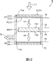
A fourth embodiment of the electron tube of the present invention will be explained. Fig. 12 is a diagram showing the structure of a moving image pickup tube (image intensifier) according to a fourth embodiment of the electron tube of the present invention.
The image intensifier 9 shown in fig. 12 has a photoelectric surface C7, a microchannel plate MCP for multiplying photoelectrons e1 emitted from the photoelectric surface C7, and a phosphor screen 90 for converting the electrons e2 emitted from the microchannel plate MCP into light. Furthermore, an exhaust pipe 72 is provided on the side pipe 72. In MCP, alkali activity due to an alkali metal generator does not proceed. Alternatively, the structure may be without MCP. The image pickup tube includes an X-ray image pickup tube for converting an X-ray image into a visible image.
In the case of the image intensifier 9 shown in fig. 12, the photoelectric surface C7 photoelectrically converts incident light L1 including optical two-dimensional information in the photoelectron emitting material layer C72 (for example, a photoelectric surface having a composition of GaAs — CsO or the like), and photoelectrons e1 corresponding to this incident light L1 are emitted from the inner surface FC 72. The voltage applying unit 74 for the microchannel plate MCP is held at a high potential with respect to the photoelectric surface C7, and when the photoelectron e1 enters, the secondary electron e2 is emitted by the collision of the photoelectron. An electron multiplication factor of several thousand to several ten thousand times can be obtained by applying a voltage of, for example, about 1000V between the incident surface F91 and the secondary electron emission surface F92 of the photoelectrons e1 of the microchannel plate MCP by a predetermined voltage applying unit.
The phosphor screen 90 is composed of a transparent substrate 94, a phosphor layer 92 formed on the transparent substrate 94, and an electrode 75 formed on the surface of the phosphor layer 92. This electrode 75 is an electrode for accelerating the multiplied secondary electron e2, and is used for applying a voltage adjusted to a predetermined potential. That is, this electrode 75 is also held at a high potential with respect to the voltage application part 74 of the secondary electron exit surface F92 of the microchannel plate MCP.
The constituent material of the phosphor layer 92 and the constituent material of the substrate 94 are not particularly limited, and well-known materials can be used. For example, an optical fiber plate formed by binding a plurality of optical fibers may be used as the substrate 94, and a metal thin film may be disposed between the optical fiber plate and the phosphor layer.
The photoelectric surface C7 of the image intensifier 9 is also similar to the photoelectric surface C7 of the photomultiplier tubes 7 and 7A described above, and can be easily manufactured. Sufficient photoelectric conversion characteristics can be obtained with respect to the obtained image intensifier 9.
A fifth embodiment of the electron tube of the present invention will be explained. Fig. 13 is a diagram showing a structure of a fast scan tube of a fifth embodiment of the electron tube of the present invention.
In the fast scanning tube 10 shown in fig. 13, the photoelectric surface C7 is disposed on the side of the one end opening 72a of the side tube 72, similarly to the photomultiplier tube 7 shown in fig. 8. Light to be measured L1 incident from the outside is converted into photoelectrons in the photoelectron emitting material layer C72 of the photoelectric surface C7.
Further, in the side tube 72, a flat plate-shaped accelerating electrode 11 for accelerating photoelectrons emitted from the inner surface FC72 is disposed in the vicinity of the photoelectric surface C7. The accelerating electrode 11 is disposed so that the normal line of the electrode surface and the normal line of the inner surface FC72 aresubstantially parallel to each other. A focusing electrode 12 for focusing the primary electrons accelerated by the accelerating electrode 11 is disposed in the vicinity of the accelerating electrode 11. The focusing electrode 12 is formed of a pair of flat plate-shaped electrodes, and the electrode surfaces are parallel to each other and arranged substantially perpendicular to the inner surface FC 72. Further, a communicating hole H10 through which the primary electrons focused by the focusing electrode 12 can pass is formed near the focusing electrode 12, and a disk-shaped anode a10 that collects the electrons and passes the electrons through inside the communicating hole H10 is disposed.
A deflection electrode 14 for scanning electrons passing through the anode a10 opening H10 at high speed is provided in the vicinity of the anode a 10. The deflection electrode 14 is constituted by 1 pair of plate-shaped electrodes arranged to face each other. The normals of the electrode surfaces of the pair of electrodes 1 are parallel to each other, and the normals are perpendicular to the normal of the inner surface FC 72. A predetermined deflection voltage is applied between 1 pair of flat plate electrodes, and thus primary electrons released from the anode a10 through the opening H10 are scanned in a predetermined direction.
In addition, a microchannel plate MCP for multiplying electrons scanned by the deflection electrode 14 is disposed in the vicinity of the deflection electrode 14. The fast scan tube 10 may be a structure without the microchannel plate MCP.
A phosphor screen 90 for converting electrons emitted from the microchannel plate MCP into light is provided in the vicinity of the microchannel plate MCP. This phosphor screen 90 has the same structure as the phosphor screen 90 shown in fig. 12. Thus, a sealed container is constituted by the panel C71, the transparent substrate 94, and the side tube 72.
In the fast scanning tube 10, when the test light L1 is made incident on the photoelectric surface C7 through the slit plate, the test light is converted into an electron image, accelerated by the accelerating electrode 11, and collected in the anode a 10. The electron image enters between 2 deflection electrodes 14 through an anode a10, and is scanned at high speed in a direction parallel to the normal direction of the electrode surface of the deflection electrode 14. The electrons are scanned at a high speed because the number of electrons passing through the deflection electrode 14 varies corresponding to a temporal change in light intensity of the test light that varies at a high speed with respect to time.
The electrons thus scanned at high speed are multiplied by the microchannel plate MCP, and the electrons multiplied by the microchannel plate MCP are converted into an optical image (also referred to as a fast scan image) on the phosphor screen 90. Thus the temporal variation of the intensity of the light to be tested is converted into a spatial variation of the light intensity in the phosphor screen 90. When the fast scanning tube is operated, electrons are scanned in synchronization with the passage timing, and the spatial change of the light intensity projected onto the phosphor electrode 90, that is, the temporal change thereof can be known by analyzing the fast scanning image.
The photosurface of the fast scan tube 10 is also as easy to manufacture as the photomultiplier tubes 7 and 7A described above. And sufficient photoelectric conversion characteristics can be obtained with respect to the obtained fast scanning tube 10.
(test)
The present invention will be described in more detail below by way of examples of the alkali metal generating agent of the present invention and comparative examples thereof. The present invention is not limited to these examples.
(sample)
The inventors produced a plurality of photomultiplier tubes (having the same structure as that of FIG. 10) having the same structure as that of a commercially available side-window type photomultiplier tube, except that each sample was equipped with a photocathode (antimony-cesium photocathode: Cs-Sb, substrate material Ni) formed by an alkali metal generating agent shown below and a secondary electron emission surface (Cs-Sb) formed by an alkali metal generating agent shown below. In the case of producing a double alkali photoelectric surface and a multiple alkali photoelectric surface containing a plurality of alkali metals, a plurality of molybdates and reducing agents may be contained in 1 alkali metal generator. Alternatively, a plurality of alkali metal generators may be prepared for each alkali metal by charging an alkali metal generator containing a molybdate and a reducing agent.
The alkali metal generator for forming the photoelectric surface contains molybdate (Cs) as an oxidizing agent2MoO4) And Si as a reducing agent. The alkali metal generating agent is in the form of granules as in fig. 1, and the mass ratio of the oxidizing agent to the reducing agent is 1: 2 (oxidizing agent: reducing agent).
This sample utilizes an alkali metal generating agent for forming a secondary electron emission surface and a photoelectric surface.
The above-mentioned metering step, the above-mentioned pulverization-mixing step and the above-mentioned molding step are sequentially carried out on the above-mentioned mixture of molybdates to obtain an alkali metal generating agent.
Then, samples of these alkali metal generating agents were put into the metal cases 20 shown in FIGS. 2 and 3, respectively, and the metal cases 20 were put into the glass ampule 32 as shown in FIG. 4, thereby producing an alkali metal generator having the same structure as the alkali metal generator 3.
A photoelectric surface and a secondary electron emission surface were produced by the same method as the method for producing the photomultiplier tube 7 described with reference to fig. 9, except that an alkali metal generator was used, to obtain a photomultiplier tube.
(comparative example)
On the other hand, the inventors produced, as a comparative example, a plurality of photomultiplier tubes having the same structure as that of a commercially available side window type photomultiplier tube by the same method as that of the above-described sample. In-suit clothesThe photoelectric surface incorporated in the photomultiplier of this comparative example was formed by using a solution containing chromate (Cs) as an oxidizing agent2Cro4) And Si as a reducing agent, and a conventional alkali metal generating agent (antimony cesium photoelectric surface: Cs-Sb).
(characteristic evaluation test)
The radiation sensitivity (mA/W), Life (%) (change of Sp with time) was also measured for each of the characteristics of the cathode output (Sk: μ A/lm), the anode output (Sp: μ A/lm), the dark current (Idb: nA) and the After Pulse (%) (for the photomultiplier tube of the above-produced sample and comparative example). Fig. 14 to 17 show tables and graphs showing the results of the detection. The above-mentioned properties were measured based on the methods described in "photomultiplier tube" and its base and application "(edited committee of creek photonics corporation) (for example, p.34 to 39:" basic properties of a photoelectric surface ", p.60 to 73:" properties of a photomultiplier tube ", and the like).
Fig. 14 is atable showing characteristics (average values) of a sample of a photomultiplier tube produced using the alkali metal generating agent of the present invention and a comparative example of a photomultiplier tube produced using a conventional alkali metal generating agent. Fig. 15 is a table showing Life characteristics (%) in samples of a photomultiplier tube produced using the alkali metal generating agent of the present invention and in comparative examples of a photomultiplier tube produced using a conventional alkali metal generating agent. FIG. 16 is a graph showing the radiation sensitivity characteristics in a sample of a photomultiplier tube produced using the alkali metal generating agent of the present invention and a comparative example of a photomultiplier tube produced using a conventional alkali metal generating agent. In this FIG. 16, a graph G1610 shows the results of detection of the photomultiplier tube of this sample, and a graph G1620 shows the results of detection of the photomultiplier tube of the comparative example. Fig. 17 is a graph showing the relative output of the Life characteristics of comparative examples of photomultiplier tubes manufactured using conventional alkali metal generators, based on the Life characteristics of the photomultiplier tube samples manufactured using the alkali metal generators of the present invention. In fig. 17, a curve P1 shows Life characteristics of the photomultiplier tube of this sample, and curves P2 to P4 show relative outputs of Life characteristics of the photomultiplier tube of the comparative example based on P1.
In particular, relative outputs P2 to P4 of Life characteristics of photomultiplier tubes (commercially available photomultiplier tubes) of the comparative example shown in fig. 17 were obtained by measuring data on a plurality of (35) samples. That is, the curve P2 represents the average of all data, the curve P3 represents the average + σ (σ is the standard deviation) of all data, and the curve P4represents the total- σ (σ is the standard deviation).
From the detection results shown in fig. 16, it was clearly confirmed that the sample produced as the photomultiplier of this invention had the same radiation sensitivity as the conventional photomultiplier of the comparative example.
It is clear from the table shown in fig. 15 that the photomultiplier of this sample has the same Life characteristics as the conventional photomultiplier of the comparative example. The Life characteristic evaluation test was carried out with the operating current (output current) of each photomultiplier tube set to 100. mu.A and the applied voltage between the photoelectric surface and the anode set to 1000V. The Life characteristic (relative output) value of the table shown in fig. 15 represents a relative value in which the value of the anode output (Sp) after 1 hour from the start of the detection is 100%.
As shown in fig. 17, it was confirmed that the photomultiplier tube sample of the present invention (the curve P1 showing the Life characteristics of the sample in fig. 17 is an average of 5 samples) can obtain a relative output showing Life characteristics substantially the same as those of the photomultiplier tube of the comparative example, and has excellent characteristic reproducibility.
As shown in the table of fig. 14, it was confirmed that the photomultiplier tube of this sample (the photomultiplier tube of the present invention) had the same cathode output, anode output, dark current, and After Pulse characteristics as those of the conventional photomultiplier tube. After Pulse characteristics were measured by using an LED (semiconductor laser), Pulse signals were output from each of the photomultiplier tubes of the sample and the comparative example, and the output signals were calculated based on After Pulse generated between 0.5 μ sec and 10 μ sec.
The inventors prepared a plurality of samples having different mass ratios of the reducing agent (Si) to the molybdate (i.e., reducing agent/Mo acid salt) for the photomultiplier tube produced using the alkali metal generating agent of the present invention, and examined the relative sensitivities of the photocathode and the anode at each mass ratio. FIG. 18 is a graph showing the relative sensitivity of the photoelectric surface of a sample of a photomultiplier tube produced using the alkali metal generating agent of the present invention. FIG. 19 is a graph showing the relative anode sensitivity of a sample of a photomultiplier tube produced using the alkali metal generating agent of the present invention. Fig. 18 and 19 show the maximum value (MAX.), the average value (AVE.), and the minimum value (MIN.) of the respective substance-to-substance ratios. The particle weights of the samples prepared as the alkali metal generating agent were 57mg for the sample with the mass ratio of 1.2, 59mg for the sample with the mass ratio of 1.6, 61mg for the sample with the mass ratio of 1.9, 71mg for the sample with the mass ratio of 4, 80mg for the sample with the mass ratio of 6.1, 109mg for the sample with the mass ratio of 12.1, 129mg for the sample with the mass ratio of 20.2, 148mg for the sample with the mass ratio of 28.3, 205mg for the sample with the mass ratio of 32.3, 290mg for the sample with the mass ratio of 50.1, and 382mg for the sample with the mass ratio of 69.5, respectively.
As can be seen from fig. 18, in order to obtain sufficient relative sensitivity (Sk) for the cathode (photoelectric surface) of the photomultiplier, the substance mass ratio (reducing agent/Mo acid salt) is preferably 1.9 or more. Further, in order to ensure higher stability of the photomultiplier tube (to reduce fluctuation in sensitivity between manufactured photomultiplier tubes), it is preferable that the mass ratio is 4.0or more. Theoretically, as can be seen from the above chemical reaction formula, the mass ratio of the reducing agent to the molybdate is 1.2. Therefore, the lower limit of the mass ratio of the reducing agent to the molybdate is 1.9 or more, preferably 4.0 or more. This mass ratio is important as described above due to the high level of technology that is available to create the photovoltaic surface such that the electron surface is released. On the other hand, in the case of 50.1 and 69.5, the obtained photomultiplier tube cannot be considered to be significantly inferior in sensitivity and stability. However, if the reducing agent is too much, it is difficult to control the heating time for obtaining the most suitable oxidation-reduction reaction (it is difficult to manufacture a photomultiplier tube equipped with a photoelectric surface having desired sensitivity and stability). In particular, when the heating method is a high-frequency heating method, stable reduction can be achieved. If the reducing agent is too much, it requires heating many times, making it difficult to determine the production technique and lowering the stability in mass production. In addition, when the photomultiplier is mass-produced, there is a possibility that the stability of the photomultiplier is lowered. Therefore, the upper limit of the mass ratio of the reducing agent to the molybdate, which affects the stability, is preferably 50.1 or less.
As can also be seen from fig. 19, in order to obtain sufficient relative sensitivity (Sp) for the anode of the photomultiplier, the mass ratio (═ reducing agent/Mo acid salt) is preferably 1.9 or more. For the same reason as in the case of the above-described photoelectric element, the upper limit of the substance ratio of the reducing agent to the molybdate is preferably 50.1 or less.
It will be apparent from the foregoing description of the invention that numerous variations of the invention are possible. Such variations are not to be regarded as a departure from the spirit and scope of the invention, and all such modifications as would be obvious to one skilled in the art are intended to be included within the scope of the following claims.
Possibility of industrial utilization
In the case of the present invention as described above, the reaction rate can be easily controlled by controlling the reaction temperature alone in the redox reaction between the oxidizing agent (molybdate) and the reducing agent using the alkali metal ion as the counter cation. Therefore, an alkali metal generating agent for forming a photoelectric surface or a secondary electron emission surface, which can stably generate an alkali metal at a predetermined temperature, can be provided. Further, an alkali metal generator having the alkali metal generating agent and capable of easily controlling the generation rate of an alkali metal can be provided.
Further, the alkali metal generating agent or the alkali metal generator of the present invention can provide a photoelectric surface having a sufficient spectral sensitivity characteristic, a secondary electron emission surface having a sufficient multiplication efficiency, and an electron tube having both a sufficient optical characteristic and an electrical characteristic.
Further, it is possible to provide a method for producing a photoelectric surface, a method for producing a secondary electron emission surface, and a method for producing an electron tube, which are easily formed by using the alkali metal generating agent or the alkali metal generator of the present invention and have excellent reproducibility of the obtained performance.
Claims (38)
1. An alkali metal generating agent as an alkali metal supply source used for forming a photoelectric surface for emitting photoelectrons in response to incident light or a secondary electron emission surface for emitting secondary electrons in response to incident electrons, the alkali metal generating agent comprising at least:
an oxidizing agent consisting of at least one molybdate salt having an alkali metal ion as the counter cation; and
a reducing agent which starts a redox reaction with the oxidizing agent at a predetermined temperature to reduce the alkali metal ion,
the mass ratio of the reducing agent to the molybdate is 1.9 to 50.1.
2. An alkali metal generating agent as an alkali metal supply source used for forming a photoelectric surface for emitting photoelectrons in response to incident light or a secondary electron emission surface for emitting secondary electrons in response to incident electrons, the alkali metal generating agent comprising at least:
an oxidizing agent consisting of at least one molybdate salt having an alkali metal ion as the counter cation; and
a reducing agent which starts a redox reaction with the oxidizing agent at a predetermined temperature to reduce the alkali metal ion,
the mass ratio of the reducing agent to the molybdate is 4.0 to 50.1.
3. An alkali metal generating agent as an alkali metal supply source used for forming a photoelectric surface for emitting photoelectrons in response to incident light or a secondary electron emission surface for emitting secondary electrons in response to incident electrons, the alkali metal generating agent comprising at least:
an oxidizing agent consisting of at least one molybdate salt having an alkali metal ion as the counter cation; and
a reducing agent composed of Si which starts a redox reaction with the oxidizing agent at a predetermined temperature and reduces the alkali metal ions.
4. An alkali metal generating agent as an alkali metal supply source containing at least Cs for use in forming a photoelectric surface for emitting photoelectrons in response to incident light or a secondary electron emission surface for emitting secondary electrons in response to incident electrons, characterized by comprising at least:
an oxidizing agent consisting of at least one molybdate salt having an alkali metal ion as the counter cation; and
and a reducing agent which starts a redox reaction with the oxidizing agent at a predetermined temperature to reduce the alkali metal ion.
5. The alkali metal generating agent according to claim 4,
the molybdate is represented by the chemical formula R when Cs alone is R or at least one selected from the group consisting of Na, K and Rb and a metal element containing Cs is R2MoO4And (4) showing.
6. The alkali metal generator according to claim 1, 2, 4 or 5,
the reducing agent is at least one selected from the group consisting of Si, Zr, Ti and Al.
7. The alkali metal generating agent as claimed in any one of claims 1 to 3 and 6,
the molybdate has a chemical formula R when R is at least one metal element selected from the group consisting of Na, K, Rb and Cs2MoO4And (4) showing.
8. The alkali metal generating agent as claimed in any one of claims 1 to 7,
the alkali metal generator is in the form of a powder.
9. The alkali metal generating agent as claimed in any one of claims 1 to 7,
the alkali metal generating agent is formed into particles having a predetermined shape by compression molding.
10. An alkali metal generator for generating an alkali metal used in formation of a photoelectric surface for releasing photoelectrons corresponding to incident light or a secondary electron release surface for releasing secondary electrons corresponding to incident electrons, the alkali metal generator comprising:
a housing;
a supply source stored in the case and containing the alkali metal generating agent according to any one of claims 1 to 9; and
and a discharge port provided in the housing and configured to discharge the vapor of the alkali metal generated in the supply source from the housing internal space in which the supply source is stored to the outside of the housing.
11. An alkali metal generator as set forth in claim 10,
the housing is made of metal.
12. Alkali metal generator as claimed in claim 10 or 11,
the housing has:
a metal hollow container having openings at both ends and the discharge port on a side surface thereof; and
and a metal cap member covering the openings at both ends of the hollow container.
13. Alkali metal generator as claimed in claim 10 or 11,
the casing is a metal hollow container with openings at two ends,
the hollow container has both end openings closed in a state where an internal space for storing the alkali metal generating agent is secured, and further,
the discharging port is arranged at least one of the two closed ends of the hollow container.
14. Alkali metal generator as claimed in claim 10 or 11,
the alkali metal generating agent is formed into particles having a predetermined shape,
the case is composed of a metallic bottomed container having a recess for storing the alkali metal generating agent, and a metallic lid member welded to the bottomed container in a state of covering an opening of the recess,
the discharge port of the case is formed in an unwelded portion between the bottomed container and the lid member.
15. An alkali metal generator as claimed in any one of claims 10 to 14,
also provided is a glass ampoule for storing the whole housing.
16. An alkali metal generator as claimed in any one of claims 10 to 15,
the apparatus further comprises a heating device for starting the oxidation-reduction reaction of the alkali metal generating agent to generate the alkali metal vapor.
17. An alkali metal generator as recited in claim 16,
the heating device includes a high-frequency power supply for heating the alkali metal generating agent by high-frequency heating.
18. A photoelectric surface for emitting photoelectrons corresponding to incident light,
contains an alkali metal produced from the alkali metal producing agent according to any one of claims 1 to 9.
19. A photoelectric surface for emitting photoelectrons corresponding to incident light,
comprising an alkali metal produced from the alkali metal generator of any one of claims 10 to 17.
20. A secondary electron emission surface emitting secondary electrons in response to incident electrons, comprising:
an alkali metal produced from the alkali metal producing agent according to any one of claims 1 to 9.
21. A secondary electron emission surface emitting secondary electrons in response to incident electrons, comprising:
an alkali metal produced from the alkali metal generator of any one of claims 10 to 17.
22. An electron tube having the photovoltaic surface of claim 18 or 19.
23. The electron tube of claim 22, further comprising:
an electron multiplier section including 1 or more dynodes each having a secondary electron emission surface for emitting secondary electrons in response to incidence of photoelectrons emitted from the photoelectric surface; and
and an anode for collecting the secondary electrons output from the electron multiplier unit and taking out the collected secondary electrons to the outside as a current.
24. The electron tube of claim 22, further comprising:
and an anode for collecting the photoelectrons emitted from the photoelectric surface and extracting the collected secondary electrons to the outside as a current.
25. The electron tube of claim 22,
the electron tube includes an image pickup tube having at least a phosphor screen for converting photoelectrons emitted from the photoelectric screen into light.
26. The electron tube of claim 22, further comprising:
an accelerating electrode for accelerating photoelectrons released from the photoelectric surface;
a focusing electrode for focusing the photoelectrons accelerated by the accelerating electrode;
an anode having an opening through which the photoelectrons focused by the focusing electrode can pass;
a deflection electrode having 1 pair of electrode plates disposed to face each other, the deflection electrode being configured to scan the photoelectrons passing through an opening provided in the anode in a predetermined direction by a predetermined deflection voltage applied between the 1 pair of electrode plates; and
a fast scanning tube having a phosphor screen for converting the photoelectrons deflected in the deflection electrode into light.
27. An electron tube, comprising:
an electron multiplier section comprising 1 or more dynodes each having the secondary electron emission surface defined in claim 20 or 21.
28. The electron tube of claim 27, further comprising:
a photoelectric surface for emitting photoelectrons to the electron multiplier section in response to incident light; and
and an anode for collecting the secondary electrons emitted from the electron multiplier section and extracting the collected secondary electrons to the outside as an electric current.
29. A method for manufacturing a photoelectric element including an alkali metal which emits photoelectrons in response to incident light, comprising:
preparing the alkali metal generating agent according to any one of claims 1 to 9 as the alkali metal generating source,
heating the alkali metal generator, and
an alkali metal generated by heating the alkali metal generating agent is guided to the formation region of the photoelectric surface.
30. A method for manufacturing a photoelectric element including an alkali metal which emits photoelectrons in response to incident light, comprising:
preparing the alkali metal generator according to any one of claims 10 to 17 as the alkali metal generation source,
heating an alkali metal generating agent stored in a casing of the alkali metal generator, an
An alkali metal generated by heating the alkali metal generating agent is guided to the formation region of the photoelectric surface.
31. A method of manufacturing a secondary electron emission surface that emits secondary electrons in correspondence with incident electrons, characterized by comprising:
preparing the alkali metal generating agent according to any one of claims 1 to 9 as the alkali metal generating source,
heating the alkali metal generator, and
an alkali metal generated by heating the alkali metal generating agent is guided to the formation region of the secondary electron emission surface.
32. A method of manufacturing a secondary electron emission surface that emits secondary electrons in correspondence with incident electrons, characterized by comprising:
preparing the alkali metal generator according to any one of claims 10 to 17 as the alkali metal generation source,
heating the alkali metal generator stored in a housing of the alkali metal generator, and
an alkali metal generated by heating the alkali metal generating agent is guided to the formation region of the secondary electron emission surface.
33. A method of manufacturing an electron tube having at least a photoelectric surface including an alkali metal which emits photoelectrons in response to incident light, comprising the steps of:
preparing the alkali metal generating agent according to any one of claims 1 to 9 as the alkali metal generating source,
heating the alkali metal generator, and
and a step of guiding the alkali metal generated by heating the alkali metal generating agent to the formation region of the photoelectric surface.
34. A method of manufacturing an electron tube having at least a photoelectric surface including an alkali metal which emits photoelectrons in response to incident light, comprising the steps of:
preparing the alkali metal generator according to any one of claims 10 to 17 as the alkali metal generation source,
heating the alkali metal generator stored in a housing of the alkali metal generator, and
an alkali metal generated by heating the alkali metal generating agent is guided to the formation region of the photoelectric surface.
35. Electron tube manufacturing method as claimed in claim 33 or 34,
the electron tube includes any one of a photomultiplier tube, a photoelectric tube, an image tube, and a fast scanning tube.
36. A method of manufacturing an electron tube including an electron multiplying section each composed of 1 or more dynodes having a secondary electron emission surface that emits secondary electrons corresponding to incident electrons, characterized by comprising the steps of:
preparing the alkali metal generating agent according to any one of claims 1 to 9 as the alkali metal generating source,
heating the alkali metal generator, and
an alkali metal generated by heating the alkali metal generating agent is guided to the formation region of the secondary electron emission surface.
37. A method of manufacturing an electron tube including an electron multiplying section each composed of 1 or more dynodes having a secondary electron emission surface that emits secondary electrons corresponding to incident electrons, characterized by comprising the steps of:
preparing the alkali metal generator according to any one of claims 10 to 17 as the alkali metal generation source,
heating the alkali metal generator stored in a housing of the alkali metal generator, and
an alkali metal generated by heating the alkali metal generating agent is guided to the formation region of the secondary electron emission surface.
38. Electron tube manufacturing method as claimed in claim 36 or 37,
the electron tube includes any one of a photomultiplier tube, a photoelectric tube, an image tube, and a fast scanning tube.
Applications Claiming Priority (2)
| Application Number | Priority Date | Filing Date | Title |
|---|---|---|---|
| JP2003010257 | 2003-01-17 | ||
| JP010257/2003 | 2003-01-17 |
Publications (1)
| Publication Number | Publication Date |
|---|---|
| CN1701406A true CN1701406A (en) | 2005-11-23 |
Family
ID=32767244
Family Applications (1)
| Application Number | Title | Priority Date | Filing Date |
|---|---|---|---|
| CNA2004800007698A Pending CN1701406A (en) | 2003-01-17 | 2004-01-16 | Alkali metal generating agent, alkali metal generator, photoelectric surface, secondary electron emission surface, electron tube, method for manufacturing photoelectric surface, method for manufacturi |
Country Status (5)
| Country | Link |
|---|---|
| US (1) | US20060152154A1 (en) |
| EP (1) | EP1585159A4 (en) |
| JP (1) | JPWO2004066338A1 (en) |
| CN (1) | CN1701406A (en) |
| WO (1) | WO2004066338A1 (en) |
Cited By (1)
| Publication number | Priority date | Publication date | Assignee | Title |
|---|---|---|---|---|
| CN111448481A (en) * | 2017-12-11 | 2020-07-24 | 拉皮斯坎系统股份有限公司 | X-ray tomography inspection system and method |
Families Citing this family (5)
| Publication number | Priority date | Publication date | Assignee | Title |
|---|---|---|---|---|
| ITMI20041736A1 (en) | 2004-09-10 | 2004-12-10 | Getters Spa | MIXTURES FOR LITHIUM EVAPORATION AND LITHIUM DISPENSERS |
| JP4672573B2 (en) * | 2006-03-01 | 2011-04-20 | 浜松ホトニクス株式会社 | Alkali metal generator, alkali metal generator using the same, photoelectron emission surface, photomultiplier tube |
| JP5342769B2 (en) * | 2006-12-28 | 2013-11-13 | 浜松ホトニクス株式会社 | Photocathode, electron tube and photomultiplier tube |
| US9491802B2 (en) * | 2012-02-17 | 2016-11-08 | Honeywell International Inc. | On-chip alkali dispenser |
| CN114682783A (en) * | 2022-03-16 | 2022-07-01 | 中国石油化工股份有限公司 | Method for preparing sodium sand in micro-reaction equipment |
Family Cites Families (7)
| Publication number | Priority date | Publication date | Assignee | Title |
|---|---|---|---|---|
| JPS442428Y1 (en) * | 1965-09-25 | 1969-01-29 | ||
| US3658713A (en) * | 1968-11-12 | 1972-04-25 | Tokyo Shibaura Electric Co | Alkali metal generating agents |
| JPS4820944B1 (en) * | 1969-06-25 | 1973-06-25 | ||
| JPS5578438A (en) * | 1978-12-06 | 1980-06-13 | Hamamatsu Tv Kk | Manufacturing method of photoelectron booster tube |
| NL8802172A (en) * | 1988-09-02 | 1990-04-02 | Philips Nv | ALKALINE METAL VAPOR DISPENSER. |
| US5407633A (en) * | 1994-03-15 | 1995-04-18 | U.S. Philips Corporation | Method of manufacturing a dispenser cathode |
| ITMI20010995A1 (en) * | 2001-05-15 | 2002-11-15 | Getters Spa | CESIUM DISPENSERS AND PROCESS FOR THEIR USE |
-
2004
- 2004-01-16 EP EP04702804A patent/EP1585159A4/en not_active Withdrawn
- 2004-01-16 CN CNA2004800007698A patent/CN1701406A/en active Pending
- 2004-01-16 JP JP2005508050A patent/JPWO2004066338A1/en active Pending
- 2004-01-16 US US10/542,233 patent/US20060152154A1/en not_active Abandoned
- 2004-01-16 WO PCT/JP2004/000298 patent/WO2004066338A1/en not_active Application Discontinuation
Cited By (1)
| Publication number | Priority date | Publication date | Assignee | Title |
|---|---|---|---|---|
| CN111448481A (en) * | 2017-12-11 | 2020-07-24 | 拉皮斯坎系统股份有限公司 | X-ray tomography inspection system and method |
Also Published As
| Publication number | Publication date |
|---|---|
| EP1585159A1 (en) | 2005-10-12 |
| EP1585159A4 (en) | 2006-12-13 |
| WO2004066338A1 (en) | 2004-08-05 |
| JPWO2004066338A1 (en) | 2006-05-18 |
| US20060152154A1 (en) | 2006-07-13 |
Similar Documents
| Publication | Publication Date | Title |
|---|---|---|
| CN1282210C (en) | Field emission electron source, its production method and display using said electron source | |
| CN1489704A (en) | Electron beam detector, scaning type elctronic microscope, mass spectrometer and ion detector | |
| CN1395270A (en) | Catalyst for forming carbon fibre, its making method and electronic transmitter | |
| CN1533581A (en) | Plasma display panel and production metod thereof and plasma display panel display unit | |
| CN1205512C (en) | Pattern, wiring, circuit board, electron source and image forming device mfg. method | |
| CN1099125C (en) | Impregnated cathode structure, cathode substrate used for the structure, electron gun structure using the cathode structure, and electron tube | |
| CN1379429A (en) | Method of making image forming device | |
| CN1701406A (en) | Alkali metal generating agent, alkali metal generator, photoelectric surface, secondary electron emission surface, electron tube, method for manufacturing photoelectric surface, method for manufacturi | |
| CN1739182A (en) | Alkali metal generating agent, alkali metal generator, photoelectric surface, secondary electron emission surface, electron tube, method for manufacturing photoelectric surface, method for manufacturi | |
| CN1496575A (en) | Plasma display panel and its manufacturing method | |
| WO2001063025A1 (en) | Polycrystalline diamond thin film, photocathode and electron tube using it | |
| CN1717766A (en) | Alkali metal generating agent, alkali metal generator, photoelectric surface, secondary electron emission surface, electron tube, method for manufacturing photoelectric surface, method for manufacturi | |
| CN1640202A (en) | Light emitting element and production method therefor and display device | |
| CN1875449A (en) | Plasma display panel | |
| JP4672573B2 (en) | Alkali metal generator, alkali metal generator using the same, photoelectron emission surface, photomultiplier tube | |
| CN1501427A (en) | Light emitting device and plasma display panel having self-cleaning function and manufacturing method thereof | |
| CN1684219A (en) | Self-luminous elements and method for producing the same | |
| CN1762079A (en) | Discharge tube and surge absorbing device | |
| JP3642664B2 (en) | Photocathode and electron tube having the same | |
| CN1157468A (en) | Cathode for electron tube | |
| WO2006046619A1 (en) | Photodetector | |
| JP2009272102A (en) | Photocathode and electron tube having the same | |
| CN1228805C (en) | Cathode of cathode-ray tube | |
| CN1242592A (en) | Cold emission electrode, method of mfg. the same, and display device using the same | |
| JPH11120899A (en) | Secondary electron discharge device and electron tube using the device |
Legal Events
| Date | Code | Title | Description |
|---|---|---|---|
| C06 | Publication | ||
| PB01 | Publication | ||
| C10 | Entry into substantive examination | ||
| SE01 | Entry into force of request for substantive examination | ||
| C02 | Deemed withdrawal of patent application after publication (patent law 2001) | ||
| WD01 | Invention patent application deemed withdrawn after publication |