CN1663234A - Control circuit and method for controlling an electrical signal over a load such as a deflection circuit of a cathode ray tube - Google Patents
Control circuit and method for controlling an electrical signal over a load such as a deflection circuit of a cathode ray tube Download PDFInfo
- Publication number
- CN1663234A CN1663234A CN038138948A CN03813894A CN1663234A CN 1663234 A CN1663234 A CN 1663234A CN 038138948 A CN038138948 A CN 038138948A CN 03813894 A CN03813894 A CN 03813894A CN 1663234 A CN1663234 A CN 1663234A
- Authority
- CN
- China
- Prior art keywords
- control
- load
- circuit
- transistor
- power supply
- Prior art date
- Legal status (The legal status is an assumption and is not a legal conclusion. Google has not performed a legal analysis and makes no representation as to the accuracy of the status listed.)
- Pending
Links
Images


Classifications
-
- H—ELECTRICITY
- H04—ELECTRIC COMMUNICATION TECHNIQUE
- H04N—PICTORIAL COMMUNICATION, e.g. TELEVISION
- H04N3/00—Scanning details of television systems; Combination thereof with generation of supply voltages
- H04N3/10—Scanning details of television systems; Combination thereof with generation of supply voltages by means not exclusively optical-mechanical
- H04N3/16—Scanning details of television systems; Combination thereof with generation of supply voltages by means not exclusively optical-mechanical by deflecting electron beam in cathode-ray tube, e.g. scanning corrections
- H04N3/18—Generation of supply voltages, in combination with electron beam deflecting
- H04N3/185—Maintaining DC voltage constant
Landscapes
- Engineering & Computer Science (AREA)
- Multimedia (AREA)
- Signal Processing (AREA)
- Dc-Dc Converters (AREA)
- Details Of Television Scanning (AREA)
Abstract
Description
本发明涉及一种用于控制如阴极射线管的偏转电路之类负载上的电信号的控制电路,控制电路包括用于通断负载上电信号的第一晶体管,其中负载与第一晶体管的集电极和发射极相连,此外控制电路还包括与第一晶体管的基极和发射极相连、用于驱动第一晶体管的谐振电路,与谐振电路相连、用于驱动谐振电路的电源,与电源和谐振电路相连的脉冲发生电路,以及带存储单元的处理单元。The invention relates to a control circuit for controlling an electric signal on a load such as a deflection circuit of a cathode ray tube, the control circuit includes a first transistor for switching the electric signal on the load, wherein the set of the load and the first transistor The electrodes are connected to the emitter, and the control circuit also includes a resonant circuit connected to the base and emitter of the first transistor for driving the first transistor, a power supply connected to the resonant circuit and used to drive the resonant circuit, and a power supply and a resonant circuit A pulse generating circuit connected to the circuit, and a processing unit with a storage unit.
此外,本发明涉及一种按照本发明调整用于控制负载上的电信号的控制电路的方法。Furthermore, the invention relates to a method for adjusting a control circuit for controlling an electrical signal at a load according to the invention.
所述控制电路实际上是已知的。在已知的控制电路中,负载是象阴极射线管(CRT)的偏转线圈一样的感性负载的偏转电路。已知控制电路的第一晶体管是适合用来通断流过CRT偏转线圈的大电流的双极型开关晶体管。必须每隔一定时间间隔,也就是说,在CRT屏幕上所绘制的每行结尾处断开这些大电流。通过给第一晶体管的基极提供零电压或负电压,使电流从第一晶体管的基极拉出,从而切断电流。稍后将说明,这种通断需要格外关注,为此开发了特殊的开关电路。Said control circuits are known per se. In known control circuits the load is a deflection circuit of an inductive load like a deflection coil of a cathode ray tube (CRT). The first transistor of the known control circuit is a bipolar switching transistor suitable for switching high currents through the deflection coil of a CRT. These large currents must be switched off at regular intervals, that is, at the end of each line drawn on the CRT screen. Current is cut off by supplying zero or negative voltage to the base of the first transistor, causing current to be drawn from the base of the first transistor. As will be explained later, this switching requires special attention, for which special switching circuits have been developed.
如果第一晶体管导通,则电流流过它的集电极和发射极,其中基极电流流入它的基极。如果基极电流比与第一晶体管的增益系数对应的要大,则过多的带电粒子将聚集在第一晶体管的基极。这称为“转向过度”。结果,需要相对长的时间周期来从基区移走所有电荷并因此将集电极电流减小到零。这将导致第一晶体管在开关期间有相当大的热耗散。If the first transistor is turned on, current flows through its collector and emitter, where base current flows into its base. If the base current is greater than that corresponding to the gain factor of the first transistor, excess charged particles will collect at the base of the first transistor. This is called "oversteer". As a result, a relatively long period of time is required to remove all charge from the base and thus reduce the collector current to zero. This will result in considerable heat dissipation of the first transistor during switching.
当第一晶体管的基极电流非常小时,则第一晶体管的集电极和发射极上的电压降可能明显大于零。这叫做“转向不足”。在这种情况下,甚至较小电流通过第一晶体管的集电极和发射极,在第一晶体管中也将出现过多的热耗散。When the base current of the first transistor is very small, the voltage drop across the collector and emitter of the first transistor may be significantly greater than zero. This is called "understeer". In this case too much heat dissipation will occur in the first transistor even with a small current passing through the collector and emitter of the first transistor.
这样,由于“转向过度”和“转向不足”,第一晶体管都将有相对较大的能量消耗水平。因此,第一晶体管会在短时间内发热,甚至可能过早被损坏。Thus, the first transistor will have a relatively large level of power consumption due to both "oversteer" and "understeer". Therefore, the first transistor will heat up in a short time and may even be damaged prematurely.
在用于控制负载上电信号的已知控制电路中,应用了一种特殊的第一晶体管,它能够承受集电极和发射极上的大电压和通过其中的大电流。一个重要的方面是能以合理的生产成本生产这种晶体管。这些晶体管的缺点在于,它们通常具有较低的电流增益,并且增益系数对于不同产品样本变化很大。这种缺点和控制电路的其它元件的相关控制参数的较宽取值范围导致几乎不可能实现对第一晶体管的最佳驱动。结果,在控制电路的成批生产的所有生产的控制电路中只有少量控制电路能以最佳方式驱动第一晶体管,使其热耗散最小。成批生产的其它控制电路表现出缩短的第一晶体管的使用寿命,因此降低了这种控制电路的可靠性。In known control circuits for controlling the power-on signal to a load, a special first transistor is used which is capable of withstanding large voltages on the collector and emitter and high currents through them. An important aspect is that such transistors can be produced at reasonable production costs. The disadvantage of these transistors is that they generally have low current gain and the gain factor varies widely from sample to sample. This disadvantage and the relatively wide range of values of the associated control parameters of the other elements of the control circuit make it almost impossible to achieve optimal driving of the first transistor. As a result, only a small number of all produced control circuits in the mass production of control circuits are able to drive the first transistor in an optimal manner with minimum heat dissipation. Other control circuits produced in series exhibit a shortened lifetime of the first transistor, thus reducing the reliability of such control circuits.
根据已知的控制电路,给出解决上述缺点的方案,其中采用连续反馈环路来控制第一晶体管。反馈环路以这样一种方式控制第一晶体管,使其既不工作在“转向过度”方式,也不工作在“转向不足”方式。反馈环路包括用于根据第一晶体管的基极上的被测电压产生数字信号的模数转换器,根据数字信号产生控制信号的处理单元,根据控制信号产生模拟控制信号的数模转换器。由此产生的模拟控制信号用来控制电源。随后,电源可控制谐振电路,谐振电路可驱动第一晶体管。以这种方式,实现了一种连续工作的闭环控制环路(反馈环路),用于以最佳方式驱动第一晶体管。这意味着,尽管控制电路的相关参数具有分散性,也基本上以最佳方式控制成批生产的控制电路中的每个控制电路。A solution to the above-mentioned disadvantages is given according to known control circuits in which a continuous feedback loop is used to control the first transistor. The feedback loop controls the first transistor in such a way that it operates neither in "oversteer" mode nor in "understeer" mode. The feedback loop includes an analog-to-digital converter for generating a digital signal based on the measured voltage on the base of the first transistor, a processing unit for generating a control signal based on the digital signal, and a digital-to-analog converter for generating an analog control signal based on the control signal. The resulting analog control signal is used to control the power supply. Subsequently, the power supply can control the resonant circuit, which can drive the first transistor. In this way, a continuously working closed-loop control loop (feedback loop) is realized for optimally driving the first transistor. This means that, despite the decentralization of the relevant parameters of the control circuits, essentially each of the control circuits produced in series is optimally controlled.
已知控制电路的一个缺点是控制电路包括在使用中连续调整电源的反馈环路。结果,负载接收到不断波动的电信号。特别是在负载是CRT的偏转电路的情况下,这导致CRT的图像不稳定。连续工作的反馈环路在CRT屏幕上是可见的。已知控制电路的另一个缺点是该控制电路比较昂贵。其中一个原因是控制电路的反馈环路中的模数转换器比较昂贵。A disadvantage of the known control circuit is that the control circuit comprises a feedback loop which in use continuously regulates the power supply. As a result, the load receives a constantly fluctuating electrical signal. Especially in the case where the load is the deflection circuit of the CRT, this leads to image instability of the CRT. The continuously working feedback loop is visible on the CRT screen. Another disadvantage of the known control circuit is that the control circuit is relatively expensive. One reason for this is that the analog-to-digital converter in the feedback loop of the control circuit is relatively expensive.
本发明的一个目的是提供一种控制电路,它解决所述缺点中的至少一个。这由按照本发明的控制电路来实现,其特征在于,存储单元被设置成装有与负载的预定状态和电源和/或脉冲发生电路的相应预定最佳控制调整有关的控制信息,其中处理单元被安排用来根据装入存储单元中的控制信息,针对负载的实际状态通过电源和/或通过脉冲发生电路控制第一晶体管,从而最佳地控制电信号。这里,可利用即刻出现的同步信号来确定负载的实际状态。It is an object of the invention to provide a control circuit which solves at least one of said disadvantages. This is achieved by the control circuit according to the invention, characterized in that the memory unit is arranged to contain control information relating to a predetermined state of the load and a corresponding predetermined optimum control adjustment of the power supply and/or pulse generating circuit, wherein the processing unit Arranged to optimally control the electrical signal by controlling the first transistor via the power supply and/or via the pulse generating circuit for the actual state of the load according to the control information loaded into the memory unit. Here, the immediately occurring synchronization signal can be used to determine the actual state of the load.
利用按照本发明的控制电路,处理单元根据负载的实际状态来控制电源和/或脉冲发生电路。不需要闭环控制环路或反馈环路。负载的实际状态可以由例如一组状态参数来定义。在负载是CRT的偏转电路的情况下,这组状态参数可包括指示预期的行开关频率的参数和指示CRT图像尺寸的参数。在操作中,处理单元能建立指示负载实际状态的状态参数,此后,处理单元能根据装入存储单元中的控制信息,针对状态参数所定义的实际状态来控制电源和/或脉冲发生电路。With the control circuit according to the invention, the processing unit controls the power supply and/or the pulse generating circuit according to the actual state of the load. No closed-loop control loops or feedback loops are required. The actual state of the load can be defined by, for example, a set of state parameters. In the case where the load is a deflection circuit of a CRT, the set of status parameters may include a parameter indicative of the expected line switching frequency and a parameter indicative of the CRT image size. In operation, the processing unit can establish state parameters indicative of the actual state of the load, thereafter the processing unit can control the power supply and/or the pulse generating circuit for the actual state defined by the state parameters according to the control information loaded into the memory unit.
存储单元可能已经装有在工厂里由工厂测量和控制设备所测量出的所述控制信息。这样,控制电路能针对预定的负载状态安排控制信息。控制信息取决于控制电路的相关特性,例如第一晶体管的增益系数和控制电路的其它元件的传输特性。利用所测量的控制信息,就能以最佳方式控制第一晶体管,而无需详细确立控制电路的所有这些特性。而且,按照本发明,实现了一种能够稳定可靠地控制负载上的电信号的控制电路。这是处理单元根据与负载的预定状态相关的控制信息来控制电源和/或脉冲发生电路而不经由闭环控制环路或反馈环路的结果。当选定一种负载状态时,进行稳定控制,并且被控制的电信号中的扰动是最小的。The storage unit may already contain said control information measured in the factory by the factory measurement and control equipment. In this way, the control circuit can schedule control information for predetermined load conditions. The control information depends on relevant characteristics of the control circuit, such as the gain factor of the first transistor and the transfer characteristics of other elements of the control circuit. Using the measured control information, the first transistor can be optimally controlled without having to establish all these characteristics of the control circuit in detail. Furthermore, according to the present invention, a control circuit capable of stably and reliably controlling an electric signal on a load is realized. This is a consequence of the processing unit controlling the power supply and/or the pulse generating circuit according to control information relating to a predetermined state of the load without via a closed loop control loop or a feedback loop. When a load condition is selected, stable control is performed and disturbances in the controlled electrical signal are minimal.
按照本发明的控制电路特别适合用于控制CRT的偏转电路,其中能以一种非常稳定的方式产生图像,并且在CRT产生的图像上看不到电源控制的影响。此外,按照本发明的控制电路能以相对便宜的方法制造,因为所述控制电路不必配备模数转换器。The control circuit according to the invention is particularly suitable for use in controlling the deflection circuits of CRTs, wherein images can be produced in a very stable manner and no influence of power supply control can be seen on the images produced by the CRT. Furthermore, the control circuit according to the invention can be produced relatively inexpensively, since the control circuit does not have to be equipped with an analog-to-digital converter.
按照本发明的控制电路的一个实施例的特征在于,脉冲发生电路被设置成产生用于经由谐振电路使第一晶体管通断的脉冲信号。脉冲信号的沿或边缘确定第一晶体管的开关时间点。在这个实施例中,电源和谐振电路由用于产生馈送到第一晶体管的开关信号的脉冲信号来控制。这样,在这个实施例中,第一晶体管由脉冲发生电路在脉冲信号的沿所确定的时间点间接控制通断。An embodiment of the control circuit according to the invention is characterized in that the pulse generating circuit is arranged to generate a pulse signal for switching the first transistor on and off via the resonant circuit. The edge or edge of the pulse signal determines the switching time point of the first transistor. In this embodiment, the power supply and the resonant circuit are controlled by a pulse signal used to generate the switching signal fed to the first transistor. Thus, in this embodiment, the on-off of the first transistor is indirectly controlled by the pulse generating circuit at the time point determined by the edge of the pulse signal.
在按照本发明的控制电路的一个实施例中,处理单元与电源相连以用来控制电源。处理单元可经由电源和谐振电路来控制第一晶体管。In one embodiment of the control circuit according to the invention, the processing unit is connected to the power supply for controlling the power supply. The processing unit can control the first transistor via the power supply and the resonant circuit.
在按照本发明的控制电路的一个实施例中,处理单元与脉冲发生电路相连以用来控制脉冲发生电路,其中脉冲发生电路被用来进行脉冲信号的脉宽调制。以这种方式,处理单元可经由脉冲发生电路通过脉冲信号的沿来控制开关时间点以及通过脉冲信号的脉宽来控制电源的幅度。In an embodiment of the control circuit according to the invention, the processing unit is connected to the pulse generating circuit for controlling the pulse generating circuit, wherein the pulse generating circuit is used for pulse width modulation of the pulse signal. In this way, the processing unit can control the switching time point by the edge of the pulse signal and the amplitude of the power supply by the pulse width of the pulse signal via the pulse generation circuit.
按照本发明的控制电路的另一个实施例的特征在于,脉冲发生电路包括第二晶体管,与第二晶体管的基极和发射极相连的脉冲发生器,以及变压器,其中变压器的第一线圈与电源和第二晶体管的集电极相连,变压器的第二线圈与谐振电路相连。这里,一种可能的谐振电路是LCR电路。Another embodiment of the control circuit according to the invention is characterized in that the pulse generating circuit comprises a second transistor, a pulse generator connected to the base and emitter of the second transistor, and a transformer, wherein the first winding of the transformer is connected to the power supply It is connected to the collector of the second transistor, and the second coil of the transformer is connected to the resonant circuit. Here, one possible resonant circuit is an LCR circuit.
一种按照本发明的方法,用于按照本发明调整用来控制负载上电信号的控制电路,其特征在于该方法至少包括以下步骤:A method according to the present invention for adjusting a control circuit for controlling a load power-on signal according to the present invention, characterized in that the method comprises at least the following steps:
将第一晶体管的基极和发射极与工厂测量和控制设备相连;connecting the base and emitter of the first transistor to factory measurement and control equipment;
将处理单元与工厂测量和控制设备相连;Linking processing units with plant measurement and control equipment;
将负载调整到负载的实际状态,其中负载的实际状态是负载的几种预定状态中的一种;adjust the load to the actual state of the load, where the actual state of the load is one of several predetermined states of the load;
针对负载的实际状态,通过工厂测量和控制设备调整控制电路的电源,使其处于电源的多个相继控制调整中,其中工厂测量和控制设备调整处理单元,处理单元控制电源,使其处于电源的多个控制调整中;According to the actual state of the load, the power supply of the control circuit is adjusted by the factory measurement and control equipment, so that it is in multiple successive control adjustments of the power supply, wherein the factory measurement and control equipment adjusts the processing unit, and the processing unit controls the power supply so that it is in the power supply Multiple control adjustments;
对于针对负载的实际状态的电源的多个控制调整中的每一个,用工厂测量和控制设备测量第一晶体管的基极和发射极的电压响应特性;for each of the plurality of control adjustments of the power supply to the actual state of the load, measuring the base and emitter voltage response characteristics of the first transistor with factory measurement and control equipment;
根据用工厂测量和控制设备所测量的电压响应特性,为负载的实际状态从电源的多个控制调整中选择最佳控制调整;Select the best control adjustment from among multiple control adjustments for the power supply for the actual state of the load, based on voltage response characteristics measured with factory measurement and control equipment;
通过工厂测量和控制设备把与用于负载的实际状态的最佳控制调整相关的控制信息存储到控制电路的存储单元中;storing control information related to the optimal control adjustment for the actual state of the load into a storage unit of the control circuit by means of the plant measurement and control equipment;
在负载的非编程状态下,处理单元可根据与用作新状态的非编程状态接近的两个预定状态的内插来确定电源的调整。In the non-programmed state of the load, the processing unit may determine the adjustment of the power supply based on an interpolation of two predetermined states that are close to the non-programmed state used as the new state.
在附图中,为了说明,示出实施本发明的某些方式:In the accompanying drawings, for purposes of illustration, certain modes of carrying out the invention are shown:
图1示意性地表示按照本发明的控制电路的一部分;Fig. 1 schematically represents a part according to the control circuit of the present invention;
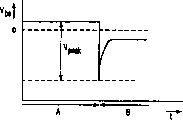
图2示意性地表示当第一晶体管截止时,第一晶体管的基极和发射极之间的可能的电压响应特性;Fig. 2 schematically represents a possible voltage response characteristic between the base and the emitter of the first transistor when the first transistor is turned off;
图3示意性地表示与工厂测量和控制设备相连的按照本发明的控制电路;Fig. 3 schematically represents the control circuit according to the invention connected with the plant measurement and control equipment;
图4示意性地说明工厂测量和控制设备怎样调整按照本发明的控制电路,以便为负载的预定状态选择最佳调整状态。Figure 4 schematically illustrates how plant measurement and control equipment adjusts the control circuit according to the invention in order to select the optimum adjustment state for a predetermined state of the load.
图1中示出用来控制负载6、如阴极射线管(CRT)的偏转电路上的电信号4的按照本发明的控制电路2的一部分。在这种情况下,电信号是流过晶体管8的集电极10和发射极12的电流I4。控制电路包括用来控制负载6上电流I4的通断的第一晶体管8。负载6与第一晶体管8的集电极10和发射极12相连。控制电路2还包括与第一晶体管8的基极16和发射极12相连、用来驱动第一晶体管8的谐振电路14。电源18经由脉冲发生电路20(从而间接连接)与谐振电路14相连,用来驱动谐振电路14。在图1的实例中,脉冲发生电路20还与含有存储单元26的处理单元24相连。脉冲发生电路20可通过图1中示意表示的脉冲信号22来开关第一晶体管8。在这个实例中,脉冲信号22由多个连续的方波脉冲组成。脉冲信号22包括与各个相继的交替时间间隔A和B相对应的交替的各个高电平和低电平。从时间间隔A的高电平向时间间隔B的低电平过渡处,有一个在图1中用箭头标出的陡峭下降沿。在这些沿的位置,晶体管12截止,使得电流4下降到大约零安培的值。脉冲发生电路20控制第一晶体管8通断的确切操作是一个由脉冲发生电路20、谐振电路14和电源18的复杂合作过程。由于这个合作过程本身是公知的,因而本专利申请将不对其进行详细描述。谐振电路14可以是一个LCR电路,参见例如图3。Figure 1 shows part of a
脉冲发生电路20产生脉冲信号22,其中在时间间隔A期间,第一晶体管8处于导通状态,所以最大电流I4流过第一晶体管8的集电极10和基极12。因此,存在三种可能的不同情况。The
在第一种情况中,第一晶体管8处于“转向不足”。这意味着流向第一晶体管8的基极16的基极电流太小而不能在集电极10和发射极12间产生可忽略的电压。这种情况下,甚至小的电流I4就能产生相当大的散热量,使第一晶体管的温度迅速增加。因此,在“转向不足”的情况下,在第一晶体管8中有较大的散热量。In the first case, the
第一晶体管8的第二种可能情况是“转向过度”,这意味着流向第一晶体管8的基极16的基极电流比由第一晶体管能产生最大电流I4的增益系数对应的基极电流值大。在时间间隔A向时间间隔B过渡时,流向基极16的基极电流将降到零。接下来,在第二种可能情况中,基极16上的电压可变成零或甚至是负值,其中基极电流可能改变符号,使得基极电流从基极16流出。结果,进入第一晶体管8的基极16的载流子数目迅速减少,并将变为零。减少基极16中的载流子数目将导致电流I4减小,同时由于感性负载6的性能,第一晶体管8的集电极和发射极之间的电压上升。在通过集电极10和发射极12的相应电流I4上升和下降期间,产生一个功率峰值,它将被耗散在第一晶体管8中。结果在第一晶体管8中出现较大的散热量。The second possible situation for the
在第三种情况中,驱动晶体管8,使其处于“转向不足”和“转向过度”两种状态之间。在第三种情况中,以最佳方式驱动晶体管8。这就称为第一晶体管8的最佳驱动,其中第一晶体管8中散热最小。第一晶体管8的这种最佳控制是这样一种情形,其中第一晶体管8的基极16的电压具有在基极16上的最大(负的)峰值电压Vp。In the third case,
装有包含控制电路2的最佳控制调整的控制信息的处理单元24的任务是用来以这样的方式控制所述控制电路2,即第一晶体管8由具有最佳控制调整的最佳驱动来控制。The task of the
当脉冲发生电路20通过脉冲信号22使晶体管8截止时,流入第一晶体管的基极16的基极电流将是负电流(这样电流从晶体管8的基极16流出),它在短时间内上升到大约零值。这样从基极16流出的基极电流流入谐振电路14。谐振电路14可包括LCR电路。这产生在图2中示意表示成t(时间)的函数的电压响应特性VBE。这个电压响应特性的幅度取决于第一晶体管8的基极16中的基极电流上升速度和电流I4的大小。如果第一晶体管8没有“转向不足”和“转向过度”,则达到的电压峰值Vp将是最大的。结果,达到的峰值表明第一晶体管8的最佳控制。When the
控制电路2包括带有存储单元26的处理单元24,其中存储单元26装有控制信息。控制信息涉及负载6的预定状态和控制电路2的相应预定最佳控制调整。处理单元24被用来针对负载6的实际状态根据控制信息最佳地控制电源18。为此,处理单元24可以直接经由连接28与电源相连,但是处理单元也可以只经由连接30与脉冲发生电路20相连。在后一种情况下,处理单元24可通过脉冲信号22的脉宽调制以间接方式控制电源18。在任一方式中,脉冲发生电路20产生脉冲信号20,该信号的沿确定第一晶体管8的开关时间点。为了这个操作,脉冲发生电路20经由谐振电路14与第一晶体管8相连。The
重要的是注意,控制电路2可根据负载6的实际状态控制负载上的电信号4。如果负载6是CRT的偏转线圈,那么预定状态由一组状态参数来定义。可以定义这样一组状态参数,例如在30-120KHz区间中的行开关频率,不同图像尺寸等。负载的每个预定状态要求不同的电信号4和第一晶体管8的基极16的相应不同的基极电流。最佳值是使第一晶体管8耗散的电能尽可能少的那些值。其中第一晶体管8的热耗散最小的最佳控制调整是在峰值电压Vp最大的点实现的。It is important to note that the
稍后将借助于图3进行说明,这些最佳控制调整可能已在工厂里通过工厂测量和控制设备建立。建立最佳控制调整后,将其存储在处理单元24的存储单元26中。As will be explained later with the aid of Figure 3, these optimal control adjustments may already be established at the factory by factory measurement and control equipment. Once the optimal control adjustment has been established, it is stored in the
图3详细给出按照本发明的控制电路2的一个实施例,它与包括偏转电路的负载6以及工厂测量和控制设备34相连。FIG. 3 details an embodiment of a
控制电路2包括用于控制负载6上电信号I4通断的第一晶体管8。负载6与第一晶体管8的集电极10和发射极12相连。控制电路2还包括含有LCR电路的谐振电路14。LCR电路包括感抗36,诸如线圈、电阻38以及第一晶体管8的阻塞基极-发射极结的电容。The
谐振电路14与脉冲发生电路20相连,脉冲发生电路20包括第二晶体管42、与第二晶体管42的基极和发射极相连的脉冲发生器44以及变压器46。变压器46的第一线圈48与电源18和第二晶体管42的集电极相连。此外,变压器46的第二线圈50与谐振电路14相连。最后,脉冲发生电路20包括与地以及同时连接到第一线圈46和电源18的结点相连的耦合电容器52。The
在这个实例中,电源18包括与地和压控电流源56相连、用于产生电源电压54的基本驱动器54。压控电流源56与所述结点和数模转换器58相连。数模转换器58是处理单元24和电源电压18的接口。在这个实例中,处理单元24是含有存储单元26的微处理器。In this example, the
负载6包括如图3示意表示的偏转电路。负载6包括与第一晶体管8的集电极10和负载6的其它元件相连的集电极串联二极管60。这些其它元件是回扫二极管62、回扫电容器64、与偏转电源电压68串联连接的电源耦合线圈66以及与偏转线圈72的并联连接和隔直电容74串联连接的线性校正器70。图3中的负载6的偏转电路本身是已知的,这里不作详细描述。这里要注意的重要事情是,偏转电路可处于随状态参数而定的不同状态,这些参数包括诸如用于行偏转的不同开关频率以及CRT的屏幕上显示的不同图像格式。The
在图3的示例中,控制电路2经由连接76和78与工厂测量和控制设备34相连。工厂测量和控制设备34包括峰值整流二极管80,它与用于设置峰值电压整流器的时间常数的放电电阻82和用于对经连接76在第一晶体管8的基极16测得的峰值电压Vpeak整流的储能电容器84的并联连接相串联。峰值整流二极管80、放电电阻82和储能电容器84与模数转换器86相连。模数转换器86与测量和控制设备34的测量和控制处理单元88相连。测量和控制处理单元88经由连接78与控制电路2的处理单元24相连。In the example of FIG. 3 , the
在下文中,详细说明通过工厂测量和控制设备34调整控制电路2的方法。Hereinafter, a method of adjusting the
在工厂里,控制电路2可通过连接76、78与工厂测量和控制设备34相连。那么就开始测量和调整循环,其中工厂测量和控制设备34还通过控制连接90与负载6相连。然后,负载6被调整到其预定状态之一。在这个预定状态,测量和控制处理单元88通过连接78控制处理单元24,使得处理单元24在第一控制调整中控制电源18。同时,脉冲发生电路20驱动用于驱动第一开关晶体管8的谐振电路14,这里脉冲信号的沿确定开关时间点。然后,工厂测量和控制设备34经过连接76测量基极16和发射极12之间的实际电压。图2给出基极16和发射极12之间的所测电压VBE的一个例子。函数VBE是电压响应特性。如图2所示,在时间间隔A,第一晶体管的基极和发射极之间的电压基本上是恒定值。然后,在从时间间隔A向时间间隔B过渡时,电压VBE下降一个峰值电压Vpeak,这里电压VBE可能变为负的,随后上升为零或负值。这个值Vpeak是用于确定控制电路2的最佳控制调整的重要参数,特别是用于最佳驱动或调整第一晶体管8的重要参数。在负载6的预定状态下,工厂测量和控制设备34将为电源18的不同控制调整测量峰值电压Vp。然后,通过选择其中Vp最大的特定电压响应特性VBE来确定用于预定状态的最佳控制调整。图4示意性地说明了这一过程。沿着图4坐标系的纵轴测量Vpeak值,沿水平轴测量压控电流源56产生的电流Ip92。在由工厂测量和控制设备34完成的第一调整中,压控电流源56把电流Ip驱动到脉冲发生电路20。然后,作为响应,测量峰值电压Vpeak=Vpl并由工厂测量和控制设备34存储。然后,在第二调整中,电流Ip92由相应的峰值电压Vp2产生。这一过程一直持续到为最佳控制调整I3找到最大可能的峰值电压Vp3。这个最佳控制调整由工厂测量和控制设备34经由连接78存入处理单元24的存储单元26。存储单元26最好是用来存储信息的EEPROM单元。In the factory, the
接下来,对于负载6的其它预定状态,工厂测量和控制设备34执行前述段落所描述的过程。这样,对负载的每个预定状态,找到最佳控制调整,可存储在处理单元24的存储单元26中。Next, for other predetermined states of the
在工厂测量和控制设备34针对负载6的预定状态建立最佳控制调整后,断开连接76、78、90,然后控制单元和负载6可以交付使用。控制电路2和负载6的组合能够以最佳方式工作,其中对于负载6的每个预定状态,控制电路都能够以最佳方式驱动第一晶体管8。这由不包括反馈环路的控制序列来完成。这种情况下,控制序列包括处理单元24、数模转换器58、电源18、脉冲发生电路20以及与第一晶体管8相连的谐振电路14。因为控制序列中没有反馈环路,所以可以实现第一晶体管8的稳定可靠的最佳控制。结果,第一晶体管8表现出最小的热耗散,使得控制电路2加负载6的结合能够表现最佳。After the factory measurement and
本发明是按照几个实施例来描述的。然而,本发明决不仅限于这些实施例。所述实施例的修改和变形也被认为落入本发明的范围内。此外,按照本发明的控制电路的宽应用范围也是可能的。例如,相应的控制电路可以被用在开关式电源、灯驱动电路和电动机控制电路中。The invention has been described in terms of several embodiments. However, the present invention is by no means limited to these Examples. Modifications and variations of the described embodiments are also considered to fall within the scope of the invention. Furthermore, a wide range of applications of the control circuit according to the invention is possible. For example, corresponding control circuits can be used in switching power supplies, lamp driving circuits and motor control circuits.
Claims (8)
Applications Claiming Priority (2)
| Application Number | Priority Date | Filing Date | Title |
|---|---|---|---|
| EP02077408.9 | 2002-06-18 | ||
| EP02077408 | 2002-06-18 |
Publications (1)
| Publication Number | Publication Date |
|---|---|
| CN1663234A true CN1663234A (en) | 2005-08-31 |
Family
ID=29724509
Family Applications (1)
| Application Number | Title | Priority Date | Filing Date |
|---|---|---|---|
| CN038138948A Pending CN1663234A (en) | 2002-06-18 | 2003-05-27 | Control circuit and method for controlling an electrical signal over a load such as a deflection circuit of a cathode ray tube |
Country Status (6)
| Country | Link |
|---|---|
| US (1) | US20050225267A1 (en) |
| EP (1) | EP1518396A1 (en) |
| JP (1) | JP2005530412A (en) |
| CN (1) | CN1663234A (en) |
| AU (1) | AU2003233098A1 (en) |
| WO (1) | WO2003107654A1 (en) |
Family Cites Families (7)
| Publication number | Priority date | Publication date | Assignee | Title |
|---|---|---|---|---|
| JP2535395B2 (en) * | 1988-12-23 | 1996-09-18 | 株式会社日立製作所 | Image display device |
| JPH0769670B2 (en) * | 1990-08-03 | 1995-07-31 | インターナシヨナル・ビジネス・マシーンズ・コーポレーション | Power supply |
| US5397914A (en) * | 1992-04-30 | 1995-03-14 | Hitachi Ltd. | Power transistor device including power transistors in darlington connection and zener diode which is coupled between collector and base of power transistors and which is formed in polysilicon film |
| JP3413333B2 (en) * | 1996-11-13 | 2003-06-03 | アルプス電気株式会社 | Signal detection circuit |
| KR200179722Y1 (en) * | 1997-11-25 | 2000-05-01 | 윤종용 | Display device having horizontal screen size adjustment circuit of step-up method |
| WO2000046924A1 (en) * | 1999-02-05 | 2000-08-10 | Koninklijke Philips Electronics N.V. | Driving a switching transistor |
| JP2001333392A (en) * | 2000-05-23 | 2001-11-30 | Matsushita Electric Ind Co Ltd | Horizontal deflection circuit and television receiver |
-
2003
- 2003-05-27 CN CN038138948A patent/CN1663234A/en active Pending
- 2003-05-27 EP EP03727849A patent/EP1518396A1/en not_active Withdrawn
- 2003-05-27 WO PCT/IB2003/002332 patent/WO2003107654A1/en not_active Ceased
- 2003-05-27 AU AU2003233098A patent/AU2003233098A1/en not_active Abandoned
- 2003-05-27 JP JP2004514330A patent/JP2005530412A/en not_active Withdrawn
- 2003-05-27 US US10/518,178 patent/US20050225267A1/en not_active Abandoned
Also Published As
| Publication number | Publication date |
|---|---|
| WO2003107654A1 (en) | 2003-12-24 |
| EP1518396A1 (en) | 2005-03-30 |
| US20050225267A1 (en) | 2005-10-13 |
| JP2005530412A (en) | 2005-10-06 |
| AU2003233098A1 (en) | 2003-12-31 |
Similar Documents
| Publication | Publication Date | Title |
|---|---|---|
| KR100233192B1 (en) | Piezoelectric transformer drive circuit | |
| US7920390B2 (en) | DC-AC converter, controller IC therefor, and electronic apparatus utilizing such DC-AC converter | |
| US6717375B2 (en) | Discharge lamp lighting device and system comprising it | |
| US7656102B2 (en) | Discharge lamp lighting circuit | |
| CN1778149A (en) | Discharge lamp lighting control device | |
| JPH10127058A (en) | Drive circuit for piezoelectric transformer | |
| CN111629496A (en) | Charge pump control circuit and driving power supply | |
| CN1052829C (en) | Power supply | |
| CN1179238A (en) | Power supply circuit | |
| EP2222141A1 (en) | Discharge lamp lighting circuit for AC-driving a discharge lamp | |
| CN1663234A (en) | Control circuit and method for controlling an electrical signal over a load such as a deflection circuit of a cathode ray tube | |
| CN1075311C (en) | Display device | |
| WO2000046924A1 (en) | Driving a switching transistor | |
| JPH07142178A (en) | Lamp drive circuit | |
| EP0989742A1 (en) | Horizontal deflection circuit | |
| US7443110B2 (en) | Discharge lamp energizing circuit and method of energizing discharge lamp | |
| JP4059053B2 (en) | Lighting method of high pressure discharge lamp | |
| CN1278541C (en) | Deflection circuit having feedback controlled capacitive transfer | |
| JP2993361B2 (en) | Horizontal deflection high voltage generation circuit | |
| CN219916689U (en) | Display apparatus | |
| EP2214459B1 (en) | Discharge lamp lighting circuit of double converter type | |
| EP0998133A1 (en) | Horizontal deflection circuit | |
| KR101995708B1 (en) | Plasma pulse power supply providing initially boosted pulse voltage | |
| JPH11127364A (en) | Horizontal deflection circuit | |
| CN117748911A (en) | DC conversion circuit and charger |
Legal Events
| Date | Code | Title | Description |
|---|---|---|---|
| C06 | Publication | ||
| PB01 | Publication | ||
| C10 | Entry into substantive examination | ||
| SE01 | Entry into force of request for substantive examination | ||
| C02 | Deemed withdrawal of patent application after publication (patent law 2001) | ||
| WD01 | Invention patent application deemed withdrawn after publication |