CN1663124A - Capacitive touch sensor architecture with unique sensor bar addressing - Google Patents
Capacitive touch sensor architecture with unique sensor bar addressing Download PDFInfo
- Publication number
- CN1663124A CN1663124A CN038143526A CN03814352A CN1663124A CN 1663124 A CN1663124 A CN 1663124A CN 038143526 A CN038143526 A CN 038143526A CN 03814352 A CN03814352 A CN 03814352A CN 1663124 A CN1663124 A CN 1663124A
- Authority
- CN
- China
- Prior art keywords
- sensor
- leads
- touch
- strips
- capacitive touch
- Prior art date
- Legal status (The legal status is an assumption and is not a legal conclusion. Google has not performed a legal analysis and makes no representation as to the accuracy of the status listed.)
- Pending
Links
Images


Classifications
-
- H—ELECTRICITY
- H03—ELECTRONIC CIRCUITRY
- H03K—PULSE TECHNIQUE
- H03K17/00—Electronic switching or gating, i.e. not by contact-making and –breaking
- H03K17/94—Electronic switching or gating, i.e. not by contact-making and –breaking characterised by the way in which the control signals are generated
- H03K17/96—Touch switches
- H03K17/962—Capacitive touch switches
- H03K17/9622—Capacitive touch switches using a plurality of detectors, e.g. keyboard
-
- H—ELECTRICITY
- H03—ELECTRONIC CIRCUITRY
- H03K—PULSE TECHNIQUE
- H03K17/00—Electronic switching or gating, i.e. not by contact-making and –breaking
- H03K17/94—Electronic switching or gating, i.e. not by contact-making and –breaking characterised by the way in which the control signals are generated
- H03K17/96—Touch switches
-
- G—PHYSICS
- G06—COMPUTING OR CALCULATING; COUNTING
- G06F—ELECTRIC DIGITAL DATA PROCESSING
- G06F3/00—Input arrangements for transferring data to be processed into a form capable of being handled by the computer; Output arrangements for transferring data from processing unit to output unit, e.g. interface arrangements
- G06F3/01—Input arrangements or combined input and output arrangements for interaction between user and computer
- G06F3/03—Arrangements for converting the position or the displacement of a member into a coded form
- G06F3/041—Digitisers, e.g. for touch screens or touch pads, characterised by the transducing means
- G06F3/044—Digitisers, e.g. for touch screens or touch pads, characterised by the transducing means by capacitive means
- G06F3/0443—Digitisers, e.g. for touch screens or touch pads, characterised by the transducing means by capacitive means using a single layer of sensing electrodes
Landscapes
- Engineering & Computer Science (AREA)
- General Engineering & Computer Science (AREA)
- Theoretical Computer Science (AREA)
- Human Computer Interaction (AREA)
- Physics & Mathematics (AREA)
- General Physics & Mathematics (AREA)
- Position Input By Displaying (AREA)
- Measurement Of Length, Angles, Or The Like Using Electric Or Magnetic Means (AREA)
- Electronic Switches (AREA)
Abstract
Description
发明领域Field of Invention
本发明涉及电容性接触式传感器架构。更具体地说,本发明涉及能够提供指示屏幕或传感器的何处被触及的相当精确的控制信号的电容性接触式传感器。The present invention relates to capacitive touch sensor architectures. More specifically, the present invention relates to capacitive touch sensors capable of providing fairly precise control signals indicative of where a screen or sensor is touched.
发明背景Background of the Invention
触摸屏与包括阴极射线管(如CRT)和液晶显示屏(如LCD屏幕)的各类显示器一起使用,作为向计算机系统输入信息的装置。当置于显示屏之上时,触摸屏允许用户通过触摸对应于所希望的图标或元素的屏幕位置,来选择显示的图标或元素。随着计算机和其它电子设备变得越来越普及,触摸屏正越来越成为普遍的数据输入接口。例如,如今,在车间、仓库、生产设备、饭店、手持个人数字助理、自动出纳机、游乐场游戏机等中,都可以发现触摸屏的存在。Touch screens are used with various types of displays, including cathode ray tubes (eg, CRTs) and liquid crystal displays (eg, LCD screens), as a means of inputting information to computer systems. When placed over a display screen, a touch screen allows a user to select a displayed icon or element by touching the screen location corresponding to the desired icon or element. As computers and other electronic devices become more popular, touch screens are becoming an increasingly common data entry interface. For example, today, touch screens can be found in workshops, warehouses, production facilities, restaurants, handheld personal digital assistants, automated teller machines, arcade game machines, and more.
一种类型的触摸屏,即电容性触摸屏,包括电容性传感器电路,该电容性传感器电路具有多个传感器条(sensor bar),每个传感器条产生电场。通常,但非必然,用诸如窗玻璃之类的光学透明的防护材料来叠层于传感器电路。邻近于一个或多个传感器条的触摸对电场进行调制,并产生信号。使用将传感器电路电气连接到控制器的引线(lead line)网络,将该信号从传感器条传送到控制器。控制器对信号进行解析,以确定触摸屏幕的位置。然后可把位置的X-Y坐标传送给另一处理器,进行进一步的处理,例如传送给一计算机用于输入对屏幕上显示和选择项目的命令(order)。One type of touch screen, the capacitive touch screen, includes a capacitive sensor circuit with a plurality of sensor bars, each sensor bar generating an electric field. Typically, but not necessarily, an optically transparent protective material such as window glass is laminated to the sensor circuitry. A touch adjacent to one or more sensor bars modulates the electric field and generates a signal. This signal is carried from the sensor strip to the controller using a network of lead lines that electrically connect the sensor circuit to the controller. The controller interprets the signal to determine where the screen was touched. The X-Y coordinates of the position can then be sent to another processor for further processing, such as to a computer for inputting orders for on-screen display and selection of items.
传统的电容性接触式传感器架构影响了精确解析触摸位置的能力。传统上,将传感器条连接到控制器的每条引线连接到多个传感器条。为此,某一引线上的信号可能指示出不止一个单个传感器条上的触摸。传统的接触式传感器设计采用的布局是,使一端的引线上出现的信号与另一端的引线上出现的信号进行比较。所述比较使控制器解析出多个传感器条中的哪个传感器条实际上经历了触摸。换言之,传统的接触式传感器将不同的一组引线耦合到传感器条的每一端,从而接触式传感器的一端上存在的信号与另一端上存在的信号一起唯一地定义了每个传感器条。Traditional capacitive touch sensor architectures compromise the ability to accurately resolve touch location. Traditionally, each lead that connects a sensor strip to a controller is connected to multiple sensor strips. For this reason, a signal on a certain lead may indicate a touch on more than one individual sensor bar. Traditional touch sensor designs use a layout where the signal appearing on the leads at one end is compared to the signal appearing on the leads at the other end. The comparison allows the controller to resolve which of the plurality of sensor bars actually experienced a touch. In other words, conventional touch sensors couple a different set of leads to each end of a sensor strip such that the signal present on one end of the touch sensor together with the signal present on the other end uniquely defines each sensor strip.
触摸屏的设计者面临的问题是设计制造经济且能精确地建立触摸位置的触摸屏和传感器电路。The problem facing the designer of a touch screen is to design a touch screen and sensor circuitry that is economical to manufacture and that accurately establishes the location of a touch.
发明概述Summary of Invention
本发明针对一种提供改进的电容性触摸屏的装置和方法。本发明包括配置用于部署在屏幕上的多个平行的传感器条。在一个方面,本发明提供对称架构,其中每个传感条(sensing bar)连接到唯一的一对引线,传感条的一端连接到一对引线中的一条引线,而该传感条的另一端连接到该对引线中的另一条引线。The present invention is directed to an apparatus and method for providing an improved capacitive touch screen. The present invention includes a plurality of parallel sensor strips configured for deployment on a screen. In one aspect, the present invention provides a symmetrical architecture in which each sensing bar is connected to a unique pair of leads, one end of the sensing bar is connected to one of the pair of leads, and the other end of the sensing bar is connected to a unique pair of leads. One end is connected to the other lead of the pair.
在另一方面,本发明可配置成减少引线在接触式传感器各端上所占据的空间。本发明将引线配置成沿传感器的相对的两边配置的引线的总和近似等于传感器条的数量。In another aspect, the present invention can be configured to reduce the space occupied by the leads on each end of the touch sensor. The present invention configures the leads such that the sum of the leads disposed along opposite sides of the sensor is approximately equal to the number of sensor strips.
在又一方面,第一组引线中的引线数基本等于第二组引线中的引线数。接触式传感器的传感器条定向于与尾部电路平行。通过将引线从传感器条的一端沿接触式传感器的两侧布线,减少了接触式传感器两侧上所需的空间量,使得可将主设备制造得更小而不减小接触式传感器的大小,或者可将接触式传感器制造得稍微大一点,而不影响主设备的大小。In yet another aspect, the number of leads in the first set of leads is substantially equal to the number of leads in the second set of leads. The sensor bar of the touch sensor is oriented parallel to the tail circuit. By routing the leads from one end of the sensor strip along both sides of the touch sensor, the amount of space required on both sides of the touch sensor is reduced, allowing the host device to be made smaller without reducing the size of the touch sensor, Or the touch sensor can be made slightly larger without compromising the size of the host device.
附图简述Brief description of the attached drawings
当结合示意性的但非等比例的附图时,通过参考下面的详细描述,将更容易地理解本发明的上述方面和所伴随的许多优点,附图中:The foregoing aspects of the invention, and the many attendant advantages thereof, will be more readily understood by reference to the following detailed description when taken in conjunction with the schematic, not to scale accompanying drawings, in which:
图1是说明示例性系统概述的示意图;Figure 1 is a schematic diagram illustrating an exemplary system overview;
图2是根据本发明的示例性电容性接触式传感器的示意图;2 is a schematic diagram of an exemplary capacitive touch sensor according to the present invention;
图3是根据本发明的接触式传感器的一部分的实施例的示意图;Figure 3 is a schematic diagram of an embodiment of a portion of a touch sensor according to the present invention;
图4a和4b是根据本发明的替代实施例的接触式传感器的一部分的示意图;4a and 4b are schematic diagrams of a portion of a touch sensor according to an alternative embodiment of the present invention;
图5是对接触式传感器中的传感器条的触摸的示意图;5 is a schematic diagram of a touch to a sensor bar in a touch sensor;
图6a-6c是示出对于四个相邻传感器条的信号幅度绘图的示意图。6a-6c are schematic diagrams showing signal magnitude plots for four adjacent sensor strips.
较佳实施例的详细描述Detailed description of the preferred embodiment
在本发明的示例性实施例的下述详细描述中,参考构成本发明的一部分的附图。详细描述以及附图说明了可实施本发明的具体示例性实施例。对这些实施例的详细描述足以使本领域的技术人员实施本发明。要理解,可采用其它实施例,并可作出其它改变,而不背离本发明的要旨和范围。因此,不应把下述详细描述理解为限制性的,本发明的范围仅由所附的权利要求来定义。In the following detailed description of exemplary embodiments of the invention, reference is made to the accompanying drawings which form a part hereof. The detailed description and drawings illustrate specific exemplary embodiments in which the invention may be practiced. The detailed description of these examples is sufficient to enable those skilled in the art to practice the invention. It is to be understood that other embodiments may be utilized, and other changes may be made, without departing from the spirit and scope of the present invention. Accordingly, the following detailed description should not be taken as limiting, and the scope of the present invention is defined only by the appended claims.
贯穿说明书以及权利要求书,除非另外清楚地指示出,否则下述的术语采用与之明确相关联的含义。“一(个)”、“所述”的含义包括复数引用。“在...中”的含义包括“在...中”和“在...上”。关于附图,在整个附图中,相同的标号表示相同的部分。此外,除非另外指明或除非与这里的揭示不符,否则对单数的引用包括对复数的引用。Throughout the specification and claims, the following terms take the meanings explicitly associated therewith unless clearly indicated otherwise. The meanings of "one (one)" and "the" include plural references. The meaning of "in" includes "in" and "on". With regard to the drawings, like reference numerals designate like parts throughout the drawings. Furthermore, references to the singular include references to the plural unless otherwise indicated or unless otherwise inconsistent with the disclosure herein.
简而言之,本发明涉及一种电容性接触式传感器架构,具有对多个传感器条的每一个的分立的引线连接。本发明能够精确地解析触摸位置。通过接收的来自被触摸的传感条的左信号和右信号的比率来确定沿传感条的坐标。传感器条及其引线的左部和右部之间的电气特性的不平衡可能造成比率的不精确,会不利地影响触摸位置的确定。本发明的接触式传感器架构通过将每个传感器条连接到唯一的一对引线,提供了传感器条及其引线的对称的或平衡的电气特性。来自被触摸的传感器条的电信号及其唯一的引线可用于控制器根据任何适当的方法来确定触摸位置。Briefly, the present invention relates to a capacitive touch sensor architecture with separate wire connections to each of a plurality of sensor strips. The present invention can accurately analyze the touch position. The coordinates along the sensor strip are determined by the ratio of the received left and right signals from the touched sensor strip. Imbalances in the electrical characteristics between the left and right portions of the sensor bar and its leads can cause inaccuracies in the ratio that can adversely affect touch location determination. The touch sensor architecture of the present invention provides symmetrical or balanced electrical characteristics of the sensor strips and their leads by connecting each sensor strip to a unique pair of leads. The electrical signal from the touched sensor strip and its sole lead may be used by the controller to determine the location of the touch according to any suitable method.
图1是说明电容性接触式传感器的一般操作原理的示意图。图1中,触摸屏系统100包括接触式传感器101、控制器122、以及计算机126。在该特定实施例中,接触式传感器101除了标准的玻璃层之外,还包括电容性接触式传感层,如按照本发明所构造的一个电容性接触式传感层。FIG. 1 is a schematic diagram illustrating the general principle of operation of a capacitive touch sensor. In FIG. 1 , a
在操作中,控制器122向接触式传感器101的电容性接触式传感层提供激励波形,在电容性传感层中产生电场。当触摸或非常接近接触式传感器101时,由于手指尖与接触式传感层之间的电容性耦合,电场中发生可检测到的变化或调制。电场中的这种变化或调制产生了与物体与接触式传感器101的接近程度和位置成比例的信号。控制器122感测出反映电场中的变化的信号。控制器122通过若干方法中的一种方法对触摸进行解析,获得表示触摸位置的一组笛卡尔坐标。位置图140是接触式传感器101上的实际触摸位置的图形表示。触摸位置的坐标提供给另一设备,例如提供给计算机126,以执行屏幕上显示和触摸的命令。贯穿于本说明书、权利要求书以及附图,在物体接近于接触式传感器101使得电容性耦合发生,从而引起电场的调制的情况下,认为发生了“触摸”。并不需要发生实际的接触。物体可以是任何电导性的物体,如身体部分(一般是手指)或非生物物体(一般是触笔)。In operation,
图2是说明根据本发明的一个实施例的电容性接触式传感器的等角图。在该实施例中,触摸屏200包括接触式传感器电路218、传感器电路部电路(tail)220、第一元件212、第二元件216、以及粘合剂214。Figure 2 is an isometric view illustrating a capacitive touch sensor in accordance with one embodiment of the present invention. In this embodiment,
触摸屏220可包括若干层。第一元件212和第二元件216代表用于接触式传感器电路218的保护基板。这两个元件一般可以是任何非导电的材料,并可通过化学加固的玻璃板、钢化的玻璃板或具有类似性质的其它透明材料来制造。在光学透明性并非必须的应用中,如触板应用中,第一元件212和第二元件216无需是光学透明的或是玻璃的。可使用任何适当的材料,如塑料或其它非导电材料。此外,在某些实施中,希望用诸如聚酯材料之类的柔性材料制造第一元件212和第二元件216,以实现可形变的或可弯曲的接触式传感器。The
粘合剂214置于第一元件212和第二元件216之间。接触式传感器电路218配置在第二元件216之上,并通过传感器电路尾部电路220与其它电路进行电气通信。诸元件形成了适用于与LCD屏幕、CRT屏幕、触板、和不论是否可视的任何其它设备一起使用的夹层结构210。在一替代实施例中,接触式传感器电路218可固定或直接应用于LCD屏幕、CRT屏幕或其它类似的可视设备的观看表面,而无需第二元件216。
在操作中,接触式传感器电路218接收来自控制器的电信号,并再产生电场,接收对第一元件212的触摸,并产生一个在传感器电路尾部电路220输出的、表示由于触摸和接触式传感器电路218之间的电容性耦合造成的电场的调制的信号。In operation, the
本发明所带来的优点增加了触摸屏设计者的灵活性。例如,传感器电路的提高的精确性允许在接触式传感器电路218上使用更厚的保护元件(如第一元件212),同时仍然保持相同的解析精确性。为此,本发明的各种实施方式可利用比不可替换的保护元件大一些的可替换的或可去除的保护元件。这样一种实施方式在户外公用电话亭等场所中具有特别的适用性,在这些场所中,天气或故意的破坏行为常常引起对触摸屏的外层保护元件的损坏。本发明以更低的成本、更可行地提供覆盖接触式传感器的可替换的保护元件,而不会使性能有任何显著劣化。The advantages brought by the present invention increase the flexibility of touch screen designers. For example, the increased accuracy of the sensor circuit allows the use of thicker protective elements (eg, first element 212 ) on
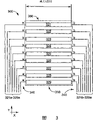
图3是示出用于触敏式屏幕的示例性接触式传感器电路300的本发明的一个实施方式的示意图。图3中,接触式传感器电路300包括多个传感器条310、包括独立的“a”端引线321a-329a的一组“a”端引线340、包括独立的“b”端引线321b-329b的一组“b”端引线345、以及观看表面周边360。FIG. 3 is a schematic diagram of one embodiment of the invention illustrating an exemplary
更为具体地来说,接触式传感器电路300包括从观看表面周边360的一侧跨越到另一侧的若干触敏式传感器条310(“条”)。在一替代实施例中,多个传感器条310中的各传感器条实质上是平行的,或者换句话说是以长度方向定向或配置于单一的方向中。传感器条310较佳地具有在传感器条的长度上基本线性的电气特性。它们较佳地用铟锡氧化物(ITO)构造,用于光学透明的应用场合,但也可用任何适当的导电材料构造。在任一应用中采用的传感器条的数量可按照该特定应用的设计参数而改变。图3说明了具有9个传感器条321-329的实施例。More specifically,
在一替代实施例中,除了矩形之外,传感器条310的各传感器条可以是各种配置和形状,导电材料均匀淀积在周边内。例如,各传感器条可包括导电周边和位于导电周边内的非导电区域。传感器条可以是能够响应于触摸而建立表示触摸位置的输入信号的任何形状。In an alternate embodiment, each sensor strip of
根据本发明,每个传感器条310连接到自己唯一的一对导电引线。引线可以是导线、迹线、或适用于将传感器条连接到控制器(122,图1)的其它电路或系统。例如,传感器条324在其第一端连接到引线324a,而在其第二端连接到引线324b。引线324a和324b然后连接到控制器,如图1的控制器122。在一个实施例中,“a”端引线321a-329a和“b”端引线321b-321b可集中于传感器电路尾部电路220中,该尾部电路具有连接到控制器的导电连接器。虽然示出集中在图2中的传感器电路尾部电路220中,但是任何手段都足以将线路连接到控制器(未示出)。一般来说,线路可由实际上任何导电材料制成,如铜、银、金等。如果线路印刷在膜上,则希望膜与导电材料不发生反应。In accordance with the present invention, each
为便于说明,连接到任一特定传感器条的各端的引线具有相同的标记。“a”端引线340位于接触式传感器电路300的一端,“b”端引线345位于图3的另一端。各传感器条321-329通过其自己唯一的一对引线连接到控制器。例如,传感器条324的两端通过引线324a和324b连接到控制器。没有其它传感器条连接到引线324a或324b。本发明的这一特征允许对各传感器条唯一地寻址,可立即将一对引线上出现的信号解析到经历触摸的特定传感器条。图3说明了传感器条310和它们的唯一的引线是对称布局的,且各对引线的“a”端引线和“b”端引线连接到同一传感器条的相对的两端中的各自的一端。为了进行这种说明,将彼此相邻的传感器条定义为“邻居”。将传感器条310的间距和大小选择成使得在任一传感器条上的触摸在该传感器条的最接近的第一和第二邻居上产生合理的信号。For ease of illustration, the leads connected to each end of any particular sensor strip have the same label. Terminal "a"
在操作中,引线340和345接收来自控制器的激励波形,并将其提供给传感器条310,传感器条再产生电场。接触式传感器电路300接收对一个或多个传感器条310的触摸,作为响应,在一对或多对唯一引线340和345上产生信号。所述信号表示由于触摸和一个或多个传感器条310之间的电容性耦合造成的电场中的变化。In operation, leads 340 and 345 receive an excitation waveform from the controller and provide it to
由于每个传感器条及其引线不连接到任何其它传感器条或引线,因此对某一传感器条的区域中的触敏式屏幕的触摸,如靠近传感器条328的触摸346,将在连接到该传感器条的一对引线(如引线328a和328b)上产生信号,而与任何其它传感器条或引线无关。此外,触摸346可能耦合到相邻的传感器条(327和329)。在这种情况下,触摸将在与之连接的各线路(327a-b、329a-b)上产生唯一的信号,各信号完全与任何其它传感器条或引线无关。对采用接触式传感器电路300的屏幕的触摸应在受触摸的传感器条上产生的峰值信号,在受触摸的传感器条的相邻邻居上产生较小的或降低的信号。从而,对屏幕的任何触摸应导致连接到与该触摸相邻近的传感器条的若干线路上的唯一的独立信号的一种图案。Since each sensor bar and its leads are not connected to any other sensor bar or leads, a touch to the touch-sensitive screen in the area of a certain sensor bar, such as touch 346 near
如随后将明白的那样,由于对称架构为每个传感器条提供唯一的一对引线,本发明还提供了精确地解析发生在X轴上的触摸的位置的能力。本发明提供在X方向和Y方向的高精确性。本发明还提供通过分析信号来识别受触摸的传感器条以及在触摸发生的区域中的相邻传感器条,解析Y轴上发生的触摸的位置的能力。本发明的进一步的优点在于可在单个步骤中形成引线,因为不存在交叉或多个连接。图3提供了根据本发明的教义建立的传感器电路的一个例子。As will become apparent later, the present invention also provides the ability to precisely resolve the location of a touch occurring on the X-axis due to the symmetrical architecture providing each sensor bar with a unique pair of leads. The present invention provides high accuracy in the X and Y directions. The present invention also provides the ability to resolve the location of a touch on the Y-axis by analyzing the signal to identify the touched sensor bar and adjacent sensor bars in the area where the touch occurred. A further advantage of the present invention is that the leads can be formed in a single step since there are no crossovers or multiple connections. Figure 3 provides an example of a sensor circuit built according to the teachings of the present invention.
图4A和4B是根据本发明的替代实施例的接触式传感器的一部分的示意图。图4a是触摸屏系统400的一个实施方式的示意图。该实施方式是在具有表面405、按键407、侧边区域(side area)430和435、以及触摸屏的手持设备420中实施的。触摸屏由具有接触式传感器电路450的电容性接触式传感器条410(图4B详述)的接触式传感器401组成。接触式传感器401配置成与图1所说明的触摸屏系统100基本类似的方式操作。4A and 4B are schematic diagrams of a portion of a touch sensor according to an alternative embodiment of the present invention. FIG. 4 a is a schematic diagram of one embodiment of a
手持设备420可以具有个人数字助理(PDA)和其它设备的性质,其中由于设计局限,接触式传感器401和设备的周边之间的侧边区域430和435很小。应理解,为了便于说明,侧边区域430和435的大小在图中被夸大,并且,可以表现为侧边区域430和435相对于手持设备420的尺寸来说是较小的。在图4a所说明的实施例中,接触式传感器电路以垂直的接触式传感器条410定向,即近似平行于侧边区域430和435的传感器条。
图4B说明了关于图4A所说明的接触式传感器401的其它细节。接触式传感器450包括多个传感器条410、“a”端引线421a-426a、“b”端引线421b-426b、传感器条421-426、观看表面周边460(以虚线框示出)、第一组引线470以及第二组引线480。FIG. 4B illustrates additional details regarding the
更为具体地来说,接触式传感器电路450包括跨越由周边460例示出的接触式传感器401的多个传感器条421-426。传感器条410可以是实质上平行的。在一替代实施例中,传感器条410可以以长度方向定向,或配置于单一方向中,而不用实质上是平行的。接触式传感器电路450配置成与图3的接触式传感器电路300基本类似,不同在于引线421b-426b组合成第一组引线470和第二组引线480。第一组引线470和第二组引线480布线成使得(i)它们与传感器条410大体平行;(ii)它们位于屏幕周边460的相对的两端(第一端和第二端);以及(iii)第一组引线470和第二组引线480的引线总数近似等于传感器410的数量。More specifically,
在一个实施例中,第一组引线470的引线数与第二组引线480的引线数实质相同。通过将传感器条421-426以与手持设备420的方向相垂直地定向,并通过将引线从传感器条410的一端沿接触式传感器401的两端布线,就降低了侧边区域430和435所必需的空间量,从而可使手持设备420更小,而不用减小接触式传感器401的大小,或者可稍微增大接触式传感器401,而不影响手持设备420的大小。换言之,这种引线配置减少了侧边区域430和435,并使得接触式传感器401占据手持设备420的更多的宽度。In one embodiment, the number of leads in the first set of
图4B和4C所说明的配置在希望检测多于单个触摸的娱乐活动中具有特别的适用性。例如,可用图4B所说明的接触式传感器电路450的实施方式构造游戏设备。该游戏设备可在触摸屏的不同部分提供分开的用户输入区。例如,该游戏设备可利用分开的并肩的游戏区域支持二人游戏。在此情况中,由于触摸将在具有唯一引线的传感器条上产生信号,因此可容易地检测出两个分开的同时的触摸(在各游戏区域中的触摸),从而不会出现歧义。The configuration illustrated in Figures 4B and 4C has particular applicability in entertainment activities where it is desired to detect more than a single touch. For example, a gaming device may be constructed with the embodiment of
作为替代,图4C中说明的配置可用于与上述类似的应用场合。在该例子中,提供具有两个输入区(493、494)的接触式传感器490。在该实施方式中,各输入区(493、494)包括六个分立寻址的传感器条,各传感器条连接到唯一的一对引线。左端输入区495的传感器条以如上所述的方式连接到第一组引线对497。类似地,右端输入区494的传感器条连接到第二组引线对498。各输入区的引线可连接到同一控制器或分立的控制器。各输入区(493、494)甚至可以是分开组装的接触式传感器单元,并肩安装来形成外观上呈现为单个的接触式传感器492。在该配置中,两个独立的触摸(例如触摸495和触摸496)可同时发生,但仍然能够彼此相区分。这种配置使得图4C的接触式传感器490尤其适用于对接触式传感器490的多个触摸可能同时发生的应用场合,如多用户游戏环境。这些仅仅是本发明所能实现的许多具体实施方式中的一些。Alternatively, the configuration illustrated in Figure 4C may be used in applications similar to those described above. In this example, a touch sensor 490 with two input fields (493, 494) is provided. In this embodiment, each input field (493, 494) includes six discretely addressed sensor strips, each connected to a unique pair of leads. The sensor strips of the left end input area 495 are connected to the first set of lead pairs 497 in the manner described above. Similarly, the sensor strip of the right end input field 494 is connected to a second set of lead pairs 498 . The leads for each input zone can be connected to the same controller or to separate controllers. Each input zone ( 493 , 494 ) could even be a separately assembled touch sensor unit, mounted side by side to form what appears to be a single touch sensor 492 . In this configuration, two separate touches (such as touch 495 and touch 496) can occur simultaneously and still be distinguishable from each other. This configuration makes the touch sensor 490 of FIG. 4C particularly suitable for applications where multiple touches to the touch sensor 490 may occur simultaneously, such as a multi-user gaming environment. These are just a few of the many specific embodiments that are possible with the present invention.
图5说明了本发明的一个方面,其中连同本发明一起工作的控制器能够从触摸产生的信号中解析X轴坐标。接触式传感器500的配置和操作与图3所说明的接触式传感器300基本类似。图5是说明触摸T1发生在一传感器上或其附近,另外两个触摸T2和T3发生在传感器电路的周边附近的示意图。Figure 5 illustrates an aspect of the invention in which a controller working in conjunction with the invention is able to resolve an X-axis coordinate from a touch-generated signal. The configuration and operation of touch sensor 500 is substantially similar to
为了理解本发明提供的坐标解析方法,重要的是认识到由于离开触摸的距离的不同,触摸在一给定传感器条上产生峰值信号,而在其邻近上产生较弱的信号。由于信号的强度按照离开触摸的距离的函数而下降,当以与传感器条相同的顺序绘制时,这些信号的图形表示具有某一形状。在图5中,触摸T1-T3表示由人体的一部分、触笔或其它适当装置对接触式传感器500的触摸。触摸T1大致位于传感器条323和324之间。触摸T2一般位于传感器电路500的周边上的传感器条329上。触摸T3一般位于传感器电路500的周边附近的传感器条321和322之间。In order to understand the coordinate resolution method provided by the present invention, it is important to realize that a touch produces a peak signal on a given sensor bar and a weaker signal on its neighbours, depending on the distance from the touch. Since the strength of the signals falls off as a function of distance from the touch, the graphical representation of these signals has a certain shape when plotted in the same order as the sensor bars. In FIG. 5, touches T1-T3 represent touches to touch sensor 500 by a part of the human body, a stylus, or other suitable means. Touch T1 is located approximately between
X坐标由左信号和右信号的比率确定。接触式传感器架构的对称特性在解析X坐标时提供了优点。在物理中点(从传感器条的一端到其另一端的距离的一半处),传感器条的“a”端及其引线的阻抗近似等于传感器条的“b”端及其引线的阻抗。从而,可通过估计传感器的一端的引线上的信号相对于另一端引线上的信号的相对信号强度来确定触摸的X坐标位置。The X coordinate is determined by the ratio of the left and right signals. The symmetrical nature of the touch sensor architecture provides advantages when resolving the X coordinate. At the physical midpoint (half the distance from one end of the sensor bar to its other end), the impedance of the "a" end of the sensor bar and its leads is approximately equal to the impedance of the "b" end of the sensor bar and its leads. Thus, the X-coordinate location of a touch can be determined by estimating the relative signal strength of the signal on the lead at one end of the sensor relative to the signal on the lead at the other end.
可执行任何可接受的算法来确定X坐标,例如通过根据对连接到接收触摸的传感器条的两端的线路上出现的信号的相对强度的比较来指定X坐标。例如,可通过在控制器内的软件中实现下述公式来确定触摸T1的X坐标:Any acceptable algorithm may be implemented to determine the X-coordinate, for example by specifying the X-coordinate based on a comparison of the relative strength of the signals present on the lines connected to the two ends of the sensor strip receiving the touch. For example, the X coordinate of touch T1 can be determined by implementing the following formula in software within the controller:
其中,第一端信号相当于与线路324a上感测的来自传感器324的信号有关的值,第二端信号相当于与线路324b上感测的来自传感器324a的信号有关的值。X跨距指的是从触摸屏的一端到另一端的X方向的距离。可选地,第一端信号和第二端信号可以是从预定数量的传感器条310的最强信号的总和产生的值。可选地,第一端信号和第二端信号可以是等于或得自于一个或多个最强信号的任何其它值。将理解到,上述公式实际上计算了作为第一端信号对总信号的权重因子,并将该权重因子应用于跨触摸屏的总距离,来计算X坐标。可使用本领域中已知的其它技术来计算X坐标。Wherein, the first terminal signal corresponds to a value related to the signal from the
以不同的方式确定Y坐标。图6a-6c是示出图5中所说明的触摸对于四个相邻传感器条的信号幅度绘图的示意图。图6说明了本发明的一个方面,其中连同所述接触式传感器一起工作的控制器通过识别经受触摸的传感器条,并分析一条或多条线路(直到预定条数的线路)上的最强信号,来解析Y坐标。控制器识别具有最强信号的一组线路。该组线路中的线路上的相关信号使控制器能够确定最初被触摸的传感器条。The Y coordinate is determined differently. 6a-6c are schematic diagrams showing signal magnitude plots for the touch illustrated in FIG. 5 versus four adjacent sensor bars. Figure 6 illustrates an aspect of the invention in which a controller operating in conjunction with the touch sensor operates by identifying the sensor bar that is being touched and analyzing the strongest signal on one or more lines (up to a predetermined number of lines) , to resolve the Y coordinate. The controller identifies the set of lines with the strongest signal. Correlation signals on wires in the set of wires enable the controller to determine which sensor bar was originally touched.
参考图6a,由于最外侧的邻居弱,而受触摸的传感器条强,因此信号强度或幅度的图形表示看上去像“隆起”(bump)图案。首先通过识别携带峰值信号的传感器条来粗略地确定Y坐标,并通过在峰值信号和其它信号之间内插来精细地调谐Y坐标。更为具体地来说,如图6a所示,如图5中所说明的那样,触摸T1发生在最接近于传感器条324。该接触还在两个相邻的传感器条322和323上产生较弱的信号。最后,另一传感器条325也感受到更弱的信号。将理解由触摸T1产生的信号图案可能与图6a所示的略有偏离,但是总体来说应该具有“隆起”外观图案,信号幅度从具有最强信号的传感器条开始降低。例如,连接到线路324的传感器条可能具有最强的信号,接着是323,然后是322,然后是325。许多其它的组合同样也将变得显而易见。类似地,可能的是两个传感器条具有相同的信号幅度,例如触摸精确地发生在两个传感器条之间。Referring to Figure 6a, since the outermost neighbors are weak and the touched sensor bars are strong, the graphical representation of the signal strength or magnitude looks like a "bump" pattern. The Y coordinate is first roughly determined by identifying the sensor bar carrying the peak signal, and finely tuned by interpolating between the peak signal and the other signals. More specifically, as shown in FIG. 6 a , touch T1 occurs closest to
类似地,在传感器电路500的周边上的传感器条(图5所示的最上部和最下部的传感器条),信号可能在屏幕的边缘上的传感器条处(图5所示的传感器条321或329)最强,并按照离经受触摸的传感器条的距离的函数而降低。例如,一组中的各传感器条上呈现的信号幅度可能给出上升信号图案(图6b)或下降信号图案(图6c),这取决于接触(分别)是在屏幕的最上部还是最下部发生。例如,触摸T2可能导致图6b所说明的信号图案,而触摸T3可能导致图6c所说明的信号图案。Similarly, at sensor bars on the perimeter of sensor circuit 500 (the uppermost and lowermost sensor bars shown in FIG. 329) is strongest and decreases as a function of distance from the sensor bar that was touched. For example, the signal amplitudes presented on each sensor bar in a group may give a rising signal pattern (Figure 6b) or a falling signal pattern (Figure 6c), depending on whether the contact (respectively) occurred at the uppermost or lowermost part of the screen . For example, touch T2 may result in the signal pattern illustrated in Figure 6b, while touch T3 may result in the signal pattern illustrated in Figure 6c.
下面的例子、说明以及准则提供了对采用根据本发明的传感器电路来解析触摸位置的方法的描述。应注意到,这里所描述的例子、说明和准则仅仅是例示性的,在某些度量上可存在偏离,而不背离本发明的要旨和范围。The following examples, illustrations and guidelines provide a description of a method for resolving touch locations using sensor circuits according to the present invention. It should be noted that the examples, illustrations and guidelines described herein are illustrative only and deviations may be made in certain dimensions without departing from the spirit and scope of the present invention.
采用本发明成功地制造了7英寸的触摸屏。它比现存的接触式传感器设计提供了更高的X坐标精确度。本发明尤其适用于中型至小型的触摸屏,如那些少于约9英寸的触摸屏,但是可在希望高精确解析的任何应用场合采用本发明。将理解,相对于现有的接触式传感器设计,尤其是近场成像设计而言,本发明采用了数量增加的引线。然而,对额外的引线进行布线所要求的增加的面积是一种设计考虑,这可通过以前已经描述的某些技术来改善,或可简单地看作是对增加的精确度的折衷。A 7-inch touch screen is successfully manufactured by adopting the present invention. It provides higher X-coordinate accuracy than existing touch sensor designs. The invention is particularly applicable to medium to small touch screens, such as those less than about 9 inches, but can be employed in any application where high precision resolution is desired. It will be appreciated that the present invention employs an increased number of leads relative to existing touch sensor designs, especially near field imaging designs. However, the increased area required to route the extra leads is a design consideration that can be ameliorated by certain techniques that have been described previously, or can simply be seen as a tradeoff for increased accuracy.
上述说明、例子和数据提供了对本发明的构成的制造和使用的完整描述。由于可以作出本发明的许多实施例而不背离本发明的要旨和范围,因此,本发明的实质在于所附的权利要求中。The above specification, examples and data provide a complete description of the manufacture and use of the composition of the invention. Since many embodiments of the invention can be made without departing from the spirit and scope of the invention, the invention resides in the claims hereinafter appended.
Claims (34)
Applications Claiming Priority (2)
| Application Number | Priority Date | Filing Date | Title |
|---|---|---|---|
| US10/176,564 US6961049B2 (en) | 2002-06-21 | 2002-06-21 | Capacitive touch sensor architecture with unique sensor bar addressing |
| US10/176,564 | 2002-06-21 |
Publications (1)
| Publication Number | Publication Date |
|---|---|
| CN1663124A true CN1663124A (en) | 2005-08-31 |
Family
ID=29734170
Family Applications (1)
| Application Number | Title | Priority Date | Filing Date |
|---|---|---|---|
| CN038143526A Pending CN1663124A (en) | 2002-06-21 | 2003-05-07 | Capacitive touch sensor architecture with unique sensor bar addressing |
Country Status (7)
| Country | Link |
|---|---|
| US (1) | US6961049B2 (en) |
| EP (1) | EP1516431A1 (en) |
| JP (1) | JP2005531201A (en) |
| KR (1) | KR20050013145A (en) |
| CN (1) | CN1663124A (en) |
| AU (1) | AU2003228955A1 (en) |
| WO (1) | WO2004001968A1 (en) |
Cited By (7)
| Publication number | Priority date | Publication date | Assignee | Title |
|---|---|---|---|---|
| WO2011035527A1 (en) * | 2009-09-23 | 2011-03-31 | 禾瑞亚科技股份有限公司 | Position detection device and method thereof |
| CN101582002B (en) * | 2008-05-16 | 2011-12-14 | 群康科技(深圳)有限公司 | Capacitive touch screen |
| US8536882B2 (en) | 2009-04-17 | 2013-09-17 | Egalax—Empia Technology Inc. | Method and device for position detection |
| TWI455001B (en) * | 2010-09-21 | 2014-10-01 | Innolux Corp | Method and apparatus for driving touch panel |
| CN104981758A (en) * | 2013-01-15 | 2015-10-14 | 瑟克公司 | Multi-dimensional multi-finger search using oversampling hill climbing and descent with range |
| CN106662956A (en) * | 2014-06-23 | 2017-05-10 | 立顶科技有限公司 | Capacitive type touch sensing panel and capacitive type touch sensing apparatus having same |
| US9733766B2 (en) | 2009-03-24 | 2017-08-15 | Tpk Touch Solutions (Xiamen) Inc. | Touch-sensing circuit structure for a capacitive touch panel |
Families Citing this family (94)
| Publication number | Priority date | Publication date | Assignee | Title |
|---|---|---|---|---|
| US7663607B2 (en) | 2004-05-06 | 2010-02-16 | Apple Inc. | Multipoint touchscreen |
| US6977646B1 (en) * | 2001-11-30 | 2005-12-20 | 3M Innovative Properties Co. | Touch screen calibration system and method |
| US7821425B2 (en) * | 2002-07-12 | 2010-10-26 | Atmel Corporation | Capacitive keyboard with non-locking reduced keying ambiguity |
| US6970160B2 (en) * | 2002-12-19 | 2005-11-29 | 3M Innovative Properties Company | Lattice touch-sensing system |
| US7362313B2 (en) * | 2003-01-17 | 2008-04-22 | 3M Innovative Properties Company | Touch simulation system and method |
| DE602004027705D1 (en) | 2003-02-10 | 2010-07-29 | N trig ltd | TOUCH DETECTION FOR A DIGITIZER |
| US7737953B2 (en) * | 2004-08-19 | 2010-06-15 | Synaptics Incorporated | Capacitive sensing apparatus having varying depth sensing elements |
| US20060227114A1 (en) * | 2005-03-30 | 2006-10-12 | Geaghan Bernard O | Touch location determination with error correction for sensor movement |
| US20070063876A1 (en) * | 2005-08-24 | 2007-03-22 | Wong Alex K | Multiple sensing element touch sensor |
| US7864160B2 (en) * | 2005-10-05 | 2011-01-04 | 3M Innovative Properties Company | Interleaved electrodes for touch sensing |
| US20070074913A1 (en) * | 2005-10-05 | 2007-04-05 | Geaghan Bernard O | Capacitive touch sensor with independently adjustable sense channels |
| US20070132737A1 (en) * | 2005-12-09 | 2007-06-14 | Mulligan Roger C | Systems and methods for determining touch location |
| US20070222764A1 (en) * | 2006-03-22 | 2007-09-27 | Centrality Communications, Inc. | Glide touch sensor based interface for navigation infotainment systems |
| US20070222767A1 (en) * | 2006-03-22 | 2007-09-27 | David Wang | Glide touch sensor based interface for navigation infotainment systems |
| US8264466B2 (en) * | 2006-03-31 | 2012-09-11 | 3M Innovative Properties Company | Touch screen having reduced visibility transparent conductor pattern |
| US8059015B2 (en) | 2006-05-25 | 2011-11-15 | Cypress Semiconductor Corporation | Capacitance sensing matrix for keyboard architecture |
| US8243027B2 (en) | 2006-06-09 | 2012-08-14 | Apple Inc. | Touch screen liquid crystal display |
| CN104965621B (en) | 2006-06-09 | 2018-06-12 | 苹果公司 | Touch screen LCD and its operating method |
| KR101128543B1 (en) | 2006-06-09 | 2012-03-23 | 애플 인크. | Touch screen liquid crystal display |
| US20080088595A1 (en) * | 2006-10-12 | 2008-04-17 | Hua Liu | Interconnected two-substrate layer touchpad capacitive sensing device |
| US8643379B2 (en) * | 2006-12-05 | 2014-02-04 | Elsi Technologies Oy | Electric sensor web, system and a method for its manufacture |
| US8493330B2 (en) | 2007-01-03 | 2013-07-23 | Apple Inc. | Individual channel phase delay scheme |
| US9710095B2 (en) | 2007-01-05 | 2017-07-18 | Apple Inc. | Touch screen stack-ups |
| US20080180399A1 (en) * | 2007-01-31 | 2008-07-31 | Tung Wan Cheng | Flexible Multi-touch Screen |
| JP5586826B2 (en) * | 2007-09-28 | 2014-09-10 | 京セラ株式会社 | Portable electronic devices |
| US20090135146A1 (en) * | 2007-11-27 | 2009-05-28 | World Properties, Inc. | Touch screen with resistive electrode |
| US8502800B1 (en) | 2007-11-30 | 2013-08-06 | Motion Computing, Inc. | Method for improving sensitivity of capacitive touch sensors in an electronic device |
| US8619039B2 (en) * | 2007-12-21 | 2013-12-31 | Motorola Mobility Llc | Translucent touch screen devices including low resistive mesh |
| DE102008004423B4 (en) * | 2008-01-14 | 2011-01-20 | Fela Holding Gmbh | Arrangement for detecting contacts on a carrier plate and method for producing a sensor |
| TWI469017B (en) * | 2008-04-02 | 2015-01-11 | Elan Microelectronics Corp | Capacitive touch device and its method for saving power consumption |
| KR101189712B1 (en) * | 2008-04-24 | 2012-10-10 | 교세라 가부시키가이샤 | Mobile electronic device |
| TW200947030A (en) * | 2008-05-13 | 2009-11-16 | Tpk Touch Solutions Inc | Capacitive touch control device and method thereof |
| US8673163B2 (en) | 2008-06-27 | 2014-03-18 | Apple Inc. | Method for fabricating thin sheets of glass |
| US7810355B2 (en) | 2008-06-30 | 2010-10-12 | Apple Inc. | Full perimeter chemical strengthening of substrates |
| WO2010011779A2 (en) * | 2008-07-23 | 2010-01-28 | Flextronics Ap, Llc | Integration design for capacitive touch panels and liquid crystal displays |
| US9128568B2 (en) | 2008-07-30 | 2015-09-08 | New Vision Display (Shenzhen) Co., Limited | Capacitive touch panel with FPC connector electrically coupled to conductive traces of face-to-face ITO pattern structure in single plane |
| WO2010035921A1 (en) * | 2008-09-26 | 2010-04-01 | Tovis Co., Ltd. | Touch panel using tempered glass |
| US8209861B2 (en) | 2008-12-05 | 2012-07-03 | Flextronics Ap, Llc | Method for manufacturing a touch screen sensor assembly |
| US8274486B2 (en) | 2008-12-22 | 2012-09-25 | Flextronics Ap, Llc | Diamond pattern on a single layer |
| US20100156811A1 (en) * | 2008-12-22 | 2010-06-24 | Ding Hua Long | New pattern design for a capacitive touch screen |
| JP5616907B2 (en) | 2009-03-02 | 2014-10-29 | アップル インコーポレイテッド | Technology to strengthen the glass cover of portable electronic devices |
| US9298336B2 (en) | 2009-05-28 | 2016-03-29 | Apple Inc. | Rotation smoothing of a user interface |
| TW201102885A (en) * | 2009-07-14 | 2011-01-16 | Delta Electronics Inc | Touch panel |
| US20110012845A1 (en) * | 2009-07-20 | 2011-01-20 | Rothkopf Fletcher R | Touch sensor structures for displays |
| KR20110055168A (en) * | 2009-11-19 | 2011-05-25 | 삼성전자주식회사 | A touch panel, a display device including the same, and a touch position sensing method of the touch panel |
| US9778685B2 (en) | 2011-05-04 | 2017-10-03 | Apple Inc. | Housing for portable electronic device with reduced border region |
| US9285929B2 (en) | 2010-03-30 | 2016-03-15 | New Vision Display (Shenzhen) Co., Limited | Touchscreen system with simplified mechanical touchscreen design using capacitance and acoustic sensing technologies, and method therefor |
| US9213451B2 (en) * | 2010-06-04 | 2015-12-15 | Apple Inc. | Thin glass for touch panel sensors and methods therefor |
| US8797281B2 (en) * | 2010-06-16 | 2014-08-05 | Atmel Corporation | Touch-screen panel with multiple sense units and related methods |
| US10189743B2 (en) | 2010-08-18 | 2019-01-29 | Apple Inc. | Enhanced strengthening of glass |
| CN102402319B (en) * | 2010-09-09 | 2014-09-24 | 群康科技(深圳)有限公司 | Method and device for driving touch panel |
| US8824140B2 (en) | 2010-09-17 | 2014-09-02 | Apple Inc. | Glass enclosure |
| EP2640572B1 (en) | 2010-11-17 | 2017-11-22 | 3M Innovative Properties Company | Method of reducing electromigration of silver and article made thereby |
| US8804056B2 (en) * | 2010-12-22 | 2014-08-12 | Apple Inc. | Integrated touch screens |
| US10781135B2 (en) | 2011-03-16 | 2020-09-22 | Apple Inc. | Strengthening variable thickness glass |
| US9725359B2 (en) | 2011-03-16 | 2017-08-08 | Apple Inc. | Electronic device having selectively strengthened glass |
| US9128666B2 (en) | 2011-05-04 | 2015-09-08 | Apple Inc. | Housing for portable electronic device with reduced border region |
| US9944554B2 (en) | 2011-09-15 | 2018-04-17 | Apple Inc. | Perforated mother sheet for partial edge chemical strengthening and method therefor |
| US9516149B2 (en) | 2011-09-29 | 2016-12-06 | Apple Inc. | Multi-layer transparent structures for electronic device housings |
| US10144669B2 (en) | 2011-11-21 | 2018-12-04 | Apple Inc. | Self-optimizing chemical strengthening bath for glass |
| US10133156B2 (en) | 2012-01-10 | 2018-11-20 | Apple Inc. | Fused opaque and clear glass for camera or display window |
| CN104169850B (en) | 2012-01-12 | 2017-06-06 | 辛纳普蒂克斯公司 | Single layer capacitive imaging sensor |
| US8773848B2 (en) | 2012-01-25 | 2014-07-08 | Apple Inc. | Fused glass device housings |
| US8525955B2 (en) | 2012-01-31 | 2013-09-03 | Multek Display (Hong Kong) Limited | Heater for liquid crystal display |
| US9946302B2 (en) | 2012-09-19 | 2018-04-17 | Apple Inc. | Exposed glass article with inner recessed area for portable electronic device housing |
| US10222921B2 (en) * | 2012-11-27 | 2019-03-05 | Guardian Glass, LLC | Transparent conductive coating for capacitive touch panel with silver having increased resistivity |
| US9459661B2 (en) | 2013-06-19 | 2016-10-04 | Apple Inc. | Camouflaged openings in electronic device housings |
| US9552089B2 (en) | 2013-08-07 | 2017-01-24 | Synaptics Incorporated | Capacitive sensing using a matrix electrode pattern |
| US20150091842A1 (en) | 2013-09-30 | 2015-04-02 | Synaptics Incorporated | Matrix sensor for image touch sensing |
| US9298325B2 (en) | 2013-09-30 | 2016-03-29 | Synaptics Incorporated | Processing system for a capacitive sensing device |
| US10042489B2 (en) | 2013-09-30 | 2018-08-07 | Synaptics Incorporated | Matrix sensor for image touch sensing |
| US9459367B2 (en) | 2013-10-02 | 2016-10-04 | Synaptics Incorporated | Capacitive sensor driving technique that enables hybrid sensing or equalization |
| US9274662B2 (en) | 2013-10-18 | 2016-03-01 | Synaptics Incorporated | Sensor matrix pad for performing multiple capacitive sensing techniques |
| US9081457B2 (en) | 2013-10-30 | 2015-07-14 | Synaptics Incorporated | Single-layer muti-touch capacitive imaging sensor |
| US9798429B2 (en) | 2014-02-28 | 2017-10-24 | Synaptics Incorporated | Guard electrodes in a sensing stack |
| US9886062B2 (en) | 2014-02-28 | 2018-02-06 | Apple Inc. | Exposed glass article with enhanced stiffness for portable electronic device housing |
| US10133421B2 (en) | 2014-04-02 | 2018-11-20 | Synaptics Incorporated | Display stackups for matrix sensor |
| US9927832B2 (en) | 2014-04-25 | 2018-03-27 | Synaptics Incorporated | Input device having a reduced border region |
| US9690397B2 (en) | 2014-05-20 | 2017-06-27 | Synaptics Incorporated | System and method for detecting an active pen with a matrix sensor |
| US9696860B2 (en) | 2014-09-08 | 2017-07-04 | Blackberry Limited | Capacitive touch sensor |
| US10175827B2 (en) | 2014-12-23 | 2019-01-08 | Synaptics Incorporated | Detecting an active pen using a capacitive sensing device |
| US10191597B2 (en) | 2015-06-30 | 2019-01-29 | Synaptics Incorporated | Modulating a reference voltage to preform capacitive sensing |
| US10795471B2 (en) | 2015-01-05 | 2020-10-06 | Synaptics Incorporated | Modulating a reference voltage to perform capacitive sensing |
| US9939972B2 (en) | 2015-04-06 | 2018-04-10 | Synaptics Incorporated | Matrix sensor with via routing |
| US9720541B2 (en) | 2015-06-30 | 2017-08-01 | Synaptics Incorporated | Arrangement of sensor pads and display driver pads for input device |
| US9715297B2 (en) | 2015-06-30 | 2017-07-25 | Synaptics Incorporated | Flexible display and touch driver IC architecture |
| US9715304B2 (en) | 2015-06-30 | 2017-07-25 | Synaptics Incorporated | Regular via pattern for sensor-based input device |
| US10095948B2 (en) | 2015-06-30 | 2018-10-09 | Synaptics Incorporated | Modulation scheme for fingerprint sensing |
| CN205028263U (en) | 2015-09-07 | 2016-02-10 | 辛纳普蒂克斯公司 | Capacitance sensor |
| US10037112B2 (en) | 2015-09-30 | 2018-07-31 | Synaptics Incorporated | Sensing an active device'S transmission using timing interleaved with display updates |
| US10222914B2 (en) * | 2015-10-23 | 2019-03-05 | Innolux Corporation | Touch device |
| US10067587B2 (en) | 2015-12-29 | 2018-09-04 | Synaptics Incorporated | Routing conductors in an integrated display device and sensing device |
| CN106933400B (en) | 2015-12-31 | 2021-10-29 | 辛纳普蒂克斯公司 | Single-layer sensor pattern and sensing method |
| WO2018012030A1 (en) * | 2016-07-15 | 2018-01-18 | アルプス電気株式会社 | Input device, image data calculation method, and image data calculation program |
Family Cites Families (17)
| Publication number | Priority date | Publication date | Assignee | Title |
|---|---|---|---|---|
| US4071691A (en) | 1976-08-24 | 1978-01-31 | Peptek, Inc. | Human-machine interface apparatus |
| US4293734A (en) | 1979-02-23 | 1981-10-06 | Peptek, Incorporated | Touch panel system and method |
| US4290052A (en) * | 1979-10-26 | 1981-09-15 | General Electric Company | Capacitive touch entry apparatus having high degree of personal safety |
| US4526043A (en) * | 1983-05-23 | 1985-07-02 | At&T Bell Laboratories | Conformable tactile sensor |
| GB2153078B (en) | 1983-10-27 | 1986-10-15 | Ti | Switch/display units |
| US4659874A (en) | 1985-09-23 | 1987-04-21 | Sanders Associates, Inc. | X-Y position sensor |
| US5159159A (en) * | 1990-12-07 | 1992-10-27 | Asher David J | Touch sensor and controller |
| US5262778A (en) | 1991-12-19 | 1993-11-16 | Apple Computer, Inc. | Three-dimensional data acquisition on a two-dimensional input device |
| GB9406702D0 (en) * | 1994-04-05 | 1994-05-25 | Binstead Ronald P | Multiple input proximity detector and touchpad system |
| GB2293242B (en) * | 1994-09-15 | 1998-11-18 | Sony Uk Ltd | Capacitive touch detection |
| US5650597A (en) | 1995-01-20 | 1997-07-22 | Dynapro Systems, Inc. | Capacitive touch sensor |
| KR100473592B1 (en) * | 1999-07-19 | 2005-03-07 | 엘지.필립스 엘시디 주식회사 | A digitizer |
| US6492979B1 (en) * | 1999-09-07 | 2002-12-10 | Elo Touchsystems, Inc. | Dual sensor touchscreen utilizing projective-capacitive and force touch sensors |
| US6825833B2 (en) * | 2001-11-30 | 2004-11-30 | 3M Innovative Properties Company | System and method for locating a touch on a capacitive touch screen |
| US6927761B2 (en) * | 2002-03-29 | 2005-08-09 | 3M Innovative Properties Company | Moisture deflector for capacitive NFI touch screens for use with bezels of conductive material |
| US7477242B2 (en) * | 2002-05-20 | 2009-01-13 | 3M Innovative Properties Company | Capacitive touch screen with conductive polymer |
| US20040017362A1 (en) * | 2002-07-23 | 2004-01-29 | Mulligan Roger C. | Thin face capacitive touch screen |
-
2002
- 2002-06-21 US US10/176,564 patent/US6961049B2/en not_active Expired - Fee Related
-
2003
- 2003-05-07 WO PCT/US2003/014576 patent/WO2004001968A1/en not_active Ceased
- 2003-05-07 KR KR10-2004-7020699A patent/KR20050013145A/en not_active Withdrawn
- 2003-05-07 AU AU2003228955A patent/AU2003228955A1/en not_active Abandoned
- 2003-05-07 EP EP03726732A patent/EP1516431A1/en not_active Withdrawn
- 2003-05-07 JP JP2004515674A patent/JP2005531201A/en not_active Withdrawn
- 2003-05-07 CN CN038143526A patent/CN1663124A/en active Pending
Cited By (25)
| Publication number | Priority date | Publication date | Assignee | Title |
|---|---|---|---|---|
| CN101582002B (en) * | 2008-05-16 | 2011-12-14 | 群康科技(深圳)有限公司 | Capacitive touch screen |
| US9733766B2 (en) | 2009-03-24 | 2017-08-15 | Tpk Touch Solutions (Xiamen) Inc. | Touch-sensing circuit structure for a capacitive touch panel |
| US8536882B2 (en) | 2009-04-17 | 2013-09-17 | Egalax—Empia Technology Inc. | Method and device for position detection |
| US9080919B2 (en) | 2009-04-17 | 2015-07-14 | Egalax—Empia Technology Inc. | Method and device for position detection with palm rejection |
| US8633718B2 (en) | 2009-04-17 | 2014-01-21 | Egalax—Empia Technology Inc. | Method and device for position detection with palm rejection |
| US8633716B2 (en) | 2009-04-17 | 2014-01-21 | Egalax—Empia Technology Inc. | Method and device for position detection |
| US8633719B2 (en) | 2009-04-17 | 2014-01-21 | Egalax—Empia Technology Inc. | Method and device for position detection |
| US8633717B2 (en) | 2009-04-17 | 2014-01-21 | Egalax—Empia Technology Inc. | Method and device for determining impedance of depression |
| US8581604B2 (en) | 2009-04-17 | 2013-11-12 | Egalax—Empia Technology Inc. | Method and device for determining impedance of depression |
| US8536884B2 (en) | 2009-04-17 | 2013-09-17 | Egalax—Empia Technology Inc. | Method and device for correcting position error |
| CN102023781B (en) * | 2009-09-23 | 2012-07-25 | 禾瑞亚科技股份有限公司 | Device and method for position detection |
| CN102023742A (en) * | 2009-09-23 | 2011-04-20 | 禾瑞亚科技股份有限公司 | Position detection device and method |
| TWI409687B (en) * | 2009-09-23 | 2013-09-21 | Egalax Empia Technology Inc | Method and device for determining impedance of depression |
| TWI410855B (en) * | 2009-09-23 | 2013-10-01 | Egalax Empia Technology Inc | Method and device for correcting position error |
| CN102023780B (en) * | 2009-09-23 | 2013-01-23 | 禾瑞亚科技股份有限公司 | Device and method for position detection |
| CN102023742B (en) * | 2009-09-23 | 2012-08-29 | 禾瑞亚科技股份有限公司 | Device and method for position detection |
| WO2011035527A1 (en) * | 2009-09-23 | 2011-03-31 | 禾瑞亚科技股份有限公司 | Position detection device and method thereof |
| CN102023776B (en) * | 2009-09-23 | 2013-06-19 | 禾瑞亚科技股份有限公司 | Device and method for position detection |
| CN102023780A (en) * | 2009-09-23 | 2011-04-20 | 禾瑞亚科技股份有限公司 | Device and method for position detection |
| CN102023781A (en) * | 2009-09-23 | 2011-04-20 | 禾瑞亚科技股份有限公司 | Device and method for position detection |
| CN102023776A (en) * | 2009-09-23 | 2011-04-20 | 禾瑞亚科技股份有限公司 | Position detection device and method |
| TWI455001B (en) * | 2010-09-21 | 2014-10-01 | Innolux Corp | Method and apparatus for driving touch panel |
| CN104981758A (en) * | 2013-01-15 | 2015-10-14 | 瑟克公司 | Multi-dimensional multi-finger search using oversampling hill climbing and descent with range |
| CN104981758B (en) * | 2013-01-15 | 2018-10-02 | 瑟克公司 | It is searched for using the more finger-shaped materials of multidimensional with range over-sampling climbing method and down-hill method |
| CN106662956A (en) * | 2014-06-23 | 2017-05-10 | 立顶科技有限公司 | Capacitive type touch sensing panel and capacitive type touch sensing apparatus having same |
Also Published As
| Publication number | Publication date |
|---|---|
| US20030234771A1 (en) | 2003-12-25 |
| AU2003228955A1 (en) | 2004-01-06 |
| JP2005531201A (en) | 2005-10-13 |
| US6961049B2 (en) | 2005-11-01 |
| WO2004001968A1 (en) | 2003-12-31 |
| KR20050013145A (en) | 2005-02-02 |
| EP1516431A1 (en) | 2005-03-23 |
Similar Documents
| Publication | Publication Date | Title |
|---|---|---|
| CN1663124A (en) | Capacitive touch sensor architecture with unique sensor bar addressing | |
| JP6122401B2 (en) | Multipoint touch screen | |
| US8400408B2 (en) | Touch screens with transparent conductive material resistors | |
| US20070132737A1 (en) | Systems and methods for determining touch location | |
| US6970160B2 (en) | Lattice touch-sensing system | |
| US20130100041A1 (en) | System for a single-layer sensor having reduced number of interconnect pads for the interconnect periphery of the sensor panel | |
| US20240134479A1 (en) | Merged floating pixels in a touch screen | |
| US20070063876A1 (en) | Multiple sensing element touch sensor | |
| KR20110111192A (en) | Method and apparatus for forming electrode pattern in touch panel | |
| JP2008217784A (en) | Touch panel | |
| CN1945516A (en) | Two-dimensional position sensor | |
| CN203386160U (en) | Touch sensing panel, touch sensing device and controller chip for sensing multi-touch signals | |
| US9612692B2 (en) | Position measuring apparatus and driving method thereof | |
| KR20110113035A (en) | Touch sensing panel and touch sensing device for multi-touch sensing | |
| CN113574494A (en) | Touch structure, touch panel and touch driving method | |
| KR101189996B1 (en) | Single-layer touch sensing panel and single-layer touch sensing device for detecting multi-touch signal | |
| CN102830869B (en) | Conductive pattern structure of capacitive touch panel |
Legal Events
| Date | Code | Title | Description |
|---|---|---|---|
| C06 | Publication | ||
| PB01 | Publication | ||
| C10 | Entry into substantive examination | ||
| SE01 | Entry into force of request for substantive examination | ||
| C02 | Deemed withdrawal of patent application after publication (patent law 2001) | ||
| WD01 | Invention patent application deemed withdrawn after publication |