CN1663013A - A particle beam generator - Google Patents
A particle beam generator Download PDFInfo
- Publication number
- CN1663013A CN1663013A CN03813914.6A CN03813914A CN1663013A CN 1663013 A CN1663013 A CN 1663013A CN 03813914 A CN03813914 A CN 03813914A CN 1663013 A CN1663013 A CN 1663013A
- Authority
- CN
- China
- Prior art keywords
- particle beam
- beam generator
- aperture
- particle
- accelerating
- Prior art date
- Legal status (The legal status is an assumption and is not a legal conclusion. Google has not performed a legal analysis and makes no representation as to the accuracy of the status listed.)
- Granted
Links
Images


Classifications
-
- H—ELECTRICITY
- H01—ELECTRIC ELEMENTS
- H01J—ELECTRIC DISCHARGE TUBES OR DISCHARGE LAMPS
- H01J37/00—Discharge tubes with provision for introducing objects or material to be exposed to the discharge, e.g. for the purpose of examination or processing thereof
- H01J37/02—Details
- H01J37/04—Arrangements of electrodes and associated parts for generating or controlling the discharge, e.g. electron-optical arrangement or ion-optical arrangement
- H01J37/06—Electron sources; Electron guns
- H01J37/063—Geometrical arrangement of electrodes for beam-forming
-
- B—PERFORMING OPERATIONS; TRANSPORTING
- B82—NANOTECHNOLOGY
- B82Y—SPECIFIC USES OR APPLICATIONS OF NANOSTRUCTURES; MEASUREMENT OR ANALYSIS OF NANOSTRUCTURES; MANUFACTURE OR TREATMENT OF NANOSTRUCTURES
- B82Y10/00—Nanotechnology for information processing, storage or transmission, e.g. quantum computing or single electron logic
-
- B—PERFORMING OPERATIONS; TRANSPORTING
- B82—NANOTECHNOLOGY
- B82Y—SPECIFIC USES OR APPLICATIONS OF NANOSTRUCTURES; MEASUREMENT OR ANALYSIS OF NANOSTRUCTURES; MANUFACTURE OR TREATMENT OF NANOSTRUCTURES
- B82Y40/00—Manufacture or treatment of nanostructures
-
- H—ELECTRICITY
- H01—ELECTRIC ELEMENTS
- H01J—ELECTRIC DISCHARGE TUBES OR DISCHARGE LAMPS
- H01J37/00—Discharge tubes with provision for introducing objects or material to be exposed to the discharge, e.g. for the purpose of examination or processing thereof
- H01J37/26—Electron or ion microscopes; Electron or ion diffraction tubes
-
- H—ELECTRICITY
- H01—ELECTRIC ELEMENTS
- H01J—ELECTRIC DISCHARGE TUBES OR DISCHARGE LAMPS
- H01J37/00—Discharge tubes with provision for introducing objects or material to be exposed to the discharge, e.g. for the purpose of examination or processing thereof
- H01J37/30—Electron-beam or ion-beam tubes for localised treatment of objects
- H01J37/317—Electron-beam or ion-beam tubes for localised treatment of objects for changing properties of the objects or for applying thin layers thereon, e.g. for ion implantation
- H01J37/3174—Particle-beam lithography, e.g. electron beam lithography
-
- H—ELECTRICITY
- H01—ELECTRIC ELEMENTS
- H01J—ELECTRIC DISCHARGE TUBES OR DISCHARGE LAMPS
- H01J2237/00—Discharge tubes exposing object to beam, e.g. for analysis treatment, etching, imaging
- H01J2237/06—Sources
- H01J2237/063—Electron sources
- H01J2237/06375—Arrangement of electrodes
Landscapes
- Chemical & Material Sciences (AREA)
- Engineering & Computer Science (AREA)
- Nanotechnology (AREA)
- Analytical Chemistry (AREA)
- Crystallography & Structural Chemistry (AREA)
- Physics & Mathematics (AREA)
- Theoretical Computer Science (AREA)
- Mathematical Physics (AREA)
- Condensed Matter Physics & Semiconductors (AREA)
- General Physics & Mathematics (AREA)
- Manufacturing & Machinery (AREA)
- Electron Sources, Ion Sources (AREA)
- Analysing Materials By The Use Of Radiation (AREA)
Abstract
Description
本发明涉及(真空中的)聚焦的粒子束的产生,并且更具体地,涉及电子束和离子束,其用于例如诸如扫描电子显微镜(SEM)的显微镜方法和纳米技术,该纳米技术用于诸如例如利用在聚焦离子束(FIB)的情况中的诸如离子束研磨(溅射)的直接写入技术和诸如用于电子束的聚合或氧化的表面修形方法的纳米结构和纳米结构表面制造过程中的纳米光刻技术中。The present invention relates to the generation of focused particle beams (in a vacuum), and more particularly to electron and ion beams for use in, for example, microscopy methods such as scanning electron microscopy (SEM) and nanotechnology for Nanostructures and nanostructured surface fabrication such as, for example, utilizing direct writing techniques such as ion beam milling (sputtering) in the case of focused ion beams (FIB) and surface modification methods such as polymerization or oxidation for electron beams in the process of nanolithography.
用于显微镜方法和光刻技术中的已知的粒子束发生器通常包括可操作用于提供照射的粒子源。这通常是锐利的尖端,通过施加相对强的电场,即场发射源,诸如电子或者离子的粒子从该尖端提取出来。可替换地,加热的丝状体(钨丝)也可以用作源。然而,场发射源有利地应用于需要相对高的空间分辨率的应用。源通常还包括电压驱动粒子加速器,用以将粒子束的能量增加到所需的水平。控制可以包括例如磁透镜的聚焦系统,用以将加速粒子聚焦在交叉点,从而在材料表面上形成射束点。在显微镜方法的情况中,材料可以是待测样本。Known particle beam generators used in microscopy and lithography typically include a particle source operable to provide illumination. This is usually a sharp point from which particles such as electrons or ions are extracted by applying a relatively strong electric field, ie a source of field emission. Alternatively, a heated filament (tungsten wire) can also be used as the source. However, field emission sources are advantageously used in applications requiring relatively high spatial resolution. The source usually also includes a voltage-driven particle accelerator to increase the energy of the particle beam to a desired level. The control may include a focusing system, such as a magnetic lens, to focus the accelerated particles at the point of intersection to form a beam spot on the surface of the material. In the case of microscopy methods, the material may be a sample to be tested.
对于诸如对于SEM的显微镜方法,使用线圈组以协助射束在样本上进行扫描。样本安装在置于物镜视场下的镜台上。物镜的规格和属性以及物镜和样本之间的距离,即操作距离,决定了显微镜的分辨率限制。可操作用于检测二次电子和反向散射电子的检测系统通常置于物镜下。已知的近场显微镜设备的缺点在于,检测系统的位置决定了显微镜的操作距离,并且因而妨碍了有利的短操作距离的利用,由此限制了显微镜可获得的最优分辨率。For microscopy methods such as for SEM, a coil set is used to assist in scanning the beam over the sample. The sample is mounted on a stage placed under the objective field of view. The specifications and properties of the objective, as well as the distance between the objective and the sample, known as the operating distance, determine the resolution limit of the microscope. A detection system operable to detect secondary electrons and backscattered electrons is typically placed under the objective lens. A disadvantage of known near-field microscope devices is that the position of the detection system determines the operating distance of the microscope and thus prevents the use of the advantageously short operating distance, thereby limiting the optimal resolution achievable by the microscope.
最终射束点的尺寸和该聚焦点中的射束电流量确定了这些设备的性能。对于显微镜方法,射束点尺寸是设备的有效空间分辨率,而对于纳米光刻技术,其确定了可以进行的最小尺寸特征。现有技术的商业粒子束发生器的初速电流状态是1nm(对于电子)和30nm(对于金属离子束)。The size of the final beam spot and the amount of beam current in that focal spot determine the performance of these devices. For microscopy methods, the beam spot size is the effective spatial resolution of the device, while for nanolithography it determines the smallest size features that can be made. The muzzle current states of state of the art commercial particle beam generators are 1 nm (for electrons) and 30 nm (for metal ion beams).
在显微镜方法和纳米光刻技术中,所需的是,存在这样的粒子束发生器,即其可操作用于提供具有高于当前可获得的分辨率的最优分辨率的粒子束。更具体地,所需的是,存在适用于显微镜方法中和纳米光刻中的纳米级样本分析的粒子束发生器。该分辨率将在显著的景深中提供原子识别,并且在纳米级尺度下提供表面分析。In microscopy and nanolithography it is required that there be a particle beam generator operable to provide a particle beam with an optimal resolution higher than currently achievable resolution. More specifically, it is required that there exist particle beam generators suitable for nanoscale sample analysis in microscopy methods and in nanolithography. This resolution will provide atomic identification in remarkable depths of field and surface analysis down to the nanoscale scale.
而且,如已知设备中所需要的相对长的操作距离也是一个缺点,即其需要使用相对高的粒子加速电压以获得该距离下的最优分辨率。然而,较高的粒子加速电压增加了粒子束的能量,其在上阈值处可能引起材料结构中所不需要的非弹性散射的增加,由此引起了对正在检验的材料的辐射伤害。在显微镜方法中,具有相对高分辨率的相对低能量束提供了减少与已知装置相关的材料电子的非弹性散射的可能性,致使达到能够分析复杂分子结构的程度。Furthermore, the relatively long operating distance as required in known devices is also a disadvantage in that it requires the use of relatively high particle accelerating voltages to obtain optimal resolution at this distance. However, higher particle accelerating voltages increase the energy of the particle beam, which at the upper threshold may cause unwanted increases in inelastic scattering in the material structure, thereby causing radiation damage to the material being examined. In microscopy methods, relatively low energy beams with relatively high resolution offer the possibility to reduce the inelastic scattering of electrons in materials associated with known devices to the extent that complex molecular structures can be analyzed.
因此,在显微镜方法和纳米光刻技术中,所需的是,存在这样的粒子束发生器,即其可操作用于提供包括使用低于当前可利用电压的电压进行加速的粒子的束。Therefore, in microscopy and nanolithography it is required that there be a particle beam generator operable to provide a beam comprising particles accelerated using voltages lower than those currently available.
尽管作为上述显微镜方法的示例在上文中特别提及了SEM,但是读者应当认识到,还存在其他的所谓近场显微镜设备,诸如例如扫描隧道显微镜(STM)和原子力显微镜(AFM)。Although the SEM has been specifically mentioned above as an example of the above-mentioned microscopy methods, the reader should realize that there are other so-called near-field microscopy devices, such as eg scanning tunneling microscopes (STM) and atomic force microscopes (AFM).
因此,所需的是,存在适用于用在纳米级尺度应用的可操作用于提供射束的粒子束发生器,包括使用相对低的电压进行加速的粒子,其适于同已知的近场显微镜设备结合使用。What is needed, therefore, is a particle beam generator suitable for use in nanoscale scale applications operable to provide beams, including particles accelerated using relatively low voltages, suitable for use with known near-field Combination with microscope equipment.
而且,该近场显微镜和光刻设备是昂贵的,并且所需的是在不替换整个的设备的情况下增加分辨率、和景深、和/或减小加速电压。Furthermore, the near-field microscopy and lithography equipment is expensive, and it is desirable to increase the resolution, and depth of field, and/or reduce the accelerating voltage without replacing the entire equipment.
已知的显微镜设备和光刻设备还存在缺点,这是因为它们易受到可以影响它们操作的振动的伤害,并且因此,所需的是,存在较不易受振动伤害的显微镜设备和光刻设备。Known microscopic and lithographic apparatuses also suffer from disadvantages in that they are susceptible to vibrations which can affect their operation, and it is therefore desirable that microscopic and lithographic apparatuses exist which are less susceptible to vibrations.
本发明提供了一种适用于纳米技术的粒子束发生器,包括:具有提取器孔隙的提取器极板,其置于与粒子源相邻,并且操作用于将粒子从该源提取至提取器孔隙中以形成粒子束;粒子加速装置,其可操作用于加速所提取的粒子以增加射束的能量;和校准装置,其可操作用于校准粒子束,其特征在于,提取器孔隙和加速装置中的至少一个抑制粒子束的横向扩展,用以提供具有小于100nm直径的近似平行的粒子束。The present invention provides a particle beam generator suitable for use in nanotechnology comprising: an extractor plate having an extractor aperture positioned adjacent a particle source and operative to extract particles from the source to the extractor in the aperture to form a particle beam; a particle accelerator device operable to accelerate the extracted particles to increase the energy of the beam; and a calibration device operable to calibrate the particle beam, characterized in that the extractor aperture and the accelerating At least one of the means suppresses lateral expansion of the particle beam to provide approximately parallel particle beams having a diameter of less than 100 nm.
该粒子束发生器可以进一步包括聚焦装置,其可操作用于通过横向抑制的粒子束提供具有小于1nm直径的聚焦粒子束。The particle beam generator may further comprise focusing means operable to provide a focused particle beam having a diameter of less than 1 nm from the laterally suppressed particle beam.
本发明利用电场中的粒子轨迹的尺度不变性。射束点的绝对尺寸可以涉及设备的有源元件的整体尺寸(特别是聚焦透镜的焦距)。这些元件(依照从源到最终的射束点的顺序)是粒子源和加速装置,其可以独立地或者组合地用于抑制粒子束的横向扩展。该粒子束发生器可以是次微型的,并且可以包括抑制射束扩展的微米机械的聚焦和加速装置。所以,分辨率可以保持在远小于较大设备。因此,在100nm级进行的设计可能具有至少基本大于具有毫米最大尺寸的微米机械的100倍的射束点尺寸。尽管较大的设备将允许使用较高的电压,并且因此将粒子束加速到可以导致较小射束点尺寸的较高的能量,但是即使考虑到了这一因素,次微型设计的射束点尺寸仍可以至少基本10倍小于基本相同的较大的设备。The present invention exploits the scale invariance of particle trajectories in electric fields. The absolute size of the beam spot may relate to the overall size of the active elements of the device (in particular the focal length of the focusing lens). These elements (in order from the source to the final beam spot) are the particle source and the accelerator device, which can be used independently or in combination to suppress the lateral spread of the particle beam. The particle beam generator may be subminiature and may include micromechanical focusing and accelerating devices that suppress beam expansion. Therefore, the resolution can be kept much smaller than that of larger devices. Thus, designs performed on the 100 nm scale may have beam spot sizes that are at least substantially 100 times larger than micromachines with millimeter maximum dimensions. Although a larger device will allow the use of higher voltages and thus accelerate the particle beam to higher energies which can lead to smaller beam spot sizes, even taking this into account, the beam spot size of subminiature designs Still may be at least substantially 10 times smaller than substantially the same larger device.
提取器孔隙的直径可以基本上在5nm和500nm之间。更优选地,提取器孔隙的直径可以基本上在5nm和100nm之间。The diameter of the extractor pores may be substantially between 5nm and 500nm. More preferably, the diameter of the extractor pores may be substantially between 5nm and 100nm.
粒子加速装置可以包括多个加速器极板,其布置成叠层并且相互是电绝缘的。每个加速器极板包括孔隙,其适于与提取器孔隙共用纵轴,由此形成延伸的加速孔隙。当在提取器极板和第一加速极板之间以及在之后排成列的连续相邻的加速极板的每一对之间施加电压时,所提取的粒子可以通过加速孔隙进行加速,并且由此增加了其作为组成部分的射束的能量。The particle accelerator device may comprise a plurality of accelerator plates arranged in a stack and electrically insulated from each other. Each accelerator plate includes an aperture adapted to share a longitudinal axis with the extractor aperture, thereby forming an extended accelerating aperture. The extracted particles can be accelerated through the acceleration aperture when a voltage is applied between the extractor plate and the first accelerating plate and between each pair of successively adjacent accelerating plates in line thereafter, and This increases the energy of the beam of which it is a component.
可替换地,提取器极板可以是第一导体,其通过至少一个电阻性和绝缘材料与第二导体隔开,并且加速装置可以包括加速孔隙,其从提取器孔隙延伸通过该材料并通过第二导体,其中当在第一和第二导体之间施加差分电压时,所提取的粒子通过加速孔隙进行加速。优选地,该材料的电阻基本上在1kΩ和无穷大之间。该材料优选地是半导体材料,并且有利地掺杂了硅。Alternatively, the extractor plate may be a first conductor separated from a second conductor by at least one resistive and insulating material, and the accelerating means may comprise an accelerating aperture extending from the extractor aperture through the material and through the second conductor. Two conductors, wherein the extracted particles are accelerated through the acceleration aperture when a differential voltage is applied between the first and second conductors. Preferably, the resistance of the material is substantially between 1 kΩ and infinity. The material is preferably a semiconductor material, advantageously doped with silicon.
加速孔隙的直径有利地基本在10nm和1000μm之间。校准装置可以与加速孔隙整体形成,并且有利地包括形成于其壁中的圆锥体。该圆锥体形状是使得其直径在加速射束的方向上增加。*The diameter of the accelerating pores is advantageously substantially between 10 nm and 1000 μm. The calibration means may be integrally formed with the accelerating aperture, and advantageously comprises a cone formed in its wall. The conical shape is such that its diameter increases in the direction of the accelerating beam. *
可替换地,或者另外地,校准装置可以包括至少一个校准孔隙,其具有相对于加速孔隙的较小的直径并且可以安置在该加速孔隙的纵轴上。Alternatively, or in addition, the calibration device may comprise at least one calibration aperture which has a smaller diameter relative to the acceleration aperture and which may be arranged on the longitudinal axis of the acceleration aperture.
该粒子束发生器有利地包括与之集成的粒子源,其优选地是场发射源。The particle beam generator advantageously comprises a particle source integrated therewith, which is preferably a field emission source.
该粒子束发生器可以适于同电子粒子源一起使用,或者可替换地,可以适于同离子粒子源一起使用。The particle beam generator may be adapted for use with an electron particle source, or alternatively may be adapted for use with an ion particle source.
该粒子束发生器可以形成近场显微镜的一部分,并且可以安装在微芯片上。The particle beam generator can form part of a near-field microscope and can be mounted on a microchip.
通过参考附图,借助于示例,现将详细描述本发明,在附图中:The invention will now be described in detail, by way of example, by referring to the accompanying drawings, in which:
图1是根据本发明的第一实施例的粒子束发生器的截面A-A的示意图;1 is a schematic diagram of a section A-A of a particle beam generator according to a first embodiment of the present invention;
图2是适于同图1的粒子束发生器一同使用的第一级聚焦装置的示例的示意图;Figure 2 is a schematic diagram of an example of a first stage focusing device suitable for use with the particle beam generator of Figure 1;
图3是适于同图1的粒子束发生器和图2的第一级聚焦装置一同使用的第二级聚焦装置的示例的示意图;3 is a schematic diagram of an example of a second stage focusing device suitable for use with the particle beam generator of FIG. 1 and the first stage focusing device of FIG. 2;
图4分别是图1的粒子束发生器以及图2和3的第一和第二级聚焦装置的示意图;Fig. 4 is respectively the schematic diagram of the particle beam generator of Fig. 1 and the first and second stage focusing devices of Fig. 2 and 3;
图5是根据本发明的第二实施例的粒子束发生器的示意图;5 is a schematic diagram of a particle beam generator according to a second embodiment of the present invention;
图6是根据本发明的第三实施例的粒子束发生器的示意图;6 is a schematic diagram of a particle beam generator according to a third embodiment of the present invention;
图7是根据本发明的第四实施例的粒子束发生器的截面的示意图,同时还示出了校准装置;7 is a schematic diagram of a section of a particle beam generator according to a fourth embodiment of the present invention, and also shows a calibration device;
图8是包括根据本发明的粒子束发生器的显微镜元件的截面的示意图;Figure 8 is a schematic illustration of a section of a microscope element comprising a particle beam generator according to the present invention;
图9是另外的校准装置的示意图。Figure 9 is a schematic illustration of an additional calibration device.
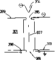
参考图1,粒子束发生器10包括具有提取器孔隙13的提取器极板12,其使用压电控制系统(未示出)定位,使得其位于相对于粒子源14的中心位置。该粒子源是近场纳米尖端源。该纳米尖端是具有约8nm半径的标准SEM尖端。点线的圆环表示提取器极板在横向上可以比标示出来的大很多。加速器镜筒16包括由堆叠形成镜筒的一系列加速极板18,每个极板具有孔隙,该孔被调整成使得当堆叠这些极板时,它们彼此共用共同的纵轴,并且与提取器孔隙13共用共同的纵轴,用以形成延伸的加速孔隙20。每个极板18是彼此电绝缘的,并且可提供有其自身的电压。对于加速电子或者负离子的情况,在右侧示出了极板18上的电压和纳米尖端14上的电压。对于该情况,V总是负的,并且来自该镜筒的电子的最终能量是VT电子伏特(eV)。ΔV是该镜筒中每个极板之间的电压差并且VO是尖端和提取器极板之间的电压差。(最大的负电压在尖端上,并且电压沿该镜筒向下移动而增加直到最终极板上的零电压)。粒子束发生器10可以适于与近场显微镜装置一同使用,并且可被设计用于操作在300~1000eV的能量范围中。调节电极的电压和间隔,使得纳米尖端发射电子,并且加速孔隙中的场是所需用于产生稍微会聚的射束场。电子轨迹示意性地有点线/虚线22表示,其中电子从图中的顶部行进至基部。这些轨迹表示由包络线所限定的整个粒子束分布,其包含从尖端发射并且通过加速器镜筒的电子中的大部分。Referring to FIG. 1 , a particle beam generator 10 includes an extractor plate 12 having an extractor aperture 13 positioned such that it is centrally located relative to a particle source 14 using a piezoelectric control system (not shown). The particle source is a near-field nanotip source. The nanotip is a standard SEM tip with a radius of about 8 nm. The dotted circle indicates that the extractor plate can be much larger laterally than indicated. The accelerator column 16 comprises a series of accelerating plates 18 stacked to form the column, each plate having an aperture adjusted so that when the plates are stacked they share a common longitudinal axis with each other and are connected to the extractor. Apertures 13 share a common longitudinal axis for forming extended acceleration apertures 20 . Each plate 18 is electrically isolated from each other and can be supplied with its own voltage. For the case of accelerated electrons or negative ions, the voltage on the plate 18 and the voltage on the nanotip 14 are shown on the right. For this case, V is always negative, and the resulting energy of electrons from the column is VT electron volts (eV). ΔV is the voltage difference between each plate in the column and VO is the voltage difference between the tip and extractor plates. (The most negative voltage is on the tip and the voltage increases moving down the barrel until zero voltage on the final plate). Particle beam generator 10 may be adapted for use with near-field microscopy arrangements and may be designed to operate in the energy range of 300-1000 eV. The voltage and spacing of the electrodes are adjusted so that the nanotip emits electrons and the accelerating field in the aperture is required to generate a slightly convergent beam field. Electron trajectories are schematically represented by dotted/dotted lines 22, where electrons travel from the top to the base of the figure. These trajectories represent the overall particle beam distribution defined by the envelope that contains the majority of electrons emitted from the tip and passed through the accelerator column.
参考图2,示出的第一级聚焦装置24包括第一微米级透镜系统。安置该微米级透镜系统以收集和聚焦来自加速器孔隙22的粒子束。图2示出了在射束分布26上的聚焦作用。该透镜是像差校正圆柱形单透镜,其包括三个圆柱形元件28、30和32。外面的两个元件28和32处于地电位,而中间的元件提供有足够使电子聚焦在所需位置的电压。(可以施加任何极性的电压,但是当用于聚焦电子时,对于正电压而言像差是最小的,而当用于聚焦正电荷离子时,负电压的像差是最小的)。该特定的微米级透镜的近似比例显示在图的顶端。作为示例,在图中粒子束聚焦在样本夹具34a处,其可以横向移动以扫描样本,并且可以沿射束轴的方向移动以调节焦点。通过调节图1和2的截面上的标有x、y、l和t的相关尺寸来校正该透镜中的像差。Referring to FIG. 2, the first stage focusing device 24 is shown comprising a first micron-scale lens system. The microscale lens system is arranged to collect and focus the particle beam from the accelerator aperture 22 . FIG. 2 shows the focusing effect on the beam profile 26 . The lens is an aberration corrected cylindrical singlet comprising three cylindrical elements 28 , 30 and 32 . The outer two elements 28 and 32 are at ground potential, while the middle element is supplied with a voltage sufficient to focus the electrons at the desired location. (Voltages of either polarity can be applied, but aberrations are minimal for positive voltages when used to focus electrons, and minimal for negative voltages when used to focus positively charged ions). The approximate scale of this particular micron-scale lens is shown at the top of the figure. As an example, in the figure the particle beam is focused at the sample holder 34a, which can be moved laterally to scan the sample, and can be moved in the direction of the beam axis to adjust the focus. Aberrations in this lens are corrected by adjusting the relevant dimensions labeled x, y, 1 and t on the cross-sections of FIGS. 1 and 2 .
参考图3,示出的第二级聚焦装置36包括微型单透镜,其包括三个圆柱形元件38、40和42。其与前文所述的透镜基本相同,除了其较之大一千倍,并且将射束26聚焦在距离安置了样本夹具34b的设备末端若干毫米远的点上。如前文所述,通过使用压电控制系统横向移动样本来实现扫描。而且夹具34b还可以沿轴移动用以将样本安置在正确的焦点处。由于焦距是数毫米,因此在目标上方的空间中放入电子检测器44是可能的。这用于检测和测量反向散射电子,由此可以获得扫描图像。最重要的是,对该透镜进行尽可能的像差校正。除了尺寸a、b、l和t的相关调节,还可以最优化地成形由点线/虚线示出的内表面46的曲率。Referring to FIG. 3 , the second stage focusing device 36 is shown comprising a miniature singlet comprising three cylindrical elements 38 , 40 and 42 . It is essentially the same lens as previously described, except that it is a thousand times larger and focuses the beam 26 to a point a few millimeters away from the end of the apparatus where the sample holder 34b is located. Scanning is achieved by moving the sample laterally using a piezoelectric control system, as previously described. Also the clamp 34b can be moved along the axis to place the sample in the correct focus. Since the focal length is a few millimeters, it is possible to put the electron detector 44 in the space above the target. This is used to detect and measure backscattered electrons, from which scanned images can be obtained. Most importantly, this lens is as aberration corrected as possible. In addition to the relative adjustment of the dimensions a, b, 1 and t, it is also possible to optimally shape the curvature of the inner surface 46 shown by the dotted/broken line.
在使用中,提取器极板置于与粒子源接近的地方,并且在极板和源之间施加了电压,使得通过场发射过程使电子直接从尖端发射。如果如同聚焦离子束源的情况向尖端提供液体金属,则相似的过程还可产生离子束。这些电子/离子束的亮度是极其高的,并且它们因此可以聚焦在小的点上。为了使用该射束并且抑制其横向扩展,使用了具有纳米级提取器孔隙的提取器极板,其后是在面对该尖端的极板侧面上的高电场区域。这样,电子/离子可以成功地从纳米尖端源中提取出来并通过提取器孔隙,通过使用压电平移器件移动提取器极板,如通常在近场光谱法中所使用的,该提取器孔隙可以与位于纳米尖端源上的中心。使提取器极板相对侧上的电场与面对加速电子/离子的纳米尖端源的侧上的电场相似,并且在同一时刻产生微弱的聚焦作用。通过该孔隙的粒子束的尺寸基本上由孔隙的尺寸确定,并且计算显示,如果孔隙的尺寸约为30nm,则大部分发射自纳米尖端源的电子或者离子可以形成于该粒子束中。In use, the extractor plate is placed in close proximity to the particle source and a voltage is applied between the plate and the source such that electrons are emitted directly from the tip by a field emission process. A similar process can also generate an ion beam if liquid metal is supplied to the tip as is the case with a focused ion beam source. The brightness of these electron/ion beams is extremely high, and they can therefore be focused on small spots. In order to use the beam and suppress its lateral expansion, an extractor plate with nanoscale extractor apertures is used, followed by a high electric field region on the side of the plate facing the tip. In this way, electrons/ions can be successfully extracted from the nanotip source and pass through the extractor aperture by moving the extractor plate using a piezoelectric translation device as commonly used in near-field spectroscopy, which can with the center located on the nanotip source. The electric field on the opposite side of the extractor plate is made to be similar to the electric field on the side facing the nanotip source of accelerated electrons/ions and at the same time a weak focusing effect is produced. The size of the particle beam passing through the aperture is essentially determined by the size of the aperture, and calculations show that most of the electrons or ions emitted from the nanotip source can be formed in the particle beam if the size of the aperture is about 30 nm.
该源的设计与传统上使用的源的不同之处在于,该源使用了优选地位于与尖端相距小于数百纳米的位置的纳米级孔隙。这样电子可以通过微小的孔隙提取,并且可以因此随后限制在与后面透镜轴相接近的小的尺寸中。而且其还意味着,需要更小的电压用以从尖端产生场发射。通过使用具有从提取器孔隙延伸的加速孔隙的纳米级/微米级加速镜筒,可在提取器极板两侧之一上产生近似相等的电场,使得提取器极板能够用作弱透镜。这是除了其(加速孔隙)加速电子/离子的功能以外的功能。这样不允许射束在其通过设备的前进过程中明显地扩展,由于该射束的小尺寸,使得限制了透镜像差的不需要的影响,并且允许使用具有1~1000μm范围的孔隙的圆柱形聚焦透镜(既是静电的也是磁的),其非常有利于从整体上减小设备的尺寸。The source design differs from conventionally used sources in that it uses nanoscale apertures preferably located less than a few hundred nanometers from the tip. In this way electrons can be extracted through tiny apertures and can thus then be confined to a small size close to the axis of the rear lens. And it also means that less voltage is needed to generate field emission from the tip. By using a nano/micro accelerating column with an accelerating aperture extending from the extractor aperture, an approximately equal electric field can be generated on one of the sides of the extractor plate, enabling the extractor plate to act as a weak lens. This is in addition to its (accelerating aperture) function of accelerating electrons/ions. This does not allow the beam to expand appreciably during its progression through the device, limits the unwanted effects of lens aberrations due to the small size of the beam, and allows the use of cylindrical A focusing lens (both electrostatic and magnetic), which is very useful for reducing the overall size of the device.
这允许使用具有微米级(次微型的)和毫米焦距的聚焦透镜。由于这些焦距比传统的电子显微镜小很多,因此可以将粒子束聚焦在更小的尺寸中,同时进行较少的透镜像差校正。This allows the use of focusing lenses with micrometer (submicron) and millimeter focal lengths. Since these focal lengths are much smaller than in conventional electron microscopes, particle beams can be focused in smaller sizes with less correction for lens aberrations.
这些微型的和次微型的设计是作为孤立的设备而操作的,用于上达数Kev的最大值的电子/离子能量,但是它们也可以用作操作于上达并超过100keV的较大传统高能量电子/离子束系统的第一级。These miniature and subminiature designs are operated as stand-alone devices for electron/ion energies up to a maximum of a few Kev, but they can also be used as larger conventional high voltage devices operating up to and beyond 100keV. The first stage of an energetic electron/ion beam system.
来自源加速器镜筒的射束随后通过微米级圆柱形单透镜,该圆柱形单透镜位于使得来自加速器镜筒末端的射束在其到达该透镜之前不会明显扩展的距离。然后,可以使用该透镜将射束聚焦在距离最终透镜元件数微米距离处的一纳米以下的直径。为了获得最小的焦点,通过调节元件的几何特征来对其进行像差校正,如下文所述。The beam from the source accelerator column then passes through a micron-sized cylindrical single lens located at such a distance that the beam from the end of the accelerator column does not expand appreciably before it reaches this lens. This lens can then be used to focus the beam to a diameter of less than one nanometer at a distance of a few micrometers from the final lens element. To achieve minimum focus, the element is aberration-corrected by adjusting its geometry, as described below.
尽管可以将此聚焦的射束点直接用于SEM或者FIB技术,但是如果随后使该射束通过具有几百到数千微米的典型孔直径微型的或者次微型的单透镜,则这一点束是更加实用的。该透镜被安置在离开第一微米透镜的最优化的距离处,使得可以在距离透镜的最终透镜元件末端数毫米的距离处获得最小的射束点。该配置是非常实用的,并且允许插入SEM通常所需要的电子检测器。Although it is possible to use this focused beam spot directly for SEM or FIB techniques, if the beam is then passed through a miniature or subminiature singlet lens with a typical aperture diameter of several hundreds to thousands of microns, the spot beam is more practical. The lens is placed at an optimized distance from the first microlens so that the smallest beam spot can be obtained at a distance of a few millimeters from the end of the final lens element of the lens. This configuration is very practical and allows the insertion of electronic detectors normally required by SEMs.
尽管通过该最终透镜的射束尺寸可以小于几微米,但是仍然需要对像差进行校正(主要是球面像差)以获得最佳的性能。这是通过改变其几何特征来完成的,如下文所述。如果该透镜进行了适当的校正,则可以获得明显小于1nm的聚焦的射束点的尺寸。Although the beam size through this final lens can be smaller than a few microns, it still needs to be corrected for aberrations (mainly spherical aberration) for optimal performance. This is done by altering its geometrical features, as described below. If the lens is properly corrected, focused beam spot sizes significantly smaller than 1 nm can be obtained.
对于本领域的技术人员,应当认识到,可以使用其他的同样适用于本发明工作的第一和第二级聚焦装置。It will be appreciated by those skilled in the art that other primary and secondary focusing arrangements may be used which are equally suitable for the operation of the present invention.
参考图4,示出了完整的系统,其包括两个4元件的圆柱形单透镜、一个是微米级的,标为B,另一个是微型的,标为C。这些透镜位于标为A的电子/离子源的下游。通过对其几何特征进行众多的变化,可以使它们具有非常低的像差。这与相机和光学设备中的多元件光学透镜有些相似。这些射束元件的最终设计取决于电子/射束进入透镜时的电子/射束能量、散度和尺寸。可以改变的参数是:Referring to Figure 4, the complete system is shown, comprising two 4-element cylindrical singlets, one micron scale, labeled B, and the other miniature, labeled C. These lenses are located downstream of the electron/ion source labeled A. They can be made to have very low aberrations by making numerous changes to their geometrical features. This is somewhat similar to multi-element optical lenses in cameras and optical devices. The final design of these beam elements depends on the electron/beam energy, divergence and size of the electron/beam as it enters the lens. The parameters that can be changed are:
1)元件的数量1) Number of components
2)每个电极的厚度2) The thickness of each electrode
3)电极之间的距离3) Distance between electrodes
4)每个电极中的孔隙尺寸4) Pore size in each electrode
5)如前文应用中所示的透镜上的边缘的形状5) The shape of the edge on the lens as shown in the previous application
6)施加给每个电极的电压6) Voltage applied to each electrode
通过适当地改变这些参数,我们几乎能够完全地从我们的系统中除去球面像差。By varying these parameters appropriately, we can almost completely remove spherical aberration from our system.
图4示出了4元件透镜的几何尺寸,其具有标为48、50、52和54的电极,这些电极分别具有电压V1、V2、V3和V4。射束及其方向标为56。第一分析位置58位于离开微米级透镜末端距离为焦距f1的位置。通过使用如扫描隧道显微镜常常使用的压电元件移动样本,实现了射束的扫描。可以移去该样本位置,并且使射束通过第二微型透镜,以便于到达距离第二透镜末端距离为f2的焦点。在该点处存在压电驱动样本夹具60。尽管所示的该第二微型透镜具有与第一透镜相同的几何特征,但是这对于其他情况不是必需的。确切的几何特征(孔隙尺寸等)将再次取决于射束通过该透镜时的特征。典型的孔隙尺寸是约5μm(对于微米级透镜)和5mm(对于微型透镜),但是这些可以在宽的范围中变化。Figure 4 shows the geometry of a 4-element lens with electrodes labeled 48, 50, 52 and 54 having voltages Vl, V2, V3 and V4, respectively. The beam and its direction are designated 56 . The first analysis position 58 is located at a distance of the focal length f1 away from the end of the micron-scale lens. The scanning of the beam is achieved by moving the sample using a piezoelectric element as is often used in scanning tunneling microscopes. The sample position can be removed and the beam passed through a second microlens in order to reach a focal point at a distance f2 from the end of the second lens. At this point there is a piezo-driven sample holder 60 . Although this second microlens is shown to have the same geometrical characteristics as the first lens, this is not necessary for other cases. The exact geometry (aperture size, etc.) will again depend on the characteristics of the beam as it passes through the lens. Typical aperture sizes are around 5 μm (for microlenses) and 5 mm (for microlenses), but these can vary within wide ranges.
在图5中示出了本发明的另一实施例,其中粒子束发生器是微芯片100,其包括一个或者多个产生窄的(<50nm)轴上射束的纳米镜筒162。纳米尖端114位于该微米结构的末端,其连结到垂直悬臂(未示出)上并在中心安置,并且离开纳米镜筒162的第一孔隙13的距离大于10nm。纳米镜筒162可以是所示的一个或者多个部分,并且限定了具有小于50nm横向尺寸的轴向射束。在图5b中示出了典型的纳米镜筒162,并且其由薄的多层膜制成,该多层膜包括交替的金属(导电)层118,中间间隔有绝缘层119,其中通过光刻技术或者使用聚焦离子束(FIB)“研磨机”使孔隙13穿过该纳米镜筒162。该纳米镜筒的总长度可以上达2μm,并且足够用于准确地确定(轴上)方向和射束发射度的相空间。如所示出的,纳米尖端114位于该孔隙上面,并且在尖端114和纳米镜筒电极162之间施加有电压差。由纳米镜筒限定的射束具有轴164,其与多元件的微米级单透镜是同心的。该透镜包括金属(导电)电极166,其中间间隔有绝缘体168。所示的组件包括四个中间间隔有绝缘体的金属电极并且位于距离纳米镜筒仅有几个微米的位置,其被作为微米透镜的具有相同尺寸的孔隙的绝缘膜与该纳米镜筒隔开。在前文的应用中给出了关于该透镜的适当的孔隙直径。增加叠层中金属导电电极的数目可以减小该透镜中的像差。Another embodiment of the invention is shown in FIG. 5, wherein the particle beam generator is a
图6示出了一种方法,用于构造显微镜使得微米透镜可以将射束聚焦在离开设备末端小于50μm距离的点处。如果该射束具有小于1nm并且接近1的横向尺寸时,该条件是必需的。(该射束点基本上确定了设备的分辨率)。在图6b的近场显微镜方法中示出了本发明的该实施例的应用,并且其包括刚性连结于近场显微镜的水平悬臂170的“芯片”或者体100,其可以使用标准的纳米定位技术进行定位。在此之上的垂直悬臂固定了纳米尖端114,并且其可以垂直移动并在水平面上进行扫描。样本安装在特殊的固定器172上,该固定器172具有用于连结样本的小的表面面积。(该原子分辨率配置仅可用于小面积的样本;对于较大的面积,增大微米透镜的焦距,并且分辨率下降至约1nm)。显微镜主体下方的另外的垂直悬臂174固定了样本固定器,并且提供将样本定位在正确的垂直距离处定位以及在水平面中进行扫描的手段。Figure 6 shows a method for constructing a microscope such that microlenses can focus the beam to a point at a distance less than 50 μm from the end of the device. This condition is necessary if the beam has a lateral dimension of less than 1 nm and close to 1 Å. (The beam spot basically determines the resolution of the device). The application of this embodiment of the invention is shown in the near-field microscopy approach of Figure 6b, and comprises a "chip" or
在图6a中示出了体或芯片100的细节。通过光刻技术或利用激光射束进行微米机器加工在该芯片的一个边缘产生了一系列台阶。基部的台阶仅有几个μm厚并且宽于约20μm。在该台阶176上形成了多层组件178,其基本上是如图6a所示的粒子束发生器的主体。该多个层是通过两个阶段中的原子淀积生长的。首先产生对应于静电透镜的层,并且通过光刻技术在位于对应于图中由字母A标出的台阶边缘附近的层中制造对应于透镜孔的孔113。(可以在一个光刻制程中产生多个孔,并且每个都可以是分立的显微镜)。顶层由1纳米厚的金膜或者碳膜覆盖,并且随后(通过原子淀积)生长对应于纳米镜筒层的连续的多个层。该层是使用水平掩膜产生的,其允许每个分立的层终止于沿台阶的不同位置。这提供了将电气接触连结到显微镜中的电极的基本方法,如曝光区域180所示。最后,使用聚焦离子束,在带有静电透镜的轴上钻该通过顶部多个层的纳米镜筒孔。(这还可以通过现有技术的电子束光刻技术和干蚀刻技术完成)。A detail of the body or
在操作中,纳米尖端114位于孔隙的中心,并且调节透镜上的电压以通过轴164将射束聚焦到焦点182处的样本上。设置支撑台阶176的厚度和焦距,使得存在足够大的间隙,用以通过通道倍增器184记录反向散射电子。In operation, the
两个另外的调整可用于允许显微镜包含于单个的芯片中。首先可以在芯片的体中制造纳米尖端和显微镜悬臂。(这可能是水平悬臂)。其次可以将探测器制造在该芯片的基部。为了该目的,最好是使用用于电子的半导电雪崩型检测器。甚至可以考虑在该芯片的基部并入用于扫描样本的机构,用以在芯片上制造最终的SEM。Two additional adjustments are available to allow the microscope to be contained on a single chip. First, nanotips and microscope cantilevers can be fabricated in the bulk of the chip. (this may be a horizontal cantilever). Second, detectors can be fabricated at the base of the chip. For this purpose, it is preferable to use a semiconducting avalanche type detector for electrons. It is even conceivable to incorporate a mechanism for scanning the sample at the base of the chip for making the final SEM on the chip.
在使用中,典型的尺寸和电压与上文所述的关于本发明的前面的实施例的尺寸和电压相同。对纳米尖端114来说一种合适的配置是使用如扫描隧道显微镜(STM)中所使用的垂直悬臂配置进行定位。然而,近来光刻的发展使得可以将该悬臂并入到显微镜本身中。纳米镜筒包括具有导电(金属或者硅)薄膜的多个层,其由绝缘层隔开,穿过该层制造了具有所需纳米级(典型地小于50nm)的圆孔。这是通过光刻技术或者通过使用聚焦离子束的钻孔方法来完成的。微米级的多元件单透镜位于纳米镜筒下面并且与之同心。这可以作为分立的部分而制成,并且可以使用标准的微米定位系统使之独立地相对于纳米镜筒进行定位。在较简单的形式中,微米透镜被制成与纳米镜筒相同的多层结构,并且其整体形成了显微镜的基本元件。透镜的制造可以通过多种技术来完成,其包括光刻和激光束机器加工。In use, typical dimensions and voltages are the same as those described above in relation to the previous embodiments of the invention. One suitable configuration for the
显微镜主体固定在垂直臂(悬臂)上,其可以定位成垂直和横向。通过伺服机构使纳米探针位于纳米镜筒孔隙的中心上,该伺服机构使用扇形金属薄膜中的电流,而该扇形金属薄膜形成了纳米镜筒中的第一电极。在显微镜主体下是位于垂直悬臂末端上的样本镜台。电子束聚焦在该样本上,并且通过使用如STM中使用的标准纳米定位技术(例如使用压电机构)移动悬臂的末端,可以使电子束沿样本移动。如果使用电子检测器(通道倍增器)检测到反向散射电子,则可以制成原表面子结构的图像。在最终的设计中,电子检测器可以并入到显微镜芯片的基部。The microscope body is fixed on a vertical arm (cantilever), which can be positioned vertically and laterally. The nanoprobe is positioned over the center of the nanocolumn aperture by a servo mechanism that uses an electric current in the fan-shaped metal film that forms the first electrode in the nanocolumn. Below the microscope body is the sample stage on the end of the vertical cantilever. The electron beam is focused on the sample and can be moved along the sample by moving the end of the cantilever using standard nanopositioning techniques as used in STM (eg using a piezoelectric mechanism). If the backscattered electrons are detected using an electron detector (channel multiplier), an image of the substructure of the original surface can be made. In the final design, electron detectors can be incorporated into the base of the microscope chip.
使用前面的描述,通过使液体镓流入纳米尖端并且翻转电压的极性,可以调整适用于机器加工低于10nm的表面结构的聚焦离子束系统的设计。在该配置中,其几何形状是倒转的,使得纳米尖端位于纳米镜筒下面。(这是用于防止液体镓污染显微镜)。Using the previous description, by flowing liquid gallium into the nanotip and flipping the polarity of the voltage, the design of a focused ion beam system suitable for machining sub-10 nm surface structures can be tuned. In this configuration, its geometry is inverted so that the nanotip is located below the nanotube. (This is used to prevent liquid gallium from contaminating the microscope).
在图7和8中示出了本发明的另外的实施例,其中粒子束发生器200包括一对薄膜金属层212和213,其由半导体材料284隔开。每个金属层包括校准孔隙286和288(纳米校准器)。粒子束发生器200还包括加速孔隙220,其延伸通过半导体层材料,并且与校准孔隙286和288共有一个纵轴。加速孔隙220的直径大于校准孔隙286和288每一个的直径。典型地,加速孔隙的直径可以是约50nm,而纳米校准器孔隙是约30nm。如果有足够的电压差存在于尖端和校准孔隙286之间,则粒子将从纳米尖端214发射。如果跨接在该半导体的电压差足够高,则这些粒子将被加速并且被聚焦在几乎平行的射束中。(在图7a和7b中箭头290示出了电子束的方向)。典型地,对于0.5μm的硅薄晶片或者膜,跨接在该半导体的电压可以是约300伏特,并且这将沿孔产生600MV/m的均匀场。如果纳米镜筒以图7b所示的两级形式制造,则较长的纳米镜筒是可能的。这里,有两个被导电膜213隔开的层。底部层285是导电的,并且可以由金属制造或者优选地由具有非常低电阻率的掺杂硅制造。如果两个金属薄膜213和214处于地电位,则整个底部镜筒285也处于地电位。纳米孔隙286执行与图7a中所示器件相同的功能,但是可以距离纳米尖端几微米的孔隙288能够减小散射,同时进一步降低(相空间)电子束发射度。此下面的镜筒285中的孔与上面加速部分的孔在同一时间制造。其唯一的功能是支撑纳米孔隙288与半导体中的孔同心。限制于孔隙尺寸288的直径的窄的电子束随后到达显微镜的静电聚焦元件,如图8所示。A further embodiment of the invention is shown in FIGS. 7 and 8 , wherein the particle beam generator 200 includes a pair of thin film metal layers 212 and 213 separated by a semiconductor material 284 . Each metal layer includes
在图8中示出了用作显微镜的完整的粒子束发生器系统,其中纳米镜筒290中有孔,并且纳米尖端214是电子源。如所示出的,窄的电子束222通过纳米镜筒286/288并且通过同心的单透镜。该透镜是简单的三元件配置,其由分别是导电层和绝缘层的292和294制成,穿过其中制造了孔隙。包含5个或者更多的电极的多元件透镜还可以用于减小前面关于其他实施例而提及的像差。选择电极的内径(透镜的孔隙)和间距以给出最小的像差并且因而给出最小的射束点。该透镜的内径的典型尺寸是约2μm,并且每个层是约1μm厚。如果单透镜由具有三个分立层的单个薄晶片制成,则其制造过程可以简化。使用具有不同掺杂浓度的硅可以制造导电层292和绝缘层294。对于简单的3元件透镜,外部的两个导电电极处于地电位,而中间的一个处于正确的电位,用以在距离组件296末端的所需距离处给出焦点。该完整的组件形成了显微镜主体,并且当其是在阶梯状组件的边缘制造时,如前文在另一实施例中提及的,射束发生器基本上是远离纳米尖端的单个芯片。然而,该纳米尖端位于悬臂的末端,使得可以将其定位在纳米镜筒入口孔隙的中心,并且因此可以整体到纳米芯片中以获得完整的聚焦电子(离子)束机械,称为“片上显微镜”。应当注意,制成显微镜主体的电阻性膜可以在其中具有很多孔,使得通过将纳米探针移动到任何入口孔隙,可以进入其中。A complete particle beam generator system for use as a microscope is shown in FIG. 8 with the nanocolumn 290 having a hole in it and the nanotip 214 as the source of electrons. As shown, the narrow electron beam 222 passes through the
在前面的实施例中,加速纳米镜筒由具有交替的金属(导电)和绝缘层的多层结构构建而成,其中穿过该结构制造了具有小于100nm直径的孔,并且其是电子通过的通道。通过对该组件中的导电电极施加电压,可以产生沿该镜筒中真空孔隙的高电场。本实施例是产生纳米镜筒或者加速器的较简单的方法,其对前面的组件具有相同的作用。而且,此新器件便于制造,并且可以适用于在该镜筒两端包括限制(抗散射)校准器的场合。该方法是使用微米制造技术从单个高电阻率材料片(穿过该材料片制造了孔)制造加速器。尽管不是唯一可能的,但理想的材料是单晶掺杂硅,如微芯片制造中所使用的。掺杂通常是n型的(尽管p型也是可以的),并且掺杂密度应是使电阻率在1kΩm-cm~100MΩm-cm的范围中,但这不是唯一的。所施加的跨接在该材料的薄膜的电压将确保沿任何通过该电阻性材料的直孔均存在均匀的电场。该孔被制造为垂直于薄晶片或者薄膜的平行侧,该薄晶片或者薄膜是加速器的主体,并且可被宽泛地称为纳米镜筒,符合前面关于由具有交替的绝缘薄膜和导电薄膜的多层构建的镜筒的术语。(使用了纳米镜筒是因为通过该膜的孔隙处于纳米尺度范围中)。在该情况中,电场是沿(真空)孔方向的,并且因而其可以对注入到该孔中的电子进行加速。如果尖端上的电压超过表面电压约10伏特,则可被定位在具有典型的50nm孔隙的孔上方约30nm距离处的纳米尖端将场发射电子。半导体的两个表面覆盖有薄的金属膜,穿过该金属膜制造了与半导体中的孔同心的孔。金属膜中孔的直径小于半导体中孔的直径,使得这些孔隙用作抗散射校准器,并且还可以用于减少电子束发射度。In the previous example, the accelerating nanocolumn was built from a multilayer structure with alternating metallic (conducting) and insulating layers through which holes were made with a diameter of less than 100 nm and through which electrons passed. aisle. By applying a voltage to the conductive electrodes in the assembly, a high electric field can be generated along the vacuum aperture in the column. This embodiment is a simpler way to create a nanocolumn or accelerator that does the same thing as the previous components. Furthermore, the new device is easy to manufacture and can be adapted to include limiting (anti-scatter) collimators at both ends of the column. The method is to fabricate the accelerator from a single sheet of high-resistivity material through which holes are made, using microfabrication techniques. Although not the only possibility, the ideal material is single crystal doped silicon, as used in microchip manufacturing. The doping is usually n-type (although p-type is also possible), and the doping density should be such that the resistivity is in the range of 1 kΩm-cm to 100 MΩm-cm, but this is not exclusive. The applied voltage across the thin film of the material will ensure that a uniform electric field exists along any straight hole through the resistive material. The aperture is fabricated perpendicular to the parallel sides of the thin wafer or membrane that is the bulk of the accelerator and can be broadly referred to as a nanotube, in line with the previous discussion of a multi-column with alternating insulating and conducting films. A term for barrels built in layers. (Nanocolumns are used because the pores through the membrane are in the nanoscale range). In this case the electric field is in the direction of the (vacuum) hole and thus it can accelerate electrons injected into the hole. A nanotip, which can be positioned at a distance of about 30 nm above a hole with a typical 50 nm aperture, will field emit electrons if the voltage on the tip exceeds the surface voltage by about 10 volts. Both surfaces of the semiconductor are covered with a thin metal film through which a hole is made concentric to the hole in the semiconductor. The diameter of the pores in the metal film is smaller than the diameter of the pores in the semiconductor, so that these pores act as anti-scatter collimators and can also be used to reduce electron beam emittance.
处于聚焦电子中的这些纳米镜筒和射束器件的操作如下。向最接近纳米探针的金属层施加负电压,并且向纳米尖端施加较大的负电压。在另一半导体表面上的金属层处于地电位。通过正确地选择这些电压,从尖端发射的电子可被聚焦并且被加速到达在纳米镜筒的孔。可以产生具有小于50nm直径的几乎平行的电子束。The operation of these nanocolumns and beam devices in focused electrons is as follows. A negative voltage is applied to the metal layer closest to the nanoprobe, and a larger negative voltage is applied to the nanotip. The metal layer on the other semiconductor surface is at ground potential. By choosing these voltages correctly, electrons emitted from the tip can be focused and accelerated to reach the hole in the nanocolumn. Nearly parallel electron beams with a diameter of less than 50 nm can be generated.
为了获得最佳的性能,校准器孔隙的直径需要小于100nm,并且硅的厚度大于0.5μm。如果该配置有效,则重要的是,器件包括校准器以减小由(纳米级孔的)壁引起的散射并且还减小射束的总发射度。后者是非常重要的,这是因为射束的总发射度与最终的射束点尺寸成比例。因此通过使用仔细挑选的校准器所引起的发射度的大的降低可以导致最终射束点尺寸的明显减少。两种方法可用于制造纳米级的校准器。在第一种方法中,纳米级的镜筒在其中具有圆锥形的孔,且较小直径的孔位于最接近纳米尖端电子源。在该方法中,可以极大地消除由孔的内壁引起的电子束的散射。圆锥的形状可以由这样的形式替换,其中在需要校准的位置更加突然地减小孔的孔隙。这些校准器在需要时可以形成在管的两个末端。在另一种方案中,在孔的一个末端或两个末端处离子蚀刻薄的金属覆盖层,用以产生校准器。这可以通过干蚀刻技术完成,或者可以通过使用聚焦离子束(FIB)研磨机来完成。For optimal performance, the diameter of the etalon pores needs to be less than 100 nm and the silicon thickness to be greater than 0.5 μm. If this configuration is to be effective, it is important that the device includes collimators to reduce scattering by the walls (of the nanoscale aperture) and also reduce the overall emittance of the beam. The latter is very important because the total emittance of the beam is proportional to the final beam spot size. Thus a large reduction in emittance induced by the use of a carefully chosen collimator can lead to a significant reduction in the final beam spot size. Two methods can be used to fabricate calibrator at the nanoscale. In the first method, the nanoscale column has a conical hole in it, and the smaller diameter hole is located closest to the nanotip electron source. In this method, the scattering of electron beams caused by the inner wall of the hole can be largely eliminated. The conical shape can be replaced by a form in which the porosity of the hole is reduced more abruptly where calibration is required. These calibrators can be formed at both ends of the tube if desired. In another approach, a thin metal capping layer is ion etched at one or both ends of the hole to create the etalon. This can be done by dry etching techniques, or it can be done by using a focused ion beam (FIB) mill.
在图9中示出了一般的配置,其中电子源是位于器件第一纳米级部分入口处的纳米尖端314,其中标出了射束方向390。图9a示出了具有微米厚度的材料部分301,穿过该材料通过干蚀刻技术制造了50nm(典型尺寸)的圆孔。如果仔细控制蚀刻可以使该孔的壁平行。整个的显微镜镜筒或组件可以由加速部分和非加速部分构成,如前面实施例中所描述的。制造这些孔隙286和288的一种方法如下。在产生孔的过程中,在表面上产生配准特征398以绘出孔隙的位置。然后在该表面上通过真空淀积技术(从源进行原子淀积)涂敷纳米厚度的金层,并且2~3nm(典型的)厚的金箔312和313安置在该第一层顶部上的孔隙上。(如果这是在洁净条件下完成的,则金箔将接合至硅上的真空淀积的金层)。然后可以在该金属箔上通过射束钻孔或者干蚀刻产生孔隙286和288。(为了使之可能,重要的是在粘附金层之后,配准部分是保持可见的)。图9b示出了特别是在加速部分入口处产生孔隙的可替换的方法。在该方法中,该孔锥形式变细成为所示的圆锥形。通过仔细地控制干蚀刻工艺,可以产生该锥形式变细的形状。然后,通过使用标准的真空淀积方法在表面上淀积金属,制成顶部导电层399。通过前面的方法制造的另外的孔隙可以安置在该组件下面,如中间的图所示。然而,同样可以的是,通过将在其中具有锥形式变细的孔的第二晶片安置在中间图中所示的晶片的下面,在该位置处产生校准器。于是这取代了由薄膜金属(金)制成的孔隙。其可以制造在分立的薄(硅)晶片中,该晶片被定位为使得该孔是同心的或者使得在一个区域上制造整个组件。这样,系统现在有效地包括两个具有圆锥形孔的晶片,其中该两个晶片都涂敷在它们具有金属膜的平坦侧上。同样可以的是,通过晶片的本征材料制造校准器而不必采用锥形式变细的形式,如图9c所示。可以在一个或多个组件(晶片)的一个末端或者两个末端制造校准器。可以堆叠这些校准器以使散射最小化和/或减少射束的相空间发射度。A general configuration is shown in Figure 9, where the electron source is a
Claims (17)
Applications Claiming Priority (10)
| Application Number | Priority Date | Filing Date | Title |
|---|---|---|---|
| GB0213772.7 | 2002-06-15 | ||
| GB0213772A GB0213772D0 (en) | 2002-06-15 | 2002-06-15 | Focussed electron and ion Beams |
| GB0219818.2 | 2002-08-24 | ||
| GB0219818A GB0219818D0 (en) | 2002-08-24 | 2002-08-24 | Focussed electron and ion beams addendum |
| GB0300265A GB0300265D0 (en) | 2003-01-07 | 2003-01-07 | Focussed electron and ion beams-part2 |
| GB0300265.6 | 2003-01-07 | ||
| GB0302591.3 | 2003-02-05 | ||
| GB0302591A GB0302591D0 (en) | 2003-02-05 | 2003-02-05 | A nanoaccelerator for focussed electron and ion beam machines |
| GB0303402.2 | 2003-02-14 | ||
| GB0303402A GB0303402D0 (en) | 2003-02-05 | 2003-02-14 | Nanoscale collimators for focussed electron and ion beam machines |
Publications (2)
| Publication Number | Publication Date |
|---|---|
| CN1663013A true CN1663013A (en) | 2005-08-31 |
| CN100359626C CN100359626C (en) | 2008-01-02 |
Family
ID=29741081
Family Applications (1)
| Application Number | Title | Priority Date | Filing Date |
|---|---|---|---|
| CNB038139146A Expired - Fee Related CN100359626C (en) | 2002-06-15 | 2003-06-16 | particle beam generator |
Country Status (8)
| Country | Link |
|---|---|
| US (1) | US7109493B2 (en) |
| EP (1) | EP1532649A2 (en) |
| JP (1) | JP4392346B2 (en) |
| CN (1) | CN100359626C (en) |
| AU (1) | AU2003253085B2 (en) |
| CA (1) | CA2492835A1 (en) |
| NZ (1) | NZ537145A (en) |
| WO (1) | WO2003107375A2 (en) |
Cited By (7)
| Publication number | Priority date | Publication date | Assignee | Title |
|---|---|---|---|---|
| CN101026080B (en) * | 2006-02-22 | 2010-04-21 | Fei公司 | Particle-optical apparatus equipped with a gas ion source |
| CN105321790A (en) * | 2014-05-26 | 2016-02-10 | 斯伊恩股份有限公司 | Ion implantation apparatus |
| CN105874559A (en) * | 2013-11-14 | 2016-08-17 | 迈普尔平版印刷Ip有限公司 | Multi-Electrode Electron Optical System |
| CN106328478A (en) * | 2016-10-27 | 2017-01-11 | 中国科学院武汉物理与数学研究所 | Device for generating low-energy ions |
| US11094426B2 (en) | 2012-05-14 | 2021-08-17 | Asml Netherlands B.V. | Vacuum chamber arrangement for charged particle beam generator |
| US11348756B2 (en) | 2012-05-14 | 2022-05-31 | Asml Netherlands B.V. | Aberration correction in charged particle system |
| CN115295382A (en) * | 2022-08-09 | 2022-11-04 | 中国科学院近代物理研究所 | Self-adaptive ion beam correction deflection plate |
Families Citing this family (24)
| Publication number | Priority date | Publication date | Assignee | Title |
|---|---|---|---|---|
| DE602004031817D1 (en) * | 2004-01-21 | 2011-04-28 | Integrated Circuit Testing | Radiation-optical component with a particle-optical lens |
| US8003934B2 (en) * | 2004-02-23 | 2011-08-23 | Andreas Hieke | Methods and apparatus for ion sources, ion control and ion measurement for macromolecules |
| US20050194543A1 (en) * | 2004-02-23 | 2005-09-08 | Ciphergen Biosystems, Inc. | Methods and apparatus for controlling ion current in an ion transmission device |
| CA2604820A1 (en) * | 2004-02-23 | 2005-09-09 | Gemio Technologies, Inc. | Ion source with controlled superposition of electrostatic and gas flow fields |
| JP2009505368A (en) * | 2005-08-18 | 2009-02-05 | シーイービーティー・カンパニー・リミティッド | Electron beam energy conversion method for electron column |
| CN102103966B (en) * | 2005-11-28 | 2013-02-06 | 卡尔蔡司Smt有限责任公司 | Particle-optical component |
| KR101384260B1 (en) * | 2005-12-05 | 2014-04-11 | 전자빔기술센터 주식회사 | Method for focusing electron beam in electron column |
| US7883839B2 (en) * | 2005-12-08 | 2011-02-08 | University Of Houston | Method and apparatus for nano-pantography |
| FR2897719B1 (en) * | 2006-02-20 | 2008-10-03 | Centre Nat Rech Scient | NANO-MANUFACTURING INSTALLATION AND METHOD |
| JP2010517233A (en) * | 2007-01-25 | 2010-05-20 | エヌエフエイビー・リミテッド | Improved particle beam generator |
| US8642959B2 (en) * | 2007-10-29 | 2014-02-04 | Micron Technology, Inc. | Method and system of performing three-dimensional imaging using an electron microscope |
| US8638109B2 (en) * | 2009-12-31 | 2014-01-28 | Mapper Lithography Ip B.V. | Capacitive sensing system with differential pairs |
| GB201000952D0 (en) | 2010-01-21 | 2010-03-10 | Nfab Ltd | A sub miniature low energy scanned beam microscope |
| DE102010041156B9 (en) | 2010-09-21 | 2018-01-25 | Carl Zeiss Microscopy Gmbh | Aperture unit for a particle beam device and particle beam device |
| US20120027946A1 (en) * | 2010-11-19 | 2012-02-02 | Steele Adam V | Direct deposit and removal of nanoscale conductors |
| JP5744579B2 (en) * | 2011-03-15 | 2015-07-08 | キヤノン株式会社 | Charged particle beam lens and exposure apparatus using the same |
| JP5669636B2 (en) * | 2011-03-15 | 2015-02-12 | キヤノン株式会社 | Charged particle beam lens and exposure apparatus using the same |
| US8674321B2 (en) * | 2012-02-28 | 2014-03-18 | Tiza Lab, L.L.C. | Microplasma ion source for focused ion beam applications |
| GB201207881D0 (en) * | 2012-05-04 | 2012-06-20 | Isis Innovation | Active chemical sensing using optical microcavity |
| CN107359101B (en) * | 2012-05-14 | 2019-07-12 | Asml荷兰有限公司 | High voltage shielded and cooling in beam of charged particles generator |
| WO2014185060A1 (en) * | 2013-05-13 | 2014-11-20 | 国立大学法人神戸大学 | Charged particle optical lens device and charged particle optical lens device control method |
| CN105225918B (en) * | 2014-06-13 | 2017-04-05 | 中国科学院大连化学物理研究所 | For the electrostatic lenses of flight time mass spectrum intermediate ion beam shaping |
| KR20160102588A (en) * | 2015-02-20 | 2016-08-31 | 선문대학교 산학협력단 | Micro-electron column having an electron emitter improving the density of an electron beam emitted from a nano structure tip |
| US11508591B2 (en) * | 2021-02-08 | 2022-11-22 | Kla Corporation | High resolution electron beam apparatus with dual-aperture schemes |
Family Cites Families (6)
| Publication number | Priority date | Publication date | Assignee | Title |
|---|---|---|---|---|
| JPH11250850A (en) * | 1998-03-02 | 1999-09-17 | Hitachi Ltd | Scanning electron microscope, microscope method, and interactive input device |
| US6023060A (en) * | 1998-03-03 | 2000-02-08 | Etec Systems, Inc. | T-shaped electron-beam microcolumn as a general purpose scanning electron microscope |
| US6281508B1 (en) * | 1999-02-08 | 2001-08-28 | Etec Systems, Inc. | Precision alignment and assembly of microlenses and microcolumns |
| US6369385B1 (en) * | 1999-05-05 | 2002-04-09 | Applied Materials, Inc. | Integrated microcolumn and scanning probe microscope arrays |
| US6787772B2 (en) * | 2000-01-25 | 2004-09-07 | Hitachi, Ltd. | Scanning electron microscope |
| EP1439566B1 (en) * | 2003-01-17 | 2019-08-28 | ICT, Integrated Circuit Testing Gesellschaft für Halbleiterprüftechnik mbH | Charged particle beam apparatus and method for operating the same |
-
2003
- 2003-06-16 EP EP03760078A patent/EP1532649A2/en not_active Withdrawn
- 2003-06-16 JP JP2004514103A patent/JP4392346B2/en not_active Expired - Fee Related
- 2003-06-16 AU AU2003253085A patent/AU2003253085B2/en not_active Ceased
- 2003-06-16 WO PCT/GB2003/002560 patent/WO2003107375A2/en not_active Ceased
- 2003-06-16 US US10/518,064 patent/US7109493B2/en not_active Expired - Fee Related
- 2003-06-16 NZ NZ537145A patent/NZ537145A/en not_active IP Right Cessation
- 2003-06-16 CA CA002492835A patent/CA2492835A1/en not_active Abandoned
- 2003-06-16 CN CNB038139146A patent/CN100359626C/en not_active Expired - Fee Related
Cited By (18)
| Publication number | Priority date | Publication date | Assignee | Title |
|---|---|---|---|---|
| CN101026080B (en) * | 2006-02-22 | 2010-04-21 | Fei公司 | Particle-optical apparatus equipped with a gas ion source |
| US11094426B2 (en) | 2012-05-14 | 2021-08-17 | Asml Netherlands B.V. | Vacuum chamber arrangement for charged particle beam generator |
| US12387903B2 (en) | 2012-05-14 | 2025-08-12 | Asml Netherlands B.V. | Aberration correction in charged particle system |
| US11961627B2 (en) | 2012-05-14 | 2024-04-16 | Asml Netherlands B.V. | Vacuum chamber arrangement for charged particle beam generator |
| US11705252B2 (en) | 2012-05-14 | 2023-07-18 | Asml Netherlands B.V. | Vacuum chamber arrangement for charged particle beam generator |
| US11348756B2 (en) | 2012-05-14 | 2022-05-31 | Asml Netherlands B.V. | Aberration correction in charged particle system |
| CN109637921B (en) * | 2013-11-14 | 2021-10-26 | Asml荷兰有限公司 | Multi-electrode electron optical system |
| CN105874559B (en) * | 2013-11-14 | 2018-11-23 | 迈普尔平版印刷Ip有限公司 | Multi-Electrode Electron Optical System |
| CN109637921A (en) * | 2013-11-14 | 2019-04-16 | 迈普尔平版印刷Ip有限公司 | Multi-electrode electron-optical system |
| CN107507750B (en) * | 2013-11-14 | 2020-02-07 | Asml荷兰有限公司 | Multi-electrode stack arrangement |
| CN107507750A (en) * | 2013-11-14 | 2017-12-22 | 迈普尔平版印刷Ip有限公司 | Multi-electrode stacked arrangement |
| CN105874556B (en) * | 2013-11-14 | 2017-12-12 | 迈普尔平版印刷Ip有限公司 | Multi-electrode stack arrangement |
| CN105874556A (en) * | 2013-11-14 | 2016-08-17 | 迈普尔平版印刷Ip有限公司 | Multi-electrode stack arrangement |
| CN105874559A (en) * | 2013-11-14 | 2016-08-17 | 迈普尔平版印刷Ip有限公司 | Multi-Electrode Electron Optical System |
| CN105321790B (en) * | 2014-05-26 | 2018-01-16 | 斯伊恩股份有限公司 | Ion implantation apparatus |
| CN105321790A (en) * | 2014-05-26 | 2016-02-10 | 斯伊恩股份有限公司 | Ion implantation apparatus |
| CN106328478A (en) * | 2016-10-27 | 2017-01-11 | 中国科学院武汉物理与数学研究所 | Device for generating low-energy ions |
| CN115295382A (en) * | 2022-08-09 | 2022-11-04 | 中国科学院近代物理研究所 | Self-adaptive ion beam correction deflection plate |
Also Published As
| Publication number | Publication date |
|---|---|
| CA2492835A1 (en) | 2003-12-24 |
| US20050199820A1 (en) | 2005-09-15 |
| NZ537145A (en) | 2006-09-29 |
| US7109493B2 (en) | 2006-09-19 |
| WO2003107375A3 (en) | 2004-03-04 |
| JP2005530314A (en) | 2005-10-06 |
| JP4392346B2 (en) | 2009-12-24 |
| WO2003107375A2 (en) | 2003-12-24 |
| AU2003253085A1 (en) | 2003-12-31 |
| EP1532649A2 (en) | 2005-05-25 |
| AU2003253085B2 (en) | 2008-11-20 |
| CN100359626C (en) | 2008-01-02 |
Similar Documents
| Publication | Publication Date | Title |
|---|---|---|
| CN100359626C (en) | particle beam generator | |
| JP6905555B2 (en) | Charged particle beam devices, multi-beam blankers for charged particle beam devices, and methods for operating charged particle beam devices | |
| JP6845900B2 (en) | Charged particle beam devices, multi-beam blankers for charged particle beam devices, and methods for operating charged particle beam devices | |
| US20170309438A1 (en) | Electrostatic lens structure | |
| US6771012B2 (en) | Apparatus for producing a flux of charge carriers | |
| US9754759B2 (en) | Electrostatic multipole device, electrostatic multipole arrangement, and method of manufacturing an electrostatic multipole device | |
| US20100187433A1 (en) | Improved particle beam generator | |
| Kratschmer et al. | Sub‐40 nm resolution 1 keV scanning tunneling microscope field‐emission microcolumn | |
| EP0731981B1 (en) | Particle-optical apparatus comprising an electron source with a needle and a membrane-like extraction electrode | |
| EP2023372B1 (en) | Electrostatic Lens Unit | |
| US11615938B2 (en) | High-resolution multiple beam source | |
| Muray et al. | Performance measurements of a 1‐keV electron‐beam microcolumn | |
| US8101925B2 (en) | Installation and method of nanofabrication | |
| JP2000268755A (en) | Thin electrostatic deflector and scanning charged particle beam device | |
| JP2003513407A (en) | Improved thermal field emission alignment | |
| EP4322196A2 (en) | Charged particle optics components and their fabrication | |
| Lischke et al. | Multi-beam concepts for nanometer devices | |
| Park et al. | Characterization of two by two electron-beam microcolumn array aligned with field emission array | |
| KR20050021005A (en) | Charged particle beam generator | |
| CN120453146A (en) | A high-resolution, low-aberration focusing system suitable for high-energy and low-energy focused ion beam processing | |
| CN1142280A (en) | Particle Beam Columns for Chromatic Aberration Compensation | |
| WO2009141655A2 (en) | Improved particle beam generator | |
| MURAY | Klingelbergstrasse 82, 4056 Basel (Switzerland) | |
| STAUFER | Klingelbergstrasse 82 |
Legal Events
| Date | Code | Title | Description |
|---|---|---|---|
| C06 | Publication | ||
| PB01 | Publication | ||
| C10 | Entry into substantive examination | ||
| SE01 | Entry into force of request for substantive examination | ||
| C14 | Grant of patent or utility model | ||
| GR01 | Patent grant | ||
| C17 | Cessation of patent right | ||
| CF01 | Termination of patent right due to non-payment of annual fee |
Granted publication date: 20080102 Termination date: 20120616 |