CN1639990B - Direct conversion multi-mode receiver - Google Patents
Direct conversion multi-mode receiver Download PDFInfo
- Publication number
- CN1639990B CN1639990B CN03804376.9A CN03804376A CN1639990B CN 1639990 B CN1639990 B CN 1639990B CN 03804376 A CN03804376 A CN 03804376A CN 1639990 B CN1639990 B CN 1639990B
- Authority
- CN
- China
- Prior art keywords
- filter
- receiver
- frequency
- signal
- chebychev
- Prior art date
- Legal status (The legal status is an assumption and is not a legal conclusion. Google has not performed a legal analysis and makes no representation as to the accuracy of the status listed.)
- Expired - Lifetime
Links
Images


Classifications
-
- H—ELECTRICITY
- H04—ELECTRIC COMMUNICATION TECHNIQUE
- H04B—TRANSMISSION
- H04B1/00—Details of transmission systems, not covered by a single one of groups H04B3/00 - H04B13/00; Details of transmission systems not characterised by the medium used for transmission
- H04B1/38—Transceivers, i.e. devices in which transmitter and receiver form a structural unit and in which at least one part is used for functions of transmitting and receiving
- H04B1/40—Circuits
- H04B1/403—Circuits using the same oscillator for generating both the transmitter frequency and the receiver local oscillator frequency
- H04B1/406—Circuits using the same oscillator for generating both the transmitter frequency and the receiver local oscillator frequency with more than one transmission mode, e.g. analog and digital modes
-
- H—ELECTRICITY
- H04—ELECTRIC COMMUNICATION TECHNIQUE
- H04B—TRANSMISSION
- H04B1/00—Details of transmission systems, not covered by a single one of groups H04B3/00 - H04B13/00; Details of transmission systems not characterised by the medium used for transmission
- H04B1/06—Receivers
- H04B1/10—Means associated with receiver for limiting or suppressing noise or interference
- H04B1/12—Neutralising, balancing, or compensation arrangements
-
- H—ELECTRICITY
- H04—ELECTRIC COMMUNICATION TECHNIQUE
- H04B—TRANSMISSION
- H04B1/00—Details of transmission systems, not covered by a single one of groups H04B3/00 - H04B13/00; Details of transmission systems not characterised by the medium used for transmission
- H04B1/06—Receivers
- H04B1/16—Circuits
- H04B1/30—Circuits for homodyne or synchrodyne receivers
Abstract
A homodyne receiver (Fig 2) is provided for receiving GSM and UMTS transmissions. The receiver may also be used for other transmission schemes. The receiver includes an electronically reconfigurable low pass filter (140, 150) and an off set generator for providing DC offset correction for offsets which may be generated as a result of coupling between a local radio frequency oscillator (122) and the receiver front end.
Description
Technical field
The present invention relates to a kind of direct changing multi receiver.
Background technology
The standard of cellular communication has appearred much being used for.For example, European gsm system is operated in and is known as GSM850, GSM900, and the emission band of GSM1800 and GSM1900, wherein the numerical portion of this title is the frequency band of expressing with MHz.And, the UMTS system operation 1.92 and the emission band of 1.98GHz on.If clearly the expectation telecommunication apparatus can be easily at these its wish the service institute foundation used or in fact its service be to switch between the available multiple telecommunication standard.
Summary of the invention
According to a first aspect of the invention, provide the transmitter of a kind of GSM of being used for and UMTS, having comprised: the inphase/orthogonal upconverter, it is used to mix homophase and quadrature input and intermediate frequency; The GSM path that comprises phase-locked loop; And UMTS path;
Wherein provide the frequency generator module, be used to be created in frequency F
1First signal, and with this first signal be provided as in GSM path picture frequency disturb suppress blender, the input of blender in the UMTS path, and as the input to frequency divider, this frequency divider divided by 3, is provided to the intermediate frequency of inphase/orthogonal upconverter with first signal with generation; And wherein the picture frequency in the GSM path disturb to suppress blender be controlled, selecting or lower sideband, thereby the GSM path operations is at (1+1/3) F
1Or (1-1/3) F
1And wherein the blender in the UMTS path is selected upper sideband, thereby has F at (1+1/3)
1Output.
Therefore, can provide a kind of transmitter to arrange that its operation is used for GSM frequency band and UMTS frequency band, wherein a lot of RF assemblies are shared.Therefore, for example, if first signal from frequency generator is to be the frequency band at center with about 1.35GHz, be low to moderate 1.28GHz and high but expand to 1.485GHz, then tunable transmitter is used at GSM850 and GSM900 frequency band in order to optionally to operate, with at GSM1800 and 1900 frequency bands, and 1.92 and 1.98GHz between the UMTS frequency band.
Advantageously, first radiofrequency signal is actually by the hyperfrequency voltage controlled oscillator that is operated in 2.565 to the 2.97GHz scopes and produces.Then, this frequency divided by 2, is had equal mark/spacing ratio to guarantee a RF frequency by frequency divider.It should be understood by one skilled in the art that transistor switch and logic technology enough are used to operate in these frequencies now fast.And, frequency divider can be arranged as the homophase and the quadrature versions that produce first radiofrequency signal.
Advantageously, the frequency divider (being local oscillator signals) that is used to produce intermediate frequency is a regenerative frequency divider, and it comprises two channels, and one is operated in in-phase signal, and another is operated in orthogonal signalling.Each channel all has blender and 4 frequency dividing circuits that receive first radiofrequency signal, and this 4 frequency dividing circuit receives the output of blender and himself provides to the input of blender second input separately.Also the output with the frequency divider of 4 frequency divisions is provided to homophase and orthogonal mixer separately.In fact the feedback control loop that is formed by the frequency divider of blender and 4 frequency divisions has formed the blender of 3 frequency divisions, known as those of ordinary skills.
Preferably, the GSM transmission path comprises: Phase Sensitive Detector, it has first input that is used to receive the output of inphase/orthogonal upconverter, and is used for being received in second input that the phase-locked loop picture frequency disturbs the output of inhibition blender.The output of Phase Sensitive Detector is provided to the input of voltage controlled oscillator, and this voltage controlled oscillator produces the radio frequency output signal.The output of voltage controlled oscillator is provided to picture frequency and disturbs the other input that suppresses blender.Suppress homophase and the orthogonal signalling that blender receives first signal because picture frequency disturbs, therefore, can select its output upper sideband or lower sideband in the electronics mode.Therefore, phase-locked loop optionally locks onto frequency F
1Deduct intermediate frequency or F
1Add intermediate frequency.
The output of voltage controlled oscillator also is provided to the high power amplifier that can drive in the C quasi-mode in the GSM path, to obtain high efficiency.In the C class, drive the harmonic wave that this amplifier has produced the pressuring controlling oscillator frequency multiple.But clearly, these multiples are spaced apart 850MHz at least, and therefore can easily remove by simple relatively filtering.
The UMTS path can comprise one or more electronically controlled variable gain amplifiers, and it is as amplifying the intermediate-freuqncy signal of being modulated.It is that 450MHz is between the narrow relatively frequency band of frequency at center that this amplifier typically only operates in about intermediate frequency.Therefore, this amplifier can be configured to especially linear.Then, will mix with first signal from the output of this amplifier, to upconvert it to the UMTS output frequency that arrives in the 1.98GHz scope 1.92 by single sideband blender.Then, the output from blender provides about 25 to arrive the variable gain amplifiers of 30dB gain through other.The output of this amplifier can be through surface acoustic wave filter before being provided to other chip external power amplifier.The output that also provides feedback path to be used for the sampled power amplifier detects its output level, with its digitlization, and provides power output measurement result to the UMTS power control logic circuit by analog-digital converter.
Therefore, in a preferred embodiment of the invention, the multimode sending set that can provide a kind of operation to be used for UMTS and GSM emission mode, this transmitter comprises:
A. signal input, it is used to receive the signal (for example I/Q baseband signal) that will be carried out up-conversion by transmitter;
B. oscillator, it is used for producing and has frequency F
1First radiofrequency signal, F wherein
1Be wanted carrier frequency F
c1.5 or 0.75 times;
C. first frequency divider, it is used to receive first and penetrates signal F
1, and with it divided by 3, thereby form intermediate frequency local oscillator signals I
F, it is 0.25 or 0.5 times frequency of wanted carrier frequency basically that this signal has;
D. at least one blender, it is used to mix signal and intermediate frequency local oscillator signals from the signal input, with generation modulated medium frequency signal;
The e.GSM path, it is in response to the modulated medium frequency signal; And
The f.UMTS path, it is in response to the modulated medium frequency signal;
Wherein the GSM path is included in the voltage controlled oscillator in the phase-locked loop, this phase-locked loop comprises that picture frequency disturbs the inhibition blender, it receives the output of voltage controlled oscillator in its first input, and receive the homophase and the orthogonal representation of first radiofrequency signal in its second input, thereby it is optionally exported or the signal of lower sideband conduct Phase Sensitive Detector to the phase-locked loop; And
Wherein the UMTS path comprises: at least one variable gain amplifier and blender, it is used to mix first radiofrequency signal and modulated medium frequency signal and exports one of sideband to other amplifier stage.
Can follow by 2 frequency divider stages after the oscillator, thereby can easily obtain by the homophase of the oscillator signal of frequency division and quadrature versions.In this embodiment, oscillator frequency need be doubled to 1.5 or 3 times to the wanted carrier frequency.
According to a second aspect of the invention, provide a kind of direct changing multi receiver that comprises, it comprises the reconfigurable filter of electronics.
Therefore,, can control output, make its extra process that is suitable on signal, carrying out operation, thereby extract data wherein from direct changing multi receiver by this reconfigurable filter is provided.
Advantageously, this direct changing multi receiver also comprises the skew generator, and it can be used for applying controlled skew and gives the adder of exporting in response to receiver.
In the topological structure of directly conversion, this point is high expectations, so that can provide skew to the output from receiver.This reason wherein is that down-conversion is to carry out by mixing radio signal (this signal nominal ground is the center with about frequency Fr) that is received and the radio signal that this locality that also has frequency Fr produces.Therefore, it is down converted to DC signal (or under the situation of oscillator frequency mismatch very near DC) according to the carrier wave of received signal.Therefore, need from the output of frequency converter, deduct any spuious DC skew (or low frequency signal), with reduce dynamic range required with post processing circuitry, in fact this comprise analog-digital converter, thereby can carry out further processing subsequently in numeric field.The action that removes the DC skew means can reduce dynamic range and required frequency converter resolution, thereby has reduced the cost with post processing circuitry.
In a preferred embodiment, a kind of direct changing multi receiver is provided, it comprises the reconfigurable filter of at least one electronics, this filter configuration is used for the baseband signal of filtering from receiver and the reception of skew generator, each reconfigurable filter and skew generator are under the control of control circuit, thereby can be automatically skew and filter response be controlled to be the function of receiving mode and signal conditioning.
Filter can be embodied as hardware or software.Hardware is realized trending towards preferred, does not bring so big load because they do not need that back ADC is handled resource.
According to a third aspect of the invention we, provide a kind of compound filter of group delay uniformly basically of having showed in its passband, wherein this filter comprises the combination of Chebychev and anti-Chebychev response.
When being designed for the analog filter of communications applications, between requiring, selectivity, group delay and complexity be difficult to carry out balance usually.Ideally, we wish that signal is uniformly through the physical delay of filter, and irrelevant with its frequency content.Therefore, with regard to phase place and frequency diagram, phase delay need increase with frequency linearity.
In telecommunication environment, and particularly in UMTS communication, it is important avoiding differential group delay, because it can produce inter symbol interference.
But it also is necessary obtaining good selectivity usually, and this is the Fast transforms between passband and stopband.
Be known that the high Q RF filter (such as Chebychev and Elliptic filter) that shows good selectivity performance reduces in differential group delay aspect of performance quality usually.On the other hand, the filter (such as Butterworth and Bessel filter) of showing good differential group delay performance has relatively poor roll-off characteristic usually.The inventor has recognized that the combination that can arrange different performance of filters, and making provides required response.New Design of Filter has been avoided the defective of conventional wave filter technology, and good selectivity, decay and differential group delay characteristic is provided.The inventor notices, and those of anti-Chebychev pass-band performance and Butterworth are substantially the same, but this filter has comprised the stopband null value, and this provides good initial roll-off characteristic.On the other hand, the Chebychev filter has good initial roll-off characteristic and very high final level of attenuation.
Return group delay frequency characteristic, it be known to those skilled in the art that on the frequency far below cut-off frequency, Chebychev and anti-Chebychev filter have all been showed group delay uniformly basically.But in the cut-off frequency zone, the first derivative of the group delay of two different filters has opposite symbol.The inventor has recognized that by making up this two characteristics, might obtain to have offset basically the group delay frequency characteristic near the cut-off frequency zone.This counteracting can be arranged to this group delay counteracting of sufficient to guarantee and begin in time to lose efficacy, and causes undesirable group delay frequency characteristic thus, but signal amplitude enough decay on these frequencies, thereby they become inessential relatively.
This compound filter has been represented the good selection for reconfigurable switch of frequency band multi-mode filter, and its operator scheme can be brought the different requirements to performance of filter.Therefore, under the situation of multimode rake receiver, a kind of operator scheme can be brought the harsh requirement to filter aspect differential group delay, but can not be so requirement of difficulty aspect selectivity.Another operator scheme may have the requirement more harsh to the selectivity aspect, but just can be so not difficult aspect differential group delay.Here the anti-Chebychev filter of the mixed C hebychev/ that is proposed is the effective solution to these two kinds of requirements.Except that the frequency band switching filter, can also adjust ending relatively of these two kinds of composition filters, thereby optimize the performance in different operation modes more.
According to a forth aspect of the invention, a kind of bimodulus one chip transceiver is provided, comprise transmitter and receiver, wherein frequency synthesizer is shared by transmitter and receiver, wherein transmitter comprises upconverter, its be used for receiving input and by mixing this input and first frequency synthesis with its up-conversion, and wherein in the GSM pattern, offset phase-locked-loop is used for converting the phase modulated in upconverter output place to the RF carrier wave, and in the UMTS pattern up-conversion signal by linear amplification; And wherein receiver comprises that at least one is used for the down-conversion channel of down-conversion received signal.
Therefore, much transmit and receive assembly in the integrated circuit, might reduce the realization cost of GSM/UMTS transceiver architecture significantly by sharing.
Preferably, the UMTS transmitter comprises other up-conversion level.Therefore, first upconverter can produce intermediate frequency output.Then, this intermediate frequency can be by linear amplification before being up-converted to final output frequency.Then, this final frequency can be through the power amplifier that does not have integrated circuit to integrate.Provide one or more " chip is outer " power amplifier to reduce the signal leakage between transmitter path and receiver path.This particular importance, because UMTS operates in full-duplex mode, and therefore signal leakage produces the reduction effect to receiver performance.
Preferably, the UMTS duplexer filter also provides outside chip.
According to a fifth aspect of the invention, a kind of automatic gain controller that is used for the multimode homodyne receiver is provided, this controller comprises the open-cycle controller in response to first signal that is used to set initial gain, and closed loop controller, it is in response to the measurement result of signal power or amplitude, to be used for that the signal power or the amplitude of variable gain amplifier output place are maintained preset range.
Therefore, can use open-cycle controller, so that the initial foundation of fast amplifier to be provided, thereby it roughly is brought into required mode of operation, and use feedback loop " fine setting " amplifier gain then.This has strengthened amplifier when the change pattern time settling time.
The UMTS wireless system requires continuous duplex operation.As this part, need automatic gain control (AGC), under the situation that changes signal level and channel condition, to keep acceptable performance.Bring some restrictions in the use of the homodyne structure mode that automatic gain controller can be operated therein.
Homodyne receiver produces undesirable DC skew easily in its inphase/orthogonal Analog Baseband path.For keeping acceptable performance, be necessary to remove these DC skew, because signal can't be distinguished in they and the channel.Under weak signal conditions, DC skew is quite normal greater than desired signal on amplitude basically.Therefore, if do not remove the DC skew, then acceptable desired signal receives and is likely impossible.A kind of commonsense method that removes this skew in broadband receiver is to use simple high pass filter or AC coupling (DC prevention) circuit arrangement.
By adjusting the Analog Baseband Amplifier Gain, can in homodyne receiver, obtain automatic gain control.But, adjust gain and also adjusted the DC offset level, and therefore for having produced transition problem stabilization time for the high pass filter that stops the DC component to be introduced.As a result, need low bandwidth automatic gain ring, so that when transition occurs as the shift result of DC skew, make their minimums.But, low bandwidth automatic gain control with for initial picked up signal fast require incompatible.
The inventor has recognized that by combination " feed forward " or open loop automatic gain controller and feeds back automatic gain controller and might overcome this point.
Feed forward/open-cycle controller can based on by suitable measuring equipment (such as the all-wave or the half-wave rectifier that are positioned at appropriate location, receiver place, for example being positioned at channel selection filter output) initial measurement of the signal power of carrying out sets up its initial value, or another selection is that open-cycle controller can carry out initial gain control based on required receiver operation pattern and sets.Open-cycle controller is only operated once when each pattern changes, with initial parameter and other components that need gain and set up of setting up variable gain amplifier.From this time, control just is delivered to and carries out the meticulous closed loop of adjusting to multiple gain level.
According to other aspect of the present invention, a kind of homodyne receiver is provided, comprise: high pass filter and variable gain amplifier with variable time constant, filter and amplifier are the upstreams of analog-digital converter, wherein when the stride of realizing the variable gain amplifier gain changed, the time constant of high pass filter reduced for the stage scheduled time.
According to other aspect of the present invention, a kind of homodyne receiver is provided, comprise: the signal conditioner upstream of at least one analog-digital converter and high pass filter with variable time constant, wherein be used to make when the signal that is provided to analog-digital converter changed when this at least one signal conditioner operation, filter time constant be set at the value that reduces.
High pass filter can be realized the downstream of analog-digital converter, and therefore can realize in numeric field.
Directly change in the receiver in this homodyne, be necessary to use high pass filter, from the analog baseband signal path, to remove the DC skew.For 3.84MHz UMTS signal, the cut-off frequency of this high pass filter should be about 10kHz etc., to remove the minimum levels of desired signal energy.But this low cut-off frequency means the stabilization time for the length of DC transition.Invention has recognized that, if the cut-off frequency of filter increases temporarily, then can improve largely the stabilization time of DC transition.This point has significantly increased the stabilization time of receiver.
Description of drawings
Will be by with reference to annexed drawings, the present invention is described further by way of example, in the accompanying drawings:
Fig. 1 is a circuit diagram, schematically shows the GSM and the UMTS transmitter of combination, has the integrated shared RF assembly that advances single circuit;
Fig. 2 is the illustrative diagram of direct changing multi receiver;
Fig. 3 is the chart of the group delay of comparison low pass Chebychev and anti-Chebychev filter with respect to frequency;
Fig. 4 is the chart of the amplitude response of low pass Chebychev and anti-Chebychev filter with respect to frequency;
Fig. 5 shows the combined magnitude response of Fig. 4 filter;
Fig. 6 has schematically shown combination GSM/UMTS transceiver; And
Fig. 7 schematically shows automatic gain control.
Embodiment
Fig. 1 schematically shows the transmitter circuitry according to the embodiment of first aspect present invention.This transmitter optionally is operating as double frequency-band GSM transmitter, or other selection is, as 3G UMTS transmitter.This transmitter comprises one chip 1, is mounted with single RADIO FREQUENCY SYNTHESIZER 3 on it.According to the input signal f that receives by synthesizer 3
In, synthesizer control local oscillator 5 makes oscillator 5 produce fixed frequency signal basically, the frequency of operation that is used for GSM or UMTS transmission path according to actual needs, and this signal is 1 of a wanted carrier frequency
1/
2Or 3 times.Should be emphasized that according to emission band, the actual frequency that produces signals by common oscillator 5 only is that its ratio with the wanted carrier frequency is different basically with as broad as long.The signal frequency that is produced by local oscillator 5 can be for example to be approximately 2.7GHz, and more specifically is the scope 2.565 to 2.970GHz.This corresponding to by frequency that local oscillator produces ± 10% appropriateness adjustment (being about 7% in fact in this example).
Then, be fed to frequency divider 7 from the signal of local oscillator 5, its with signal frequency divided by 2.It is homophase (I) and quadrature (Q) component that frequency divider 7 also allows Signal Separation.I and Q component are fed to other frequency divider 9 with regenerative frequency divider (this frequency divider is arranged to incoming frequency divided by 3) form.The frequency divider 9 of 3 frequency divisions comprises: frequency mixer 11, it receives the I and the Q component of input frequency signal, and they are mixed with the respective components of being carried out the same signal of 4 frequency divisions by other frequency divider 13.The output of the frequency divider that is arranged in 4 frequency divisions 13 of the frequency divider 13 of blender 11 and 4 frequency divisions has produced 3 fractional frequency signals of original input signal.Therefore, I and the Q component of exporting from the frequency divider 9 of 3 frequency divisions is 1/4 or 1/2 of carrier frequency.With 2.7GHz incoming frequency f
InAs our example, be 450MHz at the I and the Q component of the output of the frequency divider 9 of 3 frequency divisions.
Independent I and Q component are fed to separately blender 15 and 17 separately, its each also receive the I and the Q component of dummy source signal separately. Blender 15 and 17 as will be separately I and the Q component of source signal component and 450MHz combine, to produce 450MHz modulated medium frequency signal, it passes through band pass filter 19 then.
Then, propagate along two independent signal paths at the intermediate frequency of band pass filter 19 outputs, each path is used for producing respectively GSM signal or 3G UMTS signal.
For GSM, the 450MHz intermediate-freuqncy signal is fed to first input of phase comparator 21.Second input of phase comparator 21 also receives the 450MHz signal that receives from band pass filter 23.Input to band pass filter 23 derives from picture frequency interference inhibition blender 25.Picture frequency disturbs the I and the Q component that suppress blender 25 reception 1.35GHz signals to import as first, and this 1.35GHz signal is the combination acquisition from the frequency divider 7 of synthesizer 3, local oscillator 5 and 2 frequency divisions.Disturbing other inputs that suppress blender 25 to picture frequency is carrier frequency signalings, and this signal is to be produced by the voltage controlled oscillator of being controlled from the output of phaser 21 27.Phase comparator 21, voltage controlled oscillator 27 and picture frequency disturb the inhibition blender to constitute phase-locked loop, and the intermediate frequency that this phase-locked loop is used for modulating converts radio-frequency carrier signal to.Phase-locked loop is as tracking band-pass filter, and therefore removed the demand such as the RF band pass filter of SAW or ceramic filter (its be in other cases need to reduce with outer emission).
Carrier frequency is 900MHz or 1.8GHz basically, and it depends on the GSM frequency band that need launch.Picture frequency disturb to suppress blender and optionally deducts the 900MHz signal reaching the 450MHz signal input to band pass filter 23 from the I of 1.35GHz and Q component signal, or deducts 1.35GHz from the 1.8GHz carrier signal, thereby also arrives 450MHz output.Therefore, import 450MHz always, i.e. intermediate frequency to two signals of phase comparator 21.Therefore, can cover GSM850/900 scope and GSM1800/1900 scope.
The GSM signal of modulation is applied to high power amplifier 29, and this amplifier 29 is received in the power control signal on the incoming line 31.The output of amplifier 29 is fed to antenna 33 through switch 35.
For 3G UMTS emission, will be from the intermediate-freuqncy signal of band pass filter 19 outputs with before the 1.35GHz signal of the frequency divider 7 that derives from local oscillator 5 and 2 frequency divisions mixes, variable gain amplifier by the pair of series connection 37,39 be presented it.These two signals are mixed at signal frequency side band blender 41 places,, use another single variable gain amplifier 43 the further amplification of this signal self to produce the 1.8GHz signal.Use power control circuit 45 to come control amplifier 37,39 and 43, the sampling and the digital input signal of the emission output signal power that these power control circuit 45 reception expressions passing through amplifier 49 output tap places obtain.Before will launching from the 1.8GHz signal of power amplifier 43 by antenna 33, its is through UMTS RF SAW filter 47 and other UMTS power amplifier 49.Also through being connected duplexer and the isolator unit 51 between antenna and the UMTS power amplifier 49, the signal that this UMTS power amplifier 49 optionally allows to receive in the antenna place is directed into receiver circuit to this signal.
The very big advantage of foregoing circuit is that the single RF synthesizer that operates in 2.7GHz in above-mentioned example is to produce and emission bimodulus (850/900 and 1800/1900) GSM signal and the needed armamentarium of 3GUMTS signal.Required carrier wave has been guaranteed in the use of frequency divider and blender, and output frequency is always at the fixedly multiple of synthesizer frequency.Therefore, might provide the double-mode GSM and the 3G UMTS transmitter of combination in single circuit, this single circuit has relatively large number purpose common circuit assembly and is used for this two kinds of transmission paths.
Fig. 2 schematically shows direct conversion (also being known as homodyne) pattern multimode rake receiver.This receiver comprises two channels, for simplicity, is expressed as 100 and 102 prevailingly.Schematically, because these channels are identical, therefore for simplicity, first channel is only described.But with regard to operating characteristics, this channel is operable on the different frequency, for example for about 800 to 1000MHz of GSM850 and GSM900, and for GSM1800, and about 1.7 to 2.2GHz of GSM1900 and UMTS.In these situations, can customized independent channel element, to operate in it separately on the frequency band.Each channel comprises band pass filter 110 and 110a, and it is as the signal that is suppressed at outside the receiver pass-band.Therefore, the filter 110 that is used for first channel can be the center with 900MHz, and the filter 110a that is used for second channel 102 can be the center with about 1.8GHz.These filters are essential, cause the reception receiver to be urged to full closing to stop the outer emission of powerful band.The input of band pass filter 110 is provided to the input of amplifier 112, and the output of this amplifier 112 is provided first input to blender 114 and 116 respectively.The blender 114 and 116 second input receive the homophase and the quadrature versions of the local carrier signal that produces.The homophase of this signal and quadrature versions are produced by phase shifter 118, and this phase shifter 118 self receives the signal from this locality generation of the combination of multimode fractional expression synthesizer 120, voltage controlled oscillator 122 and multimode fractional expression Frequency reuser 124.Assembly 120,122 and 124 is shared by each channel 100 and 102.Blender 114 and 116 mixes the reference signal of this locality generation and the radiofrequency signal of reception, to form the difference frequency between it.Because radio frequency and local generation frequency all are that nominal is in same frequency, so the information in the radio frequency directly is down-converted to base band.Output in each blender 114 and 116 provides baseband signal.The output of homophase blender 114 and 114a is provided to first input of the in-phase adder of being shared by two interchannels 130.Similarly, to be provided to also be first input of the quadrature adder 132 shared by two interchannels in the output of orthogonal mixer 116 and 116a.Each adder 130 also is connected with 132, to receive by D-A converter 134 and 136 shifted signals that produce separately.The ability that skew is provided is important, can produce the DC skew because be coupled to the local oscillator of RF input, and its size depends on the amplitude and the phase place of the spuious coupled signal relevant with the local reference that produces.The input of adder 130 is provided to electronically controlled low pass filter 140 inputs, and electronically controlled variable gain amplifier 142 is followed thereafter.Similarly, the output of adder 132 is provided to electronically controlled low pass filter 150 and variable gain amplifier 152.Amplifier 142 and 152 output are provided to analog-digital converter 160 and 162 separately, and its numeral output is provided to signal processing and control unit 170 after the filtering in finite impulse response filter separately.For each inphase quadrature channel, this control unit is estimated the skew that each channel is required, and shifted signal is offered D-A converter 134 and 136.Control unit 170 is also set up the filter characteristic of switch filter 140 and 150 in the mode that is suitable for the receiver operation pattern.
Therefore, can provide multimode as shown in Figure 2 directly to change receiver structure.The advantage that this structure has is that a lot of receiver hardware are reused for different operator schemes.When comparing with copy function up to now, reusing of common hardware can provide significant cost and power-saving.
Analog Baseband partly is designed to be configured to satisfy the requirement of multiple emission system.This means that this structure must allow the following:
I. reconfigure the gain circuit and rise,
Ii. reconfigure channel model,
Iii. reconfigure analog-digital converter speed and resolution, and
Iv. reconfigure the DC migration.
As mentioned above, used separation radio frequency low-noise amplifier and inphase/orthogonal low-converter, because for frequency of operation and pattern, these need be optimized.Although it is feasible having the reconfigurable RF front end that is used for different operation modes in principle, believe that at current RF front end with special use be that cost is effective more.
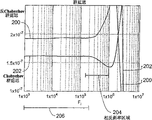
As mentioned above, the analog processing circuit of high expectations in mobile phone has filter and is included in wherein, and it can be provided at the rapid decay between passband and the stopband, and it can also show good group delay, and particularly do not show differential group delay, thereby avoided inter symbol interference.Fig. 3 has compared by the group delay of the anti-Chebychev filter of line 200 expression with by the group delay of the Chebychev filter of line 202 expressions, and it is plotted as the function of frequency.Cps has been included in Fig. 3, in 4 and 5 the ordinate, thus can easily more multiple figure.As can be seen, in the example that Fig. 3 provides, for surpassing 2 * 10
5The frequency of radian per second, anti-Chebychev group delay begin to increase.But for surpassing 2 * 10
5The angular frequency of radian per second, the Chebychev group delay begins to reduce, and this reducing continues up to frequency 10
6The radian per second, the Chebychev group delay sharply increases then.Should be appreciated that group delay therein is in the restricted area 204 of contrary sign, can obtain the partial offset to group delay frequency characteristic, thereby extended zone 206 effectively, this zone 206 extends to up to about 2 * 10 from low frequency
5The radian per second, wherein group delay with respect to frequency be basically constant up to increase 10
6Radian per second upper end frequency.
Fig. 4 schematically be used for the amplitude response of anti-Chebychev and Chebychev filter, its group delay is shown in Figure 3.As can be seen, anti-Chebychev filter in this example has smooth basically amplitude response up to about 10
6The radian per second, and amplitude response drops sharply to 5 * 10 then
6The trap that the radian per second occurs.At that point, response amplitude is suppressed above 60dB.The Chebychev filter also has basically amplitude response uniformly in passband, but has about 2 * 10
6The toggle frequency of radian per second descends rapidly from this frequency amplitude.
Fig. 5 shows the combined magnitude response of the anti-Chebychev filter of Chebychev/ of use independent filter as shown in Figure 3 and Figure 4.As can be seen, array response 210 is smooth basically, up to 10
6The radian per second, and sharply descend then, 2 * 10
6The 10dB that descends approximately of radian per second place, and 5 * 10
6Radian per second place descends and surpasses 60dB.And group delay can remain substantial constant up to rising to 1 * 10
6The radian per second.
It should be understood by one skilled in the art that Design of Analog Filter is extremely complex mathematical computing.But be known that a lot of designs analyze and describe it with normalized form, thereby the engineer can use " tricks of the trade " of canonical form effectively, to design specific filter characteristic.In addition, computer-aided design job contract tool also allows accurately to describe filter characteristic now.Owing to these reasons, the details of design does not need to describe in detail, because exist enough supports to make those of ordinary skills can realize this filter in the prior art.But for the specific filter of its response shown in Fig. 3 to 5, the utmost point position of anti-Chebychev response is calculated utmost point position by first of Chebychev response and is calculated, and uses the utmost point to replace.
Effectively the utmost point is present in negative half on S plane.
The position of stopband " zero ".
Employed anti-Chebychev transfer function is:
The polynomial utmost point position of separating of Chebychev is:
Effectively the utmost point is present in negative half on S plane.
Employed Chebychev transfer function is:
The transfer function of compound filter is the combination of two independent transfer functions:
x
i:=(Hc
i·Hic
i)
As compound filter, can be individually in two elements of filter each be adjusted into customized better filter response, to satisfy the demand of application-specific.
For example, for the Chebychev response, can adjust down every:
1. cut-off frequency
2. filter order (number of the utmost point)
3. ripple in being with
For anti-Chebychev filter, can adjust the following:
1. minimum stop-band attenuation
2. maximum permission passband roll-offs
3. reach the relative frequency of minimum stop-band attenuation
4. filter order
Can be by the stacked filter order (being that these levels are connected to one another) of adjusting that filter is embodied as filter stage, one or more thus levels can be switched out that this is stacked, so that they are by bypass.Therefore, level of bypass has just reduced the exponent number of filter.
Fig. 6 schematically shows the double-mode GSM/UMTS transceiver that constitutes one embodiment of the invention.This transceiver generally includes send channel 300 and receive channel 302.Although in Fig. 6, represent that with the form of simplifying in fact send channel 300 has comprised as dual-mode transmitter shown in Figure 1 in this paper accompanying drawing.In order to simplify understanding to Fig. 6, will be with identical reference marker among Fig. 6 with similar those parts of part shown in Figure 1, therefore as can be seen, transmitter receives the frequency synthesized signal from synthesizer 3, this composite signal before the homophase that is provided to upconverter and orthogonal mixer 15 and 17 through the frequency divider 9 of 3 frequency divisions.In the GSM pattern, the output of upconverter is provided to the phase-locked loop frequency shifter, and it comprises: phase detectors 21, voltage controlled oscillator 27, blender 25 and band pass filter 23.Therefore the description carried out as above-mentioned reference Fig. 1 of the operation of these assemblies.Can notice, the frequency divider 306,308 and 310 that in this transmitter architecture figure, also has 2 other frequency divisions, be to be understood that, these final operations for transmitter have very little entire effect, and particularly frequency divider 308 and 310 make effectively invalid each other, although the mark that their allow waveform and spacing and spacing are than being converted to desirable 50-50.Similarly, the UMTS path comprises linear amplifier array and upconverter.As shown in Figure 1 be labeled as 37,39,41 and 43 assembly schematically by 320 expressions of the frame among Fig. 6.
Should be appreciated that receiver section 302 is the reduced representation of Fig. 2.Here the multimode fractional expression multiplexer 124 of Fig. 2 is also specialized in two fractional expression synthesizers 3 shown in Figure 6.Can be clear that also two channels are provided, and each all has homophase and the orthogonal mixer that is used for received signal is down-converted to base band.The assembly 130,132,134,136,140,142,150,152,160 and 162 of Fig. 2 is schematically by 330 expressions of the frame among Fig. 6.Can be clear, two transmitter channel are shared these assemblies, and two receiver channels are shared these assemblies, and Receiver And Transmitter shared frequencies synthesizer assembly in fact.The embodiment that all provides its independent function with in these assemblies wherein each is compared, this assembly is shared the cost that can make aspect the final price of integrated circuit and is lowered, and also reduced the overall power consumption of transceiver, and therefore duplicate effectively.
GSM is operated in time division multiplex system, and therefore transmitter and receiver is not operated simultaneously.But UMTS operates on the full duplex, and therefore transmitter and receiver is to operate simultaneously.In the UMTS pattern, importantly restriction is owing to subtracting of the receiver that causes alternately with the UMTS transmitter is quick.This can obtain in the following manner: at first low noise amplifier and chip self is not integrated, and secondly by being limited in the transmitter power of transmitter output pin.And guarantee that importantly the noise level in emission output place frequency acceptance band is suitable.For example, by having the outside low noise amplifier of 13dB gain, transmitting power at transmitter output pin place is limited in+3dBm and on frequency acceptance band-the shot noise radix of 140dBc/Hz, if obtain the isolation of 30dB between transmitter and receiver, then transmitter is approximately 0.1dB in the influence of receiver sensitivity.
Structure shown in Figure 6 can be operated and is used for several modes, and the frequency planning that is used for this transceiver can be as follows:
GSM850/900 receiving mode-synthesizer frequency is 3 times of RF frequency.
GSM1800/1900 receiving mode-synthesizer frequency is 1.5 times of carrier frequency.
UMTS receiving mode-synthesizer frequency is 1.5 times of RF carrier frequency.
GSM850/900 emission mode-synthesizer frequency is 3 times of RF carrier frequency, and intermediate frequency is 1/2 of a RF carrier frequency.
GSM1800/1900 emission mode-synthesizer frequency is 1.5 times of RF carrier frequency, and intermediate frequency is 1/4 of a RF carrier frequency.
UMTS emission mode-synthesizer frequency is 1.5 times of RF carrier frequency, and intermediate frequency is 1/4 of a RF carrier frequency.
Fig. 7 schematically shows mixing feed forward and the reverse feeding AGC (automatic gain control) system that constitutes one embodiment of the invention.This circuit diagram shows variable gain amplifier, and its output is provided to the anti-Chebychev filter of mixed C hebychev/, and by 402 expressions, it is described in front prevailingly.The output of compound filter 402 is provided to the input of other variable gain amplifier, this amplifier schematically is represented as three independently controlled variable gain amplifiers 404,406 and 408 of electronics, and they are together as the variable gain between 0 and the 54dB that are provided in the dB stride.The output that final amplifier 408 is provided is as the output 410 from automatic gain controller.
The feed forward controller usually by 420 expressions, comprises received signal intensity indication (RSSI) record strip, and it has the input that is connected to compound filter 402 outputs.The RSSI record strip is used to estimate the signal strength signal intensity in compound filter output place.RSSI record strip 422 produces the voltage of synthetic power of the filter output place signal that substantial linear represent with dBm in proportion to as its output 424.This output signal was carried out filtering by low pass filter 426 before the analog input 428 that is provided to 6 bit analog-digital converters 430.In response to " begin conversion " signal signal digitalized with at input 428 places of analog-digital converter 430, and the output of conversion is provided to filter gain logic controller 432.This filter gain logic controller has two inputs, and one is provided to register 434, be used to control the gain of variable gain amplifier 400, and another input is provided to 6 bit down-conversion counters 440 with 6 bit words.Therefore, counter can be loaded with the output of filter gain logic controller 432.
Signal in the UMTS receiver is the composite signal of desired signal, noise and any residual interference signal.With appearing at this composite signal digitlization of compound filter 402 outputs place, have the numeric word of the every bit of characteristic " A " dB with generation, wherein A represents arbitrary number.This control word is used to set the gain of variable gain amplifier.Variable gain amplifier is designed to have the gain reduction characteristic of the every bit of " A " dB.Like this, increase 5AdB if enter the signal level of receiver, then the Digital Control word will also increase by 5.This will cause the gain of variable gain amplifier 404,406 and 408 to reduce quantity is the synthetic gain of 5AdB.Therefore, the signal level in 410 outputs place of variable gain controller keeps constant basically.Because up to the present described mode is used the feed forward technology, therefore there is not the bandwidth influence that may influence the reverse feeding system.Therefore, can set up the gain of automatic gain controller rapidly, for example when switching operation modes or channel.After having obtained the composite signal level rapidly and having set up initial gain, carry out further gain controlling by feedback arrangement.
Feedback controller, usually by 450 expressions, comprising: rectifier 452, it is connected to the output of amplifier 408, to reduce to represent the rectified signal of amplifier 408 output place signal powers.Signal from rectifier 452 had carried out low-pass filtering by filter 454 before the input that is provided to window comparator 456, as what those of ordinary skills recognized, this comparator 456 is its input signal and the height and the low threshold value that define window relatively, and generation expression signal is the output 458 that is lower than the window threshold value or is higher than the window threshold value.Signal 458 is provided to the counting direction control input (on/input down) of counter 440.As shown in Figure 7, also window comparator 456 is configured to provide expression when to its output be within the border of definition window, and this output is sent to AND door 460, this is provided to the clock signal of counter 440 as gating.Therefore, when output 410 is within by window comparator 456 defined power bands, suppresses counter 440 and receive its clock signal.Clock signal 462 is also carried out AND-operation with " starting feedback " signal that AND door 464 (whether 464 pairs of feedback control loops of this AND door are operated provides whole control) is located.The output of AND door 464 is provided to the input of AND door 460, and its output is connected to the clock pin of counter 440.The output of counter 440 is provided to gain decoder 470, and this decoder 470 is set the gain of amplifier 404,406 and 408.
In use, signal level detecter and window comparator are used to guarantee that composite signal level and amplifier output remain on narrow scope, for example+/-0.5dB.If the composite signal level is higher than the threshold value of window comparator, on then starting/following counter, and gain is adjusted in each clock cycle.By this way, the time constant of clock setting feedback control loop.If the composite signal level is lower than the window comparator threshold value, on then also starting/following counter, but at this moment counting is in the opposite direction.As a result, the action of feedback control loop always guarantees that the composite signal level is to be controlled securely and to be adjusted by the determined speed of clock 462 frequencies.
With reference to figure 2, should be noted that when carrying out the gain controlling adjustment at every turn or carrying out offset correction that this stride adjustment can cause appearing at the transition DC skew of filter output.Can remove this DC skew by high pass filter, but for certain common receiver, the DC offset correction should be carried out at numeric field better.Therefore,, estimate new DC skew, and should estimate that the result was provided to transducer 134 and 136, make and add correction to adder 130 and 132 in each gain change place.In other words, the transition that occurs as gain change result still has unwanted influence for low pass filter 140 and 150.This transition declines in time, but during filter stabilization time, homodyne receiver is covered effectively.This is because be necessary to limit the conversion range of analog-digital converter, and skew can cause that transducer carries out the conversion outside its normal operation range.
Suppose that receiver is quit work between this transient period effectively, then the inventor has recognized that, so just allows to change filter characteristic in the short time period, to allow stabilization time faster.Therefore, when the change implemented gain or skew, high pass filter is simultaneously or near side by side being set to wide bandwidth, thereby fast and stable is got off in the DC transition.Can estimate this stabilization time from known filter characteristic.After stabilization time, filter automaticallyes switch and gets back to the required setting of nominal of its proper operation.Filter is controlled by timer, for example can be embodied as monostablely, and it changes filter characteristic in the time period of brief but good definition.This technique guarantee the fastest possible receiver stabilization time, and make the required adjustment amount of energy minimum that may remove by high pass filter simultaneously.Typical case's ratio between two kinds of bandwidth settings is about 10 to 1, although this only is a limiting examples, and also can be by other ratios of design alternative.The realization of this technology is not to depend on wave filter technology.Therefore filter can be implemented as switching capacity filter, switches bandwidth active R-C filter, circulator-capacitive filter or the like.The specific implementation of filter is in those of ordinary skills' ken.
Therefore a kind of multimode rake receiver and transceiver that is specially adapted in the mobile phone be provided.
Claims (14)
1. direct changing multi receiver, comprise the reconfigurable filter of at least one electronics, wherein this receiver can be operated in GSM and UMTS receiving mode to receive emission, wherein receive the signal of wanting filtering that obtains from the emission of above-mentioned reception by the reconfigurable filter of the described electronics that is combined to form of Chebychev filter and anti-Chebychev filter, and utilize the described Chebychev filter of series connection and the combination of described anti-Chebychev filter that resulting signal is carried out filtering, described filtering is included in the cut-off frequency zone, the first derivative of the group delay of the contrary sign that has of combination Chebychev filter and anti-Chebychev filter, in regional basic neutralisation group delay near cut-off frequency, and wherein adjust the operation of reconfigurable filter according to receiving mode, so that resulting signal is carried out filtering, and provide corresponding filtering signal to be used for further handling at described receiver.
2. receiver as claimed in claim 1, wherein the reconfigurable filter of electronics is a low pass filter.
3. receiver as claimed in claim 1, wherein the reconfigurable filter response of this at least one electronics is in the filter gain logic controller.
4. receiver as claimed in claim 1, wherein anti-Chebychev filter is controlled, thus adjust from comprise minimum stop-band attenuation, maximum allow frequency that passband roll-offs, reaches minimum stop-band attenuation, and the tabulation that constitutes of filter order select its at least one characteristic.
5. as each described receiver in the claim 1 to 4, wherein the Chebychev filter is controlled, with at least one characteristic in the tabulation of adjusting self-contained cut-off frequency, filter order and passband ripple formation.
6. receiver as claimed in claim 1, wherein receiver further comprises at least one DC skew generator in response to the filter gain logic controller, the reconfigurable filter response of described electronics is in the filter gain logic controller, in receiver, this DC skew is added into down-conversion signal, be offset thereby reduce the DC that appears in the receiver.
7. receiver as claimed in claim 1, wherein receiver has " homophase " channel and " quadrature " channel.
8. receiver as claimed in claim 1, further comprise variable gain amplifier in response to the filter gain logic controller, remaining in the signal amplitude of this variable gain amplifier output place in the preset range, the reconfigurable filter response of described electronics is in the filter gain logic controller.
9. receiver as claimed in claim 6, wherein the signal from receiver is converted into digital form by analog-digital converter, and control circuit is in response to this digital form, and uses it to draw will to be offset the DC skew that generator imposes on down-conversion signal by DC.
10. receiver as claimed in claim 6, further comprise first and second radio-frequency front-ends, described first or second radio-frequency front-end is used for being received at least one emission of first and second frequency bands, or is used for being received at least one emission of first and second emission modes.
11. receiver as claimed in claim 10, wherein first radio-frequency front-end is arranged to receive at least one in GSM850MHz and the GSM900MHz emission.
12. receiver as claimed in claim 10, at least one during wherein second radio-frequency front-end is arranged to receive in GSM1800MHz and the GSM1900MHz emission.
13. receiver as claimed in claim 10, wherein one of front end is arranged to receive at least one in UMTS2100MHz and the UMTS1900MHz emission.
14. receiver as claimed in claim 1, wherein the group delay of the group delay of Chebychev filter and anti-Chebychev filter cancels each other out in the zone near the cut-off frequency of filter basically.
Applications Claiming Priority (5)
| Application Number | Priority Date | Filing Date | Title |
|---|---|---|---|
| GBGB0204108.5A GB0204108D0 (en) | 2002-02-21 | 2002-02-21 | 3G radio |
| GB0204108.5 | 2002-02-21 | ||
| US10/331,622 US7292649B2 (en) | 2002-02-21 | 2002-12-30 | 3G radio |
| US10/331,622 | 2002-12-30 | ||
| PCT/US2003/005473 WO2003073631A1 (en) | 2002-02-21 | 2003-02-21 | 3g radio |
Publications (2)
| Publication Number | Publication Date |
|---|---|
| CN1639990A CN1639990A (en) | 2005-07-13 |
| CN1639990B true CN1639990B (en) | 2010-09-15 |
Family
ID=27767096
Family Applications (1)
| Application Number | Title | Priority Date | Filing Date |
|---|---|---|---|
| CN03804376.9A Expired - Lifetime CN1639990B (en) | 2002-02-21 | 2003-02-21 | Direct conversion multi-mode receiver |
Country Status (4)
| Country | Link |
|---|---|
| EP (1) | EP1476950B1 (en) |
| JP (1) | JP4338526B2 (en) |
| CN (1) | CN1639990B (en) |
| WO (1) | WO2003073631A1 (en) |
Families Citing this family (8)
| Publication number | Priority date | Publication date | Assignee | Title |
|---|---|---|---|---|
| GB0204108D0 (en) | 2002-02-21 | 2002-04-10 | Analog Devices Inc | 3G radio |
| US7231193B2 (en) * | 2004-04-13 | 2007-06-12 | Skyworks Solutions, Inc. | Direct current offset correction systems and methods |
| US7379752B2 (en) * | 2004-10-13 | 2008-05-27 | Mediatek Inc. | Methods and apparatus for communication in a wireless system |
| JP5274014B2 (en) | 2004-10-13 | 2013-08-28 | メディアテック インコーポレーテッド | Communication system filter |
| JP5202035B2 (en) * | 2008-02-28 | 2013-06-05 | ルネサスエレクトロニクス株式会社 | Semiconductor integrated circuit and operation method thereof |
| EP2259520A1 (en) * | 2009-06-02 | 2010-12-08 | ST-Ericsson SA | Process for computing a frequency offset for a UMTS communication system based on the CPICH pilot signals |
| JP5500203B2 (en) * | 2012-05-18 | 2014-05-21 | 住友電気工業株式会社 | Soft decision decoding apparatus and soft decision decoding program |
| US9543997B2 (en) * | 2014-01-21 | 2017-01-10 | Infineon Technologies Ag | System and method for a mixer |
Citations (7)
| Publication number | Priority date | Publication date | Assignee | Title |
|---|---|---|---|---|
| US5719326A (en) * | 1996-10-25 | 1998-02-17 | Harris Corporation | Reconfigurable filter system |
| US5896562A (en) * | 1996-04-01 | 1999-04-20 | Nokia Mobile Phones, Ltd. | Transmitter/receiver for transmitting and receiving of an RF signal in two frequency bands |
| US6043727A (en) * | 1998-05-15 | 2000-03-28 | Hughes Electronics Corporation | Reconfigurable millimeterwave filter using stubs and stub extensions selectively coupled using voltage actuated micro-electro-mechanical switches |
| US6130590A (en) * | 1998-08-14 | 2000-10-10 | Lucent Technologies Inc. | Programmable filter bank having notch filter and bandpass filter frequency responses |
| US6185434B1 (en) * | 1996-09-11 | 2001-02-06 | Lk-Products Oy | Antenna filtering arrangement for a dual mode radio communication device |
| US6215988B1 (en) * | 1997-05-15 | 2001-04-10 | Nokia Mobile Phones, Ltd. | Dual band architectures for mobile stations |
| WO2002013473A1 (en) * | 2000-08-04 | 2002-02-14 | Motorola Inc. | Apparatus for reducing dc offset in a receiver |
Family Cites Families (2)
| Publication number | Priority date | Publication date | Assignee | Title |
|---|---|---|---|---|
| FI950106A (en) * | 1995-01-10 | 1996-07-11 | Nokia Mobile Phones Ltd | Procedure and coupling for filtering interference in radio receiver receivers |
| FI112741B (en) * | 1998-11-26 | 2003-12-31 | Nokia Corp | Method and arrangement for transmitting and receiving RF signals at various radio interfaces of communication systems |
-
2003
- 2003-02-21 JP JP2003572192A patent/JP4338526B2/en not_active Expired - Lifetime
- 2003-02-21 CN CN03804376.9A patent/CN1639990B/en not_active Expired - Lifetime
- 2003-02-21 WO PCT/US2003/005473 patent/WO2003073631A1/en active Application Filing
- 2003-02-21 EP EP03709295A patent/EP1476950B1/en not_active Expired - Lifetime
Patent Citations (7)
| Publication number | Priority date | Publication date | Assignee | Title |
|---|---|---|---|---|
| US5896562A (en) * | 1996-04-01 | 1999-04-20 | Nokia Mobile Phones, Ltd. | Transmitter/receiver for transmitting and receiving of an RF signal in two frequency bands |
| US6185434B1 (en) * | 1996-09-11 | 2001-02-06 | Lk-Products Oy | Antenna filtering arrangement for a dual mode radio communication device |
| US5719326A (en) * | 1996-10-25 | 1998-02-17 | Harris Corporation | Reconfigurable filter system |
| US6215988B1 (en) * | 1997-05-15 | 2001-04-10 | Nokia Mobile Phones, Ltd. | Dual band architectures for mobile stations |
| US6043727A (en) * | 1998-05-15 | 2000-03-28 | Hughes Electronics Corporation | Reconfigurable millimeterwave filter using stubs and stub extensions selectively coupled using voltage actuated micro-electro-mechanical switches |
| US6130590A (en) * | 1998-08-14 | 2000-10-10 | Lucent Technologies Inc. | Programmable filter bank having notch filter and bandpass filter frequency responses |
| WO2002013473A1 (en) * | 2000-08-04 | 2002-02-14 | Motorola Inc. | Apparatus for reducing dc offset in a receiver |
Non-Patent Citations (2)
| Title |
|---|
| 程佩青.数字信号处理教程 2.清华大学出版社,1995,110-111,142-153. |
| 程佩青.数字信号处理教程 2.清华大学出版社,1995,110-111,142-153. * |
Also Published As
| Publication number | Publication date |
|---|---|
| EP1476950B1 (en) | 2008-08-13 |
| EP1476950A4 (en) | 2005-07-20 |
| CN1639990A (en) | 2005-07-13 |
| JP2005518750A (en) | 2005-06-23 |
| EP1476950A1 (en) | 2004-11-17 |
| WO2003073631A1 (en) | 2003-09-04 |
| JP4338526B2 (en) | 2009-10-07 |
Similar Documents
| Publication | Publication Date | Title |
|---|---|---|
| US7106805B2 (en) | 3G radio | |
| US6125266A (en) | Dual band architectures for mobile stations having transmitter linearization feedback | |
| US7092676B2 (en) | Shared functional block multi-mode multi-band communication transceivers | |
| US8838049B1 (en) | Method and arrangement for transmitting and receiving RF signals through various radio interfaces of communication systems | |
| US20160043822A1 (en) | Radio frequency receiver and receiving method | |
| GB2310342A (en) | Dual mode radio transceiver front end | |
| CN102664653A (en) | Mobile terminal and radio frequency front terminal thereof with radio frequency digital-to-analog conversion type linear transmitter | |
| CN101273533B (en) | EDGE transceiver architecture and related methods | |
| CN1639990B (en) | Direct conversion multi-mode receiver | |
| JP3672189B2 (en) | Radio signal receiving apparatus and demodulation processing circuit | |
| KR101053136B1 (en) | Shared function block multimode multiband communication transceiver | |
| CN1640085A (en) | 3G radio device | |
| JP3309904B2 (en) | Wireless transceiver | |
| US6647247B2 (en) | Method for producing transmission frequency | |
| GB2332109A (en) | A tunable voltage controlled bandpass filter for a direct conversion receiver | |
| JPH1093475A (en) | Composite system shared terminal equipment | |
| CN102723964A (en) | Radio frequency front-end transceiver of silent surface filter of multi-standard mobile terminal | |
| JP2007081708A (en) | Wireless device | |
| WO2003073659A2 (en) | 3g radio | |
| WO2003073660A2 (en) | 3g radio | |
| WO2003073636A1 (en) | 3g radio | |
| KR20010059817A (en) | Advanced time division duplexing(tdd) type rf signal tx/rx apparatus |
Legal Events
| Date | Code | Title | Description |
|---|---|---|---|
| C06 | Publication | ||
| PB01 | Publication | ||
| C10 | Entry into substantive examination | ||
| SE01 | Entry into force of request for substantive examination | ||
| ASS | Succession or assignment of patent right |
Owner name: MEDIATEK INC. Free format text: FORMER OWNER: ANALOG DEVICES INC. Effective date: 20080404 |
|
| C41 | Transfer of patent application or patent right or utility model | ||
| TA01 | Transfer of patent application right |
Effective date of registration: 20080404 Address after: Hsinchu Science Industrial Park, Taiwan Applicant after: MEDIATEK Inc. Address before: Massachusetts, USA Applicant before: ANALOG DEVICES, Inc. |
|
| C14 | Grant of patent or utility model | ||
| GR01 | Patent grant | ||
| CX01 | Expiry of patent term |
Granted publication date: 20100915 |
|
| CX01 | Expiry of patent term |