CN1577832A - Semiconductor device and method for fabricating the same - Google Patents
Semiconductor device and method for fabricating the same Download PDFInfo
- Publication number
- CN1577832A CN1577832A CNA2004100621554A CN200410062155A CN1577832A CN 1577832 A CN1577832 A CN 1577832A CN A2004100621554 A CNA2004100621554 A CN A2004100621554A CN 200410062155 A CN200410062155 A CN 200410062155A CN 1577832 A CN1577832 A CN 1577832A
- Authority
- CN
- China
- Prior art keywords
- dielectric film
- wiring
- fuse
- contrary
- metal
- Prior art date
- Legal status (The legal status is an assumption and is not a legal conclusion. Google has not performed a legal analysis and makes no representation as to the accuracy of the status listed.)
- Pending
Links
- 239000004065 semiconductor Substances 0.000 title claims abstract description 129
- 238000000034 method Methods 0.000 title claims description 85
- 229910052751 metal Inorganic materials 0.000 claims abstract description 144
- 239000002184 metal Substances 0.000 claims abstract description 144
- 239000000758 substrate Substances 0.000 claims abstract description 25
- 238000009792 diffusion process Methods 0.000 claims abstract description 24
- 238000004519 manufacturing process Methods 0.000 claims description 97
- 230000015572 biosynthetic process Effects 0.000 claims description 55
- 238000005530 etching Methods 0.000 claims description 29
- 230000004888 barrier function Effects 0.000 abstract description 137
- RYGMFSIKBFXOCR-UHFFFAOYSA-N Copper Chemical compound [Cu] RYGMFSIKBFXOCR-UHFFFAOYSA-N 0.000 description 83
- 229910052802 copper Inorganic materials 0.000 description 83
- 239000010949 copper Substances 0.000 description 83
- 230000015556 catabolic process Effects 0.000 description 31
- 238000009413 insulation Methods 0.000 description 31
- 238000005516 engineering process Methods 0.000 description 28
- 239000000047 product Substances 0.000 description 21
- 230000000694 effects Effects 0.000 description 18
- 239000000463 material Substances 0.000 description 14
- 229910010271 silicon carbide Inorganic materials 0.000 description 14
- 239000007769 metal material Substances 0.000 description 12
- 229910052581 Si3N4 Inorganic materials 0.000 description 7
- PCHJSUWPFVWCPO-UHFFFAOYSA-N gold Chemical compound [Au] PCHJSUWPFVWCPO-UHFFFAOYSA-N 0.000 description 7
- 229910052737 gold Inorganic materials 0.000 description 7
- 239000010931 gold Substances 0.000 description 7
- 229910000510 noble metal Inorganic materials 0.000 description 7
- HQVNEWCFYHHQES-UHFFFAOYSA-N silicon nitride Chemical compound N12[Si]34N5[Si]62N3[Si]51N64 HQVNEWCFYHHQES-UHFFFAOYSA-N 0.000 description 7
- 229910052709 silver Inorganic materials 0.000 description 7
- 239000004332 silver Substances 0.000 description 7
- 238000009713 electroplating Methods 0.000 description 5
- 238000004544 sputter deposition Methods 0.000 description 5
- 238000000059 patterning Methods 0.000 description 4
- 230000003628 erosive effect Effects 0.000 description 3
- 239000004411 aluminium Substances 0.000 description 2
- 229910052782 aluminium Inorganic materials 0.000 description 2
- XAGFODPZIPBFFR-UHFFFAOYSA-N aluminium Chemical compound [Al] XAGFODPZIPBFFR-UHFFFAOYSA-N 0.000 description 2
- 238000010276 construction Methods 0.000 description 2
- 238000000151 deposition Methods 0.000 description 2
- 230000008021 deposition Effects 0.000 description 2
- RTAQQCXQSZGOHL-UHFFFAOYSA-N Titanium Chemical compound [Ti] RTAQQCXQSZGOHL-UHFFFAOYSA-N 0.000 description 1
- NRTOMJZYCJJWKI-UHFFFAOYSA-N Titanium nitride Chemical compound [Ti]#N NRTOMJZYCJJWKI-UHFFFAOYSA-N 0.000 description 1
- 229910021417 amorphous silicon Inorganic materials 0.000 description 1
- 230000007423 decrease Effects 0.000 description 1
- 239000012467 final product Substances 0.000 description 1
- 238000003475 lamination Methods 0.000 description 1
- 239000002245 particle Substances 0.000 description 1
- 238000003892 spreading Methods 0.000 description 1
- 239000010936 titanium Substances 0.000 description 1
- 229910052719 titanium Inorganic materials 0.000 description 1
- 239000011800 void material Substances 0.000 description 1
Images


Classifications
-
- H—ELECTRICITY
- H01—ELECTRIC ELEMENTS
- H01L—SEMICONDUCTOR DEVICES NOT COVERED BY CLASS H10
- H01L21/00—Processes or apparatus adapted for the manufacture or treatment of semiconductor or solid state devices or of parts thereof
- H01L21/70—Manufacture or treatment of devices consisting of a plurality of solid state components formed in or on a common substrate or of parts thereof; Manufacture of integrated circuit devices or of parts thereof
- H01L21/71—Manufacture of specific parts of devices defined in group H01L21/70
- H01L21/768—Applying interconnections to be used for carrying current between separate components within a device comprising conductors and dielectrics
- H01L21/76801—Applying interconnections to be used for carrying current between separate components within a device comprising conductors and dielectrics characterised by the formation and the after-treatment of the dielectrics, e.g. smoothing
- H01L21/76802—Applying interconnections to be used for carrying current between separate components within a device comprising conductors and dielectrics characterised by the formation and the after-treatment of the dielectrics, e.g. smoothing by forming openings in dielectrics
- H01L21/76807—Applying interconnections to be used for carrying current between separate components within a device comprising conductors and dielectrics characterised by the formation and the after-treatment of the dielectrics, e.g. smoothing by forming openings in dielectrics for dual damascene structures
- H01L21/76808—Applying interconnections to be used for carrying current between separate components within a device comprising conductors and dielectrics characterised by the formation and the after-treatment of the dielectrics, e.g. smoothing by forming openings in dielectrics for dual damascene structures involving intermediate temporary filling with material
-
- H—ELECTRICITY
- H01—ELECTRIC ELEMENTS
- H01L—SEMICONDUCTOR DEVICES NOT COVERED BY CLASS H10
- H01L21/00—Processes or apparatus adapted for the manufacture or treatment of semiconductor or solid state devices or of parts thereof
- H01L21/70—Manufacture or treatment of devices consisting of a plurality of solid state components formed in or on a common substrate or of parts thereof; Manufacture of integrated circuit devices or of parts thereof
- H01L21/71—Manufacture of specific parts of devices defined in group H01L21/70
- H01L21/768—Applying interconnections to be used for carrying current between separate components within a device comprising conductors and dielectrics
- H01L21/76801—Applying interconnections to be used for carrying current between separate components within a device comprising conductors and dielectrics characterised by the formation and the after-treatment of the dielectrics, e.g. smoothing
- H01L21/76802—Applying interconnections to be used for carrying current between separate components within a device comprising conductors and dielectrics characterised by the formation and the after-treatment of the dielectrics, e.g. smoothing by forming openings in dielectrics
- H01L21/76807—Applying interconnections to be used for carrying current between separate components within a device comprising conductors and dielectrics characterised by the formation and the after-treatment of the dielectrics, e.g. smoothing by forming openings in dielectrics for dual damascene structures
-
- H—ELECTRICITY
- H01—ELECTRIC ELEMENTS
- H01L—SEMICONDUCTOR DEVICES NOT COVERED BY CLASS H10
- H01L23/00—Details of semiconductor or other solid state devices
- H01L23/52—Arrangements for conducting electric current within the device in operation from one component to another, i.e. interconnections, e.g. wires, lead frames
- H01L23/522—Arrangements for conducting electric current within the device in operation from one component to another, i.e. interconnections, e.g. wires, lead frames including external interconnections consisting of a multilayer structure of conductive and insulating layers inseparably formed on the semiconductor body
- H01L23/525—Arrangements for conducting electric current within the device in operation from one component to another, i.e. interconnections, e.g. wires, lead frames including external interconnections consisting of a multilayer structure of conductive and insulating layers inseparably formed on the semiconductor body with adaptable interconnections
- H01L23/5252—Arrangements for conducting electric current within the device in operation from one component to another, i.e. interconnections, e.g. wires, lead frames including external interconnections consisting of a multilayer structure of conductive and insulating layers inseparably formed on the semiconductor body with adaptable interconnections comprising anti-fuses, i.e. connections having their state changed from non-conductive to conductive
-
- H—ELECTRICITY
- H01—ELECTRIC ELEMENTS
- H01L—SEMICONDUCTOR DEVICES NOT COVERED BY CLASS H10
- H01L23/00—Details of semiconductor or other solid state devices
- H01L23/52—Arrangements for conducting electric current within the device in operation from one component to another, i.e. interconnections, e.g. wires, lead frames
- H01L23/522—Arrangements for conducting electric current within the device in operation from one component to another, i.e. interconnections, e.g. wires, lead frames including external interconnections consisting of a multilayer structure of conductive and insulating layers inseparably formed on the semiconductor body
- H01L23/532—Arrangements for conducting electric current within the device in operation from one component to another, i.e. interconnections, e.g. wires, lead frames including external interconnections consisting of a multilayer structure of conductive and insulating layers inseparably formed on the semiconductor body characterised by the materials
- H01L23/5329—Insulating materials
- H01L23/53295—Stacked insulating layers
-
- H—ELECTRICITY
- H01—ELECTRIC ELEMENTS
- H01L—SEMICONDUCTOR DEVICES NOT COVERED BY CLASS H10
- H01L27/00—Devices consisting of a plurality of semiconductor or other solid-state components formed in or on a common substrate
- H01L27/02—Devices consisting of a plurality of semiconductor or other solid-state components formed in or on a common substrate including semiconductor components specially adapted for rectifying, oscillating, amplifying or switching and having potential barriers; including integrated passive circuit elements having potential barriers
- H01L27/04—Devices consisting of a plurality of semiconductor or other solid-state components formed in or on a common substrate including semiconductor components specially adapted for rectifying, oscillating, amplifying or switching and having potential barriers; including integrated passive circuit elements having potential barriers the substrate being a semiconductor body
- H01L27/10—Devices consisting of a plurality of semiconductor or other solid-state components formed in or on a common substrate including semiconductor components specially adapted for rectifying, oscillating, amplifying or switching and having potential barriers; including integrated passive circuit elements having potential barriers the substrate being a semiconductor body including a plurality of individual components in a repetitive configuration
- H01L27/118—Masterslice integrated circuits
- H01L27/11803—Masterslice integrated circuits using field effect technology
-
- H—ELECTRICITY
- H01—ELECTRIC ELEMENTS
- H01L—SEMICONDUCTOR DEVICES NOT COVERED BY CLASS H10
- H01L2924/00—Indexing scheme for arrangements or methods for connecting or disconnecting semiconductor or solid-state bodies as covered by H01L24/00
- H01L2924/0001—Technical content checked by a classifier
- H01L2924/0002—Not covered by any one of groups H01L24/00, H01L24/00 and H01L2224/00
Landscapes
- Engineering & Computer Science (AREA)
- Physics & Mathematics (AREA)
- Condensed Matter Physics & Semiconductors (AREA)
- General Physics & Mathematics (AREA)
- Computer Hardware Design (AREA)
- Microelectronics & Electronic Packaging (AREA)
- Power Engineering (AREA)
- Manufacturing & Machinery (AREA)
- Design And Manufacture Of Integrated Circuits (AREA)
- Internal Circuitry In Semiconductor Integrated Circuit Devices (AREA)
Abstract
A semiconductor device has a first metal pattern made of a first metal formed on a semiconductor substrate, an insulating film formed over the first metal pattern, and a second metal pattern made of a second metal formed on the insulating film. The insulating film has a barrier property for preventing the diffusion of the first metal.
Description
Technical field
The present invention relates to a kind of semiconductor device and manufacture method thereof, particularly get final product used contrary fuse (anti-fuse) structure and manufacture method thereof in the reconstituted logic element at FPGA (FieldProgrammable Gate Array) element.
Background technology
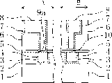
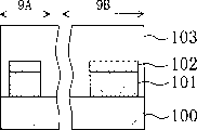
Below, with reference to figure 9 (a)~Fig. 9 (f), the manufacture method of the semiconductor device relevant with background technology is described, particularly, be the manufacture method of contrary fuse.
Fig. 9 (a)~Fig. 9 (f) is the profile of the master operation in the manufacture method of the related semiconductor device of display background technology.
At first, shown in Fig. 9 (a), the wiring layer 101a that deposition is made by metal materials such as aluminium on Semiconductor substrate 100.Need mention, to can be the upper and lower of aluminium lamination be the laminated construction of the metal material of representative with titanium or titanium nitride etc. to wiring layer 101a here.Then, first dielectric film 102 that deposition is made by amorphous silicon etc. on wiring layer 101a with contrary fuse function.
Then, shown in Fig. 9 (b), wiring layer 101a and first dielectric film, 102 patternings are formed wiring 101 by photo-mask process and etching work procedure.
Then, shown in Fig. 9 (c), on Semiconductor substrate 100, form second dielectric film 103 and with wiring layer 101a be patterned formed wiring 101 and patterning first dielectric film 102 cover.
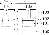
Then, shown in Fig. 9 (d), etching second dielectric film 103 and form first through hole (via hole), 104 and second through hole 105 lead to above the first dielectric film film 102.Need mention, first dielectric film 102 with contrary fuse function exposes from the bottom of first through hole 104 and second through hole 105.
Then, shown in Fig. 9 (e), form etchant resist 106 so that only will be formed on second through hole, 105 coverings that contrary fuse forms regional 9B.Then, serve as that shielding is removed the part that is present in first through hole, 104 bottoms in first dielectric film 102 by etching with corrosion-resisting pattern 106 again, couple together so that be formed on first through hole 104 and the wiring 101 that circuit forms regional 9A.Afterwards, remove etchant resist 106 again.
Then, shown in Fig. 9 (f), utilize CVD and CMP technology etc. to fill first through hole 104 and second through hole 105 and form first stopple (via plug), 107 and second stopple 108 with metal material.
As mentioned above, contrary fuse 109 is formed on contrary fuse and forms among the regional 9B and (for example refer to Patent Document 1).
The publication communique spy of [patent documentation 1] Japan opens flat 6-97171 communique
Yet, in the manufacture method of the related semiconductor device of background technology, need in the zone beyond contrary fuse forms regional 9B, in other words, circuit forms among the regional 9A, forms the operation of first dielectric film 102 with contrary fuse function at least.So, with form the operation that does not adopt among the regional 9A under contrary that situation of fuse-wires structure at contrary fuse and compare, that is compare in the operation that contrary fuse forms under that a kind of situation that does not form first dielectric film 102 with contrary fuse function among the regional 9A, operation road number has increased, so manufacturing cost increases; Because along with the increase of process number, particle also increases, so probably product percent of pass can descend; Compare with the sort of situation of 101 patternings that only will connect up, forming among the regional 9A circuit by first dielectric film 102 with contrary fuse function and the wiring 101 laminated construction patternings that constitute is the very things of difficulty; And, shown in Fig. 9 (f), probably form first dielectric film 102 that has contrary fuse function among the regional 9B and circuit and form between the wiring 101 among the regional 9A and can imbed bad and space (void) 103a occurs because of second dielectric film 103 at contrary fuse.
Summary of the invention
Developmental research comes out in order to address the above problem just in the present invention, and its purpose is: provide a kind of operation road number to reduce, and realized the semiconductor device and the manufacture method thereof of manufacturing cost decline, product percent of pass raising etc.
For achieving the above object, first kind of semiconductor device involved in the present invention, comprise: be formed on the Semiconductor substrate by first metal first metal pattern, be formed on the dielectric film on first metal pattern, and be formed on the dielectric film by second metal second metal pattern; Dielectric film has for preventing the block of described first metal diffusing.
According to first semiconductor device, can realize to utilize damascene to connect up and form for example contrary fuse-wires structure of copper wiring formation operation manufacturing of the such common wiring formation operation of operation.Therefore, can realize the contrary fuse-wires structure that to make with the process number that the road number that forms operation than existing contrary fuse also lack.The result is to access the semiconductor device that production cost descends, product percent of pass improves.
In first semiconductor device involved in the present invention, preferably contain first metal that diffusion comes in the dielectric film.
So, because contain first metal that diffusion comes in the dielectric film, so dielectric film plays can easily take place owing to applying voltage the contrary fuse of insulation breakdown.
In first semiconductor device involved in the present invention, preferably second metal pattern forms the appearance that sinks in the described dielectric film.
So, because second metal pattern forms the appearance that sinks in the described dielectric film, so dielectric film plays can easily take place owing to applying voltage the contrary fuse of insulation breakdown.
In first semiconductor device involved in the present invention, preferably first metal pattern is wiring or stopple.
So, can realize to utilize the damascene wiring to form the contrary fuse-wires structure that operation is made.
In first semiconductor device involved in the present invention, preferably second metal pattern is wiring or stopple.
So, can realize to utilize the damascene wiring to form the contrary fuse-wires structure that operation is made.And, be under the situation of stopple at second metal pattern, can reduce forming the contrary required area of fuse.
Second semiconductor device involved in the present invention comprises: be formed on the Semiconductor substrate by first metal first metal pattern, be formed on the dielectric film on first metal pattern, and be formed on the dielectric film by second metal second metal pattern.Dielectric film has for preventing the block of described first metal diffusing.Second metal pattern forms: form the regional break-through dielectric film and the first metal pattern conducting at circuit, simultaneously form the zone at contrary fuse and make dielectric film between between it and first metal pattern.
According to second semiconductor device, can realize to utilize damascene to connect up and form for example contrary fuse-wires structure of copper wiring formation operation manufacturing of the such common wiring formation operation of operation.Therefore, can realize the contrary fuse-wires structure that to make with the process number that the road number that forms operation than existing contrary fuse also lack.The result is to access the semiconductor device that production cost descends, product percent of pass improves.
In second semiconductor device involved in the present invention, preferably contain first metal that diffusion comes in the dielectric film.
So, because contain first metal that diffusion comes in the dielectric film, so dielectric film plays can easily take place owing to applying voltage the contrary fuse of insulation breakdown.
In second semiconductor device involved in the present invention, preferably second metal pattern forms the appearance that sinks in the described dielectric film.
So, because second metal pattern forms the appearance that sinks in the dielectric film, so dielectric film plays can easily take place owing to applying voltage the contrary fuse of insulation breakdown.
In second semiconductor device involved in the present invention, preferably first metal pattern is wiring or stopple.
So, can realize to utilize the damascene wiring to form the contrary fuse-wires structure that operation is made.
In second semiconductor device involved in the present invention, preferably second metal pattern is wiring or stopple.
So, can realize to utilize the damascene wiring to form the contrary fuse-wires structure that operation is made.And, be under the situation of stopple at second metal pattern, can reduce forming the contrary required area of fuse.
The manufacture method of first semiconductor device involved in the present invention, comprise: on Semiconductor substrate, form step by the first metal wiring, in wiring, form the step of first dielectric film, on first dielectric film, form the step of second dielectric film, circuit form zone and contrary fuse form form respectively on second dielectric film in the zone be positioned at wiring above allow the step of the opening portion that first dielectric film exposes simultaneously, forming corrosion-resisting pattern forms after the opening portion in zone to cover contrary fuse, do shielding with this corrosion-resisting pattern again and carry out etching, first dielectric film that the bottom of opening portion that forms the zone from circuit is exposed is removed and the step that allows wiring expose, and remove after the corrosion-resisting pattern, form that the opening portion in zone and opening portion that contrary fuse forms the zone are imbedded second metal respectively and the step that forms metal pattern at circuit; First dielectric film has the block that prevents first metal diffusing.
Manufacture method according to first semiconductor device, by shielding and carry out etching against the opening portion that fuse forms the zone, and the limit forms regional formation and the metal pattern that connects up conducting at circuit, and the limit can form the regional structure that first dielectric film becomes contrary fuse that forms at contrary fuse.So, can realize utilizing damascene to connect up and form for example contrary fuse-wires structure of copper wiring formation operation manufacturing of the such common wiring formation operation of operation.Therefore, can realize the contrary fuse-wires structure that to make with the process number that the road number that forms operation than existing contrary fuse also lack.The result is, the manufacture method of the semiconductor device that can provide that a kind of production cost descends, product percent of pass has improved.
The manufacture method of second semiconductor device involved in the present invention, comprise: on Semiconductor substrate, form step by the first metal wiring, in wiring, form the step of first dielectric film, on first dielectric film, form the step of second dielectric film, circuit form zone and contrary fuse form form respectively on second dielectric film in the zone be positioned at wiring above allow the step of first opening portion that first dielectric film exposes simultaneously, forming when the photoresistance pattern that is formed by the eurymeric photoresistance of second opening portion is formed at the top that contrary fuse forms first opening portion in zone, so that the nubbin of the eurymeric photoresistance that forms serves as to shield to carry out etching by exposing inadequately, form the step that first dielectric film that exposes from the bottom of first opening portion in the zone allows wiring expose and remove circuit, and remove after the corrosion-resisting pattern, form that first opening portion in zone and first opening portion that contrary fuse forms the zone are imbedded second metal respectively and the step that forms metal pattern at circuit; First dielectric film has the block that prevents first metal diffusing.
Manufacture method according to second semiconductor device, when having hidden contrary fuse and having formed first opening portion in the zone, carry out etching to utilize the not enough and nubbin work eurymeric photoresistance that forms of exposure when forming the photoresistance pattern that forms by the eurymeric photoresistance of second opening portion to shield, and the limit forms the zone at circuit and forms metal pattern with the wiring conducting, and the limit can be formed in contrary fuse and forms the structure that regional first dielectric film becomes contrary fuse.So, can realize utilizing damascene to connect up and form for example contrary fuse-wires structure of copper wiring formation operation manufacturing of the such common wiring formation operation of operation.Therefore, can realize the contrary fuse-wires structure that to make with the process number that the road number that forms operation than existing contrary fuse also lack.The result is, the manufacture method of the semiconductor device that can provide that a kind of production cost descends, product percent of pass has improved.
The manufacture method of the 3rd semiconductor device involved in the present invention, comprise: on Semiconductor substrate, form step by the first metal wiring, in wiring, form the step of first dielectric film, carry out etching and will be present in the step that circuit forms the part filming in zone in first dielectric film; After carrying out etched step, on first dielectric film, form the step of second dielectric film, circuit form on regional second dielectric film form be positioned at wiring above and the opening portion that allows wiring expose, simultaneously contrary fuse form form on regional second dielectric film be positioned at wiring above and allow the step of the opening portion that first dielectric film exposes, and form that the opening portion in zone and opening portion that contrary fuse forms the zone are imbedded second metal respectively and the step that forms metal pattern at circuit; First dielectric film has the block that prevents first metal diffusing.
Manufacture method according to the 3rd semiconductor device, because will be present in the part filming that circuit forms the zone in first dielectric film, and contrary fuse to form the thickness of first dielectric film in the zone still be that original thickness is constant, so the opening portion that contrary fuse forms in the zone need not be hidden, form regional formation and the metal pattern that connects up conducting with regard to the limit at circuit, the limit can form the regional structure that first dielectric film becomes contrary fuse that forms at contrary fuse.So, can realize utilizing damascene to connect up and form for example contrary fuse-wires structure of copper wiring formation operation manufacturing of the such common wiring formation operation of operation.Therefore, can realize the contrary fuse-wires structure that to make with the process number that the road number that forms operation than existing contrary fuse also lack.The result is, the manufacture method of the semiconductor device that can provide that a kind of production cost descends, product percent of pass has improved.
The manufacture method of the 4th semiconductor device involved in the present invention, comprise: on Semiconductor substrate, form step by the first metal wiring, in wiring, form the step of first dielectric film, on first dielectric film, form the step of second dielectric film, on second dielectric film, form the step of the 3rd dielectric film, carry out etching and form the step that regional part is removed being present in circuit in the 3rd dielectric film, after carrying out etched step, on second dielectric film and the 3rd dielectric film, form the step of the 4th dielectric film, form zone the 4th dielectric film at circuit, form the opening portion that is positioned at the top of wiring and allows wiring expose on second dielectric film and first dielectric film, form zone the 4th dielectric film at contrary fuse simultaneously, form the step be positioned at the top of wiring and allow the opening portion that first dielectric film exposes on the 3rd dielectric film and second dielectric film, and form that the opening portion in zone and opening portion that contrary fuse forms the zone are imbedded second metal respectively and the step that forms metal pattern at circuit; First dielectric film has the block that prevents first metal diffusing.
According to the manufacture method of the 4th semiconductor device, be present in the part that circuit forms the zone because removed the 3rd dielectric film, so contrary fuse forms the effect that the 3rd dielectric film in the zone has just played etch stop film.Just because of this, the opening portion that contrary fuse forms in the zone need not be hidden, form the zone with regard to the limit at circuit and form metal pattern with the wiring conducting, the limit can be formed in contrary fuse and forms the structure that regional first dielectric film becomes contrary fuse.So, can realize utilizing damascene to connect up and form for example contrary fuse-wires structure of copper wiring formation operation manufacturing of the such common wiring formation operation of operation.Therefore, can realize the contrary fuse-wires structure that to make with the process number that the road number that forms operation than existing contrary fuse also lack.The result is, the manufacture method of the semiconductor device that can provide that a kind of production cost descends, product percent of pass has improved.
In the manufacture method of first to the 4th semiconductor device of the present invention, preferably, the step that forms opening portion is for forming the step of wiring trench or through hole; Form in the step that forms opening portion under the situation of wiring trench, form the step of the step of metal pattern for the formation wiring, and form in the step that forms opening portion under the situation of through hole, the step that forms metal pattern is the step that forms stopple.
So, just can realize to utilize the damascene wiring to form the contrary fuse-wires structure that operation is made.And, be under the situation of stopple at metal pattern, can reduce forming the contrary required area of fuse.
The manufacture method of the 5th semiconductor device involved in the present invention, comprise: on Semiconductor substrate, form step by the first metal stopple, on stopple, form the step of first dielectric film, on first dielectric film, form the step of second dielectric film, circuit form zone and contrary fuse form form respectively on second dielectric film in the zone be positioned at stopple above allow the step of the opening portion that first dielectric film exposes simultaneously, forming corrosion-resisting pattern is formed on contrary fuse with covering and forms after the opening portion in zone, do shielding with this corrosion-resisting pattern again and carry out etching, and circuit is formed that first dielectric film that exposes from the bottom of opening portion in the zone is removed and the step that allows stopple expose, and remove after the corrosion-resisting pattern, form that the opening portion in zone and opening portion that contrary fuse forms the zone are imbedded second metal respectively and the step that forms metal pattern at circuit; First dielectric film has the block that prevents first metal diffusing.
Manufacture method according to the 5th semiconductor device, form the opening portion in zone and carry out etching by covering contrary fuse, the limit forms regional formation and the metal pattern that connects up conducting at circuit, and the limit can form the regional structure that first dielectric film becomes contrary fuse that forms at contrary fuse.So, can realize utilizing damascene to connect up and form for example contrary fuse-wires structure of copper wiring formation operation manufacturing of the such common wiring formation operation of operation.Therefore, can realize the contrary fuse-wires structure that to make with the process number that the road number that forms operation than existing contrary fuse also lack.The result is, the manufacture method of the semiconductor device that can provide that a kind of production cost descends, product percent of pass has improved.
In the manufacture method of the 5th semiconductor device involved in the present invention, preferably, the step that forms opening portion is for forming the step of wiring trench or through hole; Form in the step that forms opening portion under the situation of wiring trench, form the step of the step of metal pattern for the formation wiring, and form in the step that forms opening portion under the situation of through hole, the step that forms metal pattern is the step that forms stopple.
So, just can realize to utilize the damascene wiring to form the contrary fuse-wires structure that operation is made.And, be under the situation of stopple at metal pattern, can reduce forming the contrary required area of fuse.
In the manufacture method of first to the 5th semiconductor device involved in the present invention, preferably, contain first metal that diffusion comes in first dielectric film.
So, because contain first metal in first dielectric film, so dielectric film plays can easily occur owing to voltage application the contrary fuse of insulation breakdown.
In the manufacture method of first to the 5th semiconductor device involved in the present invention, preferably, the metal pattern that is formed on first dielectric film forms the appearance that sinks in the dielectric film.
So, because metal pattern sinks in the dielectric film, so dielectric film plays can easily occur owing to voltage application the contrary fuse of insulation breakdown.
The effect of-invention-
According to first semiconductor device involved in the present invention, can realize to utilize damascene to connect up and form for example contrary fuse-wires structure of copper wiring formation operation manufacturing of the such common wiring formation operation of operation.Therefore, can realize the contrary fuse-wires structure that to make with the process number that the road number that forms operation than existing contrary fuse also lack.The result is, the semiconductor device that can provide that a kind of production cost reduces, product percent of pass has improved.
According to second semiconductor device involved in the present invention, can realize to utilize damascene to connect up and form for example contrary fuse-wires structure of copper wiring formation operation manufacturing of the such common wiring formation operation of operation.Therefore, can realize the contrary fuse-wires structure that to make with the process number that the road number that forms operation than existing contrary fuse also lack.The result is, the semiconductor device that can provide that a kind of production cost reduces, product percent of pass has improved.
Manufacture method according to first semiconductor device involved in the present invention, by shielding and carry out etching against the opening portion that fuse forms the zone, and the limit forms the zone at circuit and forms metal pattern with the wiring conducting, and the limit can be formed in contrary fuse and forms the structure that regional first dielectric film becomes contrary fuse.So, can realize utilizing damascene to connect up and form for example contrary fuse-wires structure of copper wiring formation operation manufacturing of the such common wiring formation operation of operation.Therefore, can realize the contrary fuse-wires structure that to make with the process number that the road number that forms operation than existing contrary fuse also lack.The result is, the manufacture method of the semiconductor device that can provide that a kind of production cost descends, product percent of pass has improved.
Manufacture method according to second semiconductor device involved in the present invention, when having hidden contrary fuse and having formed first opening portion in the zone, carry out etching to utilize the not enough and nubbin work eurymeric photoresistance that forms of exposure when forming the photoresistance pattern that forms by the eurymeric photoresistance of second opening portion to shield, the limit forms the zone at circuit and forms metal pattern with the wiring conducting, and the limit can be formed in contrary fuse and forms the structure that regional first dielectric film becomes contrary fuse.So, can realize utilizing damascene to connect up and form for example contrary fuse-wires structure of copper wiring formation operation manufacturing of the such common wiring formation operation of operation.Therefore, can realize the contrary fuse-wires structure that to make with the process number that the road number that forms operation than existing contrary fuse also lack.The result is, the manufacture method of the semiconductor device that can provide that a kind of production cost descends, product percent of pass has improved.
Manufacture method according to the 3rd semiconductor device involved in the present invention, because will be present in the part filming that circuit forms the zone in first dielectric film, and contrary fuse to form the thickness of first dielectric film in the zone still be that original thickness is constant, so the opening portion that contrary fuse forms in the zone need not be hidden, form the zone with regard to the limit at circuit and form metal pattern with the wiring conducting, the limit can be formed in contrary fuse and forms the structure that regional first dielectric film becomes contrary fuse.So, can realize utilizing damascene to connect up and form for example contrary fuse-wires structure of copper wiring formation operation manufacturing of the such common wiring formation operation of operation.Therefore, can realize the contrary fuse-wires structure that to make with the process number that the road number that forms operation than existing contrary fuse also lack.The result is, the manufacture method of the semiconductor device that can provide that a kind of production cost descends, product percent of pass has improved.
According to the manufacture method of the 4th semiconductor device involved in the present invention, be present in the part that circuit forms the zone because removed the 3rd dielectric film, contrary fuse forms the effect that the 3rd dielectric film in the zone has just played etch stop film.Just because of this, the opening portion that contrary fuse forms in the zone need not be hidden, form the zone with regard to the limit at circuit and form metal pattern with the wiring conducting, the limit can be formed in contrary fuse and forms the structure that regional first dielectric film becomes contrary fuse.So, can realize utilizing damascene to connect up and form for example contrary fuse-wires structure of copper wiring formation operation manufacturing of the such common wiring formation operation of operation.Therefore, can realize the contrary fuse-wires structure that to make with the process number that the road number that forms operation than existing contrary fuse also lack.The result is, the manufacture method of the semiconductor device that can provide that a kind of production cost descends, product percent of pass has improved.
Manufacture method according to the 5th semiconductor device involved in the present invention, form the opening portion in zone and carry out etching by covering contrary fuse, the limit forms the zone at circuit and forms metal pattern with the wiring conducting, and the limit can be formed in contrary fuse and forms the structure that regional first dielectric film becomes contrary fuse.So, can realize utilizing damascene to connect up and form for example contrary fuse-wires structure of copper wiring formation operation manufacturing of the such common wiring formation operation of operation.Therefore, can realize the contrary fuse-wires structure that to make with the process number that the road number that forms operation than existing contrary fuse also lack.The result is, the manufacture method of the semiconductor device that can provide that a kind of production cost descends, product percent of pass has improved.
Description of drawings
Fig. 1 is a major part profile, shows the structure of the semiconductor device with contrary fuse-wires structure that first embodiment of the present invention is related.
Fig. 2 is a major part profile, shows the structure of the semiconductor device with contrary fuse-wires structure that first embodiment of the present invention is related.
Fig. 3 is a major part profile, shows the structure of the semiconductor device with contrary fuse-wires structure that second embodiment of the present invention is related.
Fig. 4 (a)~Fig. 4 (e) is the profile of an explanation master operation, shows the manufacture method of the semiconductor device with contrary fuse-wires structure that the 3rd embodiment of the present invention is related.
Fig. 5 (a)~Fig. 5 (e) is the profile of an explanation master operation, shows the manufacture method of the semiconductor device with contrary fuse-wires structure that the 4th embodiment of the present invention is related.
Fig. 6 (a)~Fig. 6 (e) is the profile of an explanation master operation, shows the manufacture method of the semiconductor device with contrary fuse-wires structure that the 5th embodiment of the present invention is related.
Fig. 7 (a)~Fig. 7 (f) is the profile of an explanation master operation, shows the manufacture method of the semiconductor device with contrary fuse-wires structure that the 6th embodiment of the present invention is related.
Fig. 8 (a)~Fig. 8 (e) is the profile of an explanation master operation, shows the manufacture method of the semiconductor device with contrary fuse-wires structure that the 7th embodiment of the present invention is related.
Fig. 9 (a)~Fig. 9 (f) is the profile of an explanation master operation, shows the manufacture method of the semiconductor device with contrary fuse that prior art is related.
Symbol description
The A-circuit forms the zone; The contrary fuse of B-forms the zone; The 1-Semiconductor substrate; 2,21-first dielectric film; 3,22-first barrier film; 4-first wiring; 5,24-second barrier film; 6,25,35-second dielectric film; 7,11,26-the 3rd barrier film; 8-second wiring; 9a, 28a-connecting hole; 10,29, the contrary fuse of 29b-; 12,23,27b-stopple; 26b-the 3rd barrier film; The 27-wiring; 30a, 40a-through hole; 31a, 39a-groove; 32,33,34,37,41-corrosion-resisting pattern; 36-the 3rd dielectric film; 38-the 4th dielectric film.
Embodiment
Below, with reference to the accompanying drawings, each embodiment of the present invention is described.
(first embodiment)
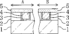
Below, with reference to figure 1 and Fig. 2, the semiconductor device with contrary fuse-wires structure that first embodiment of the present invention is related is described.
Fig. 1 is a major part profile, shows the structure of the semiconductor device with contrary fuse-wires structure that first embodiment of the present invention is related.Need mention, circuit has been shown among Fig. 1 form regional A and contrary fuse formation area B.
As shown in Figure 1, on Semiconductor substrate 1, form first dielectric film 2.On first dielectric film 2, formed first wiring (first metal pattern) 4 that contains first barrier film 3 by for example copper one-tenth.In first dielectric film 2 and first wiring 4, formed second barrier film 5.Here, second barrier film 5 has the effect of the metal diffusing that prevents to constitute first wiring 4, has been the effect of the nonproliferation film that prevents that copper from spreading here.Formed second dielectric film 6 on second barrier film 5.Formed second wiring (second metal pattern) 8 that for example is made of copper that contains the 3rd barrier film 7 on second dielectric film 6.
Here, form regional A at circuit, contain second wiring 8 of the 3rd barrier film 7, the connecting hole 9a that forms via running through second barrier film 5 is connected with first wiring 4; Form area B at contrary fuse,, make second barrier film 5 between it with contain first of first barrier film 3 and connect up between 4 with so contain second wiring 8 of the 3rd barrier film 7 because establish connecting hole for second barrier film 5.
After doing like this, form in the area B, in second barrier film of using as the nonproliferation film of the copper diffusion that prevents to constitute first wiring 45, formed contrary fuse 10 at contrary fuse.So contrary fuse 10 is caught from the metal of first wiring, 4 diffusions.Therefore, can utilize contrary fuse 10 to do easily owing to applying the contrary fuse usefulness that insulation breakdown takes place voltage.Particularly, in first wiring, 4 these embodiment that are made of copper, because copper is diffused in second barrier film 5 easily, so the contrary fuse that can use contrary fuse 10 to apply the easier generation insulation breakdown of voltage is used.
Fig. 2 shows a distortion of the structure of the semiconductor device shown in above-mentioned Fig. 1.Need mention, the part identical with component part among Fig. 1 represented with the symbol identical with Fig. 1.Below, be that the center is illustrated with the difference.
In semiconductor device shown in Figure 2, form area B at contrary fuse, on second barrier film 5, formed the stopple (second metal pattern) 12 that becomes by for example copper that contains the 3rd barrier film 11.In semiconductor device shown in Figure 1, form area B at contrary fuse and formed second wiring 8.This point is different.
Like this after forming stopple 12 on second barrier film 5, just can dwindle forming against the required area of fuse 10.
In addition, because make second barrier film 5 shown in Fig. 3 by using silicon nitride film (SiN) or carborundum (SiC) film, the effect of copper diffusion that prevents to constitute first wiring 4 is just big, so can realize the contrary fuse 10 that can set the voltage of the generation insulation breakdown that applied higher.
In addition, ideal situation is, forms area B at contrary fuse, and the surface of second barrier film 5 during than film forming is toward recessed, and second wiring 8 and 12 times calmnesses of stopple shown in Figure 2 shown in Figure 1 are formed on that negative area.Because as if making such structure, second barrier film 5 just causes insulation breakdown in second barrier film, 5 recessed parts easily, so can use contrary fuse 10 to do easily owing to applying the contrary fuse usefulness that insulation breakdown takes place voltage.
In this embodiment, explanation be that wiring or the used material of stopple are the sort of situation of copper, moreover, be exactly that the present invention also is enforceable under the situation of the material of making wiring or stopple with the noble metal such as for example gold or silver etc. beyond the copper.
(second embodiment)
Below, with reference to figure 3, the related semiconductor device with contrary fuse-wires structure of second embodiment of the present invention is described.
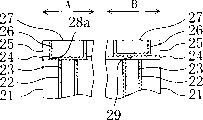
Fig. 3 is a major part profile, shows the structure of the semiconductor device with contrary fuse-wires structure that second embodiment of the present invention is related.
As shown in Figure 3, on first dielectric film 21 that is formed on the Semiconductor substrate (not shown), formed the stopple (first metal pattern) 23 that becomes by copper for example that contains first barrier film 22.On first dielectric film 21 and stopple 23, formed second barrier film 24.Here, second barrier film 24 works to prevent to constitute the nonproliferation film of the metal diffusing of stopple 23, has been the effect of the nonproliferation film of copper here.Formed second dielectric film 25 on second barrier film 24.Formed the wiring that for example is made of copper (second metal pattern) 27 that contains the 3rd barrier film 26 on second dielectric film 25.
Here, form regional A at circuit, contain the wiring 27 of the 3rd barrier film 26, the connecting hole 28a that forms via removing second barrier film 24 is connected with stopple 23; And form area B at contrary fuse, because second barrier film 24 is not established connecting hole, make second barrier film 24 between it with contain between the stopple 23 of first barrier film 22 so contain the wiring 27 of the 3rd barrier film 26.
After doing like this, form in the area B, in second barrier film of using as the film of the copper diffusion that prevents to constitute stopple 23 24, formed contrary fuse 29 at contrary fuse.So contrary fuse 29 is caught from the metal of stopple 23 diffusions.Therefore, can utilize contrary fuse 29 to do easily owing to applying the contrary fuse usefulness that insulation breakdown takes place voltage.Particularly, in this embodiment that stopple 23 is made of copper, because copper is diffused in second barrier film 24 easily, so the contrary fuse that can use contrary fuse 29 to apply the easier generation insulation breakdown of voltage is used.
Need mention, in this embodiment, explanation be the situation that on contrary fuse 29, is formed with wiring 27, but the same with described first embodiment, can be the structure of formation stopple (not shown) on contrary fuse 29.
After forming stopple on second barrier film 24, just can dwindle forming the contrary required area of fuse like this.
In addition, because make second barrier film 24 of Figure 1 and Figure 2 by using silicon nitride film (SiN) or carborundum (SiC) film, the effect of copper diffusion that prevents to constitute stopple 23 is just big, so can realize the contrary fuse 29 that can set the voltage of the generation insulation breakdown that applied higher.
In addition, ideal situation is: form area B at contrary fuse, the surface of second barrier film 24 during than film forming be toward recessed, wiring 27 shown in Figure 3 or replace wiring 27 and the stopple that forms sinks to that negative area.Because as if making such structure, second barrier film 24 just causes insulation breakdown in second barrier film, 24 recessed parts easily, so can use contrary fuse 29 to do easily owing to applying the contrary fuse usefulness that insulation breakdown takes place voltage.
In this embodiment, explanation be that wiring or the used material of stopple are the sort of situation of copper, moreover, be exactly that the present invention also is enforceable under the situation of the material of making wiring or stopple with the noble metal such as for example gold or silver etc. beyond the copper.
(the 3rd embodiment)
Below, with reference to figure 4 (a)~Fig. 4 (e), the manufacture method of the semiconductor device with contrary fuse-wires structure that the 3rd embodiment of the present invention is related is described.
Fig. 4 (a)~Fig. 4 (e) is the profile of an expression master operation, shows the manufacture method of the semiconductor device with contrary fuse-wires structure that the 3rd embodiment of the present invention is related.Need mention, among Fig. 4 with Fig. 1 in the common part of component part represent with the symbol identical with Fig. 1.
At first, shown in Fig. 4 (a), on Semiconductor substrate 1, form after first dielectric film 2, on this first dielectric film 2, form first wiring 4 that contains first barrier film 3 again by for example copper one-tenth.Then, in first dielectric film 2 and first wiring 4, form second barrier film 5.Second barrier film 5 works to prevent to constitute the nonproliferation film of the metal diffusing of first wiring 4, has been the effect of the nonproliferation film of copper here.And second barrier film 5 also plays etch stop film when forming the through hole on upper strata.
Then, shown in Fig. 4 (b), after forming second dielectric film 6 on second barrier film 5, on this second dielectric film 6, form through hole 30a and groove 31a again.Second dielectric film 6 can be formed in diverse a plurality of layer.And, as the situation that for example in the wiring of bottom, forms dielectric film etc., alleviate at needs under the situation of processing of ladder, can carry out planarization such as CMP technology.
Then, shown in Fig. 4 (c), form regional A at circuit, transference first wiring 4 is that the through hole 30a that lower-layer wiring connects exposes constant, form area B at contrary fuse simultaneously, forming corrosion-resisting pattern 32 so that first wiring 4 is not conveyed in covering is the through hole 30a that lower-layer wiring connects.
Then, shown in Fig. 4 (d), serve as that etching is carried out in shielding with corrosion-resisting pattern 32, in forming second barrier film 5 of regional A, circuit forms the connecting hole 9a that leads to first wiring 4.So, form regional A at circuit, through hole 30a is that lower-layer wiring is connected with first wiring 4 just.Afterwards, remove corrosion-resisting pattern 32.
Then, shown in Fig. 4 (e), form regional A at circuit, connecting hole 9a, through hole 30a and groove 31a form second wiring 8 by for example copper one-tenth that contains the 3rd barrier film 7, form area B at contrary fuse, through hole 30a and groove 31a form second wiring 8 by for example copper one-tenth that contains the 3rd barrier film 7.Can utilize sputtering technology, CVD technology or electroplating technology etc. to imbed metal material (for example being copper here) and afterwards, utilize the CMP technology to remove useless part again, form second wiring 8 like this.
Like this, in second barrier film 5, do not forming connecting hole with, second barrier film 5 is being connected up between 4 between first of it and first barrier film 3 so contain second wiring (metal pattern) 8 of the 3rd barrier film 7 because form in the area B at contrary fuse.In other words, form area B, form against fuse 10 at the lower floor that is arranged in second wiring 8 that is not connected, second barrier film 5 used as the film of the copper diffusion that prevents to constitute first wiring 4 with first wiring 4 at contrary fuse.
As mentioned above, according to embodiments of the invention, can utilize with the wiring of copper for example is that the damascene (damascene) of representative is that common wiring forms operation and forms contrary fuse 10.Therefore, at this moment needed operation road number just lacks than the road number that existing contrary fuse forms operation.The result is to reduce cost, to improve product percent of pass.
Need mention, in this embodiment, special explanation not done in the formation of through hole 30a, groove 31a in proper order, form through hole 30a earlier or form groove 31a earlier and all can.
Need mention, in this embodiment, second wiring 8 that is formed on the contrary fuse 10 that illustrates is the such structures that form in through hole 30a and the groove 31a by metal material is imbedded, moreover, even do not forming groove 31a, only form through hole 30a, on contrary fuse 10, only form under the situation of stopple, also can form contrary fuse 10.In this case, can dwindle the contrary fuse 10 necessary areas of formation.
In this embodiment, because make second barrier film 5 by using silicon nitride film (SiN) or carborundum (SiC) film, the effect of copper diffusion that prevents to constitute first wiring 4 is just big, so can realize the contrary fuse 10 that can set the voltage of the generation insulation breakdown that applied higher.
In addition, ideal situation is, forms area B at contrary fuse, and the surface of second barrier film 5 during than film forming is toward recessed, and second wiring 8 sinks to that negative area.Because as if making such structure, second barrier film 5 just causes insulation breakdown in second barrier film, 5 recessed parts easily, so can use contrary fuse 10 to do easily owing to applying the contrary fuse usefulness that insulation breakdown takes place voltage.
In this embodiment, explanation be that wiring or the used material of stopple are the sort of situation of copper, moreover, be exactly that the present invention also is enforceable under the situation of the material of making wiring or stopple with the noble metal such as for example gold or silver etc. beyond the copper.
(the 4th embodiment)
Below, with reference to figure 5 (a)~Fig. 5 (e), the manufacture method of the semiconductor device with contrary fuse-wires structure that the 4th embodiment of the present invention is related is described.
Fig. 5 (a)~Fig. 5 (e) is the profile of an expression master operation, shows the manufacture method of the semiconductor device with contrary fuse-wires structure that the 4th embodiment of the present invention is related.Need mention, the part identical with the component part shown in Fig. 1 represented with identical symbol among Fig. 5 (a)~Fig. 5 (e).
At first, shown in Fig. 5 (a), on Semiconductor substrate 1, form after first dielectric film 2, on this first dielectric film 2, form first wiring 4 that contains first barrier film 3 again by for example copper one-tenth.Then, in first dielectric film 2 and first wiring 4, form second barrier film 5.Second barrier film 5 works to prevent to constitute the nonproliferation film of the metal diffusing of first wiring 4, has been the effect of the nonproliferation film of copper here.And second barrier film 5 also plays etch stop film when forming the through hole on upper strata.
Then, shown in Fig. 5 (b), after forming second dielectric film 6 on second barrier film 5, on this second dielectric film 6, form through hole 30a again.Need mention, second dielectric film 6 can be formed in diverse a plurality of layer.And, as the situation that for example in the wiring of bottom, forms dielectric film etc., alleviate at needs under the situation of processing of ladder, can carry out planarization such as CMP technology.
Then, shown in Fig. 5 (c), form regional A at circuit, transference first wiring 4 is that the through hole 30a that lower-layer wiring connects exposes constant, form area B at contrary fuse simultaneously, forming corrosion-resisting pattern 33 so that first wiring 4 is not conveyed in covering with positive resist is the through hole 30a that lower-layer wiring connects.To accomplish when at this moment, forming corrosion-resisting pattern 33: be formed on not the same wide with the pattern width of groove and the width of through hole 30a on the through hole 30a that first wiring 4 connects.Or, layout is accomplished by the over half covering of positive erosion resistant with through hole 30a in order to the corrosion-resisting pattern that forms groove, make the positive erosion resistant of the remaining inadequately next part of exposure in the through hole 30a like this, form corrosion-resisting pattern 33 by the positive erosion resistant of that part under the remnants at last.Here, the pattern width of formed groove is than the big 0.2 μ m of pattern width of through hole.
Then, shown in Fig. 5 (d), be that shielding is carried out etching and formed groove 31a with corrosion-resisting pattern 33.At this moment,, in second barrier film 5, form this second barrier film 5 of break-through and lead to the connecting hole 9a of first wiring 4, be connected so the through hole 30a and first wiring 4 are the wiring of lower floor because form among the regional A at circuit.Afterwards, remove corrosion-resisting pattern 33.
Then, shown in Fig. 5 (e), form regional A at circuit, form second wiring (metal pattern) 8 that contains the 3rd barrier film 7 at connecting hole 9a, through hole 30a and groove 31a by for example copper one-tenth, form area B at contrary fuse, form second wiring 8 that contains the 3rd barrier film 7 by for example copper one-tenth at through hole 30a and groove 31a.Can utilize sputtering technology, CVD technology or electroplating technology etc. to imbed metal material (for example being copper here) and afterwards, utilize the CMP technology to remove useless part again, form second wiring 8 like this.
Like this, in second barrier film 5, do not forming connecting hole with, making second barrier film 5 between it with contain first of first barrier film 3 and connect up between 4 so contain second wiring 8 of the 3rd barrier film 7 because form in the area B at contrary fuse.In other words, form area B, form against fuse 10 at the lower floor that is arranged in second wiring 8 that is not connected, second barrier film 5 used as the film of the copper diffusion that prevents to constitute first wiring 4 with first wiring 4 at contrary fuse.
As mentioned above, according to the manufacture method of the related semiconductor device of this embodiment, can utilize with the wiring of copper for example is that the damascene operation of representative is that common wiring forms operation and forms contrary fuse 10.Therefore, at this moment needed operation road number just lacks than the road number that existing contrary fuse forms operation.The result is to reduce cost, to improve product percent of pass.
Need mention, in this embodiment, special explanation not done in the formation of through hole 30a, groove 31a in proper order, form through hole 30a earlier or form groove 31a earlier and all can.
Need mention, in this embodiment, second wiring 8 that is formed on the contrary fuse 10 that illustrates is the such structures that form in through hole 30a and the groove 31a by metal material is imbedded, moreover, even do not forming groove 31a, only form through hole 30a, on contrary fuse 10, only form under the situation of stopple, also can form contrary fuse 10.In this case, can dwindle the contrary fuse 10 necessary areas of formation.
In this embodiment, because make second barrier film 5 by using silicon nitride film (SiN) or carborundum (SiC) film, the effect of copper diffusion that prevents to constitute first wiring 4 is just big, so can realize the contrary fuse 10 that can set the voltage of the generation insulation breakdown that applied higher.
In addition, ideal situation is, the surface when contrary fuse forms second barrier film 5 that area B should the zone than film forming is toward recessed, and second wiring 8 sinks to that negative area.Because as if making such structure, second barrier film 5 just causes insulation breakdown in second barrier film, 5 recessed parts easily, so can use contrary fuse 10 to do easily owing to applying the contrary fuse usefulness that insulation breakdown takes place voltage.
In this embodiment, explanation be that wiring or the used material of stopple are the sort of situation of copper, moreover, be exactly that the present invention also is enforceable under the situation of the material of making wiring or stopple with the noble metal such as for example gold or silver etc. beyond the copper.
(the 5th embodiment)
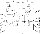
Below, with reference to figure 6 (a)~Fig. 6 (d), the manufacture method of the semiconductor device with contrary fuse-wires structure that the 5th embodiment of the present invention is related is described.
Fig. 6 (a)~Fig. 6 (d) is the profile of an expression master operation, shows the manufacture method of the semiconductor device with contrary fuse-wires structure that the 5th embodiment of the present invention is related.Need mention, the part identical with the component part shown in Fig. 1 represented with identical symbol among Fig. 6 (a)~Fig. 6 (d).
At first, shown in Fig. 6 (a), on Semiconductor substrate 1, form after first dielectric film 2, on this first dielectric film 2, form first wiring 4 that contains first barrier film 3 again by for example copper one-tenth.Then, in first dielectric film 2 and first wiring 4, form second barrier film 5.Second barrier film 5 works to prevent to constitute the nonproliferation film of the metal diffusing of first wiring 4, has been the effect of the nonproliferation film of copper here.And second barrier film 5 also plays etch stop film when forming the through hole on upper strata.
Then, shown in Fig. 6 (b), on second barrier film 5 of contrary fuse formation area B, form corrosion-resisting pattern 34.Serve as that etching is carried out in shielding with corrosion-resisting pattern 34 again, it is thinner to allow circuit form the thickness of second barrier film 5 among the regional A.Remove corrosion-resisting pattern 34 afterwards again.
Then, shown in Fig. 6 (c), after forming second dielectric film 6 on second barrier film 5, on this second dielectric film 6, form through hole 30a again.Need mention, second dielectric film 6 can be formed in diverse a plurality of layer.And, as the situation that for example in the wiring of bottom, forms dielectric film etc., alleviate at needs under the situation of processing of ladder, can carry out planarization such as CMP technology.
Then, shown in Fig. 6 (d), etching second dielectric film 6 and form groove 31a.At this moment, because the thickness that forms second barrier film 5 among the regional A at circuit has approached, so second barrier film 5 that will expose from the bottom of through hole 30a by etching is removed fully, come to form connecting hole 9a like this in second barrier film 5, through hole 30a leads to first wiring 4.On the other hand, form area B, because the thickness of second barrier film 5 is thick, so even second barrier film 5 that will expose from the bottom of through hole 30a by etching is removed, through hole 30a is also logical less than first wiring 4 at contrary fuse.
Then, shown in Fig. 6 (e), form regional A at circuit, form second wiring (metal pattern) 8 that contains the 3rd barrier film 7 at connecting hole 9a, through hole 30a and groove 31a by for example copper one-tenth, form area B at contrary fuse, form second wiring 8 that contains the 3rd barrier film 7 by for example copper one-tenth at through hole 30a and groove 31a.Can utilize sputtering technology, CVD technology or electroplating technology etc. to imbed metal material (for example being copper here) and afterwards, utilize the CMP technology to remove useless part again, form second wiring 8 like this.
Like this, in second barrier film 5, do not forming connecting hole with, making second barrier film 5 between it with contain first of first barrier film 3 and connect up between 4 so contain second wiring 8 of the 3rd barrier film 7 because form in the area B at contrary fuse.In other words, form area B, form against fuse 10 at the lower floor that is arranged in second wiring 8 that is not connected, second barrier film 5 used as the film of the copper diffusion that prevents to constitute first wiring 4 with first wiring 4 at contrary fuse.
As mentioned above, according to embodiments of the invention, can utilize common wiring to form operation is that the damascene operation of representative forms contrary fuse 10 with for example copper wiring promptly.Therefore, at this moment needed operation road number just lacks than the road number that existing contrary fuse forms operation.The result is to reduce cost, to improve product percent of pass.
Need mention, in this embodiment, special explanation not done in the formation of through hole 30a, groove 31a in proper order, form through hole 30a earlier or form groove 31a earlier and all can.
Need mention, in this embodiment, second wiring 8 that is formed on the contrary fuse 10 that illustrates is the such structures that form in through hole 30a and the groove 31a by metal material is imbedded, moreover, even do not forming groove 31a, only form through hole 30a, on contrary fuse 10, only form under the situation of stopple, also can form contrary fuse 10.In this case, can dwindle the area that contrary fuse forms area B.
In this embodiment, because make second barrier film 5 by using silicon nitride film (SiN) or carborundum (SiC) film, the effect of copper diffusion that prevents to constitute first wiring 4 is just big, so can realize the contrary fuse 10 that can set the voltage of the generation insulation breakdown that applied higher.
In addition, ideal situation is, forms area B at contrary fuse, and the surface of second barrier film 5 during than film forming is toward recessed, and second wiring 8 sinks to that negative area.Because as if making such structure, second barrier film 5 just causes insulation breakdown in second barrier film, 5 recessed parts easily, so can use contrary fuse 10 to do easily owing to applying the contrary fuse usefulness that insulation breakdown takes place voltage.
In this embodiment, explanation be that wiring or the used material of stopple are the sort of situation of copper, moreover, be exactly that the present invention also is enforceable under the situation of the material of making wiring or stopple with the noble metal such as for example gold or silver etc. beyond the copper.
(the 6th embodiment)
Below, with reference to figure 7 (a)~Fig. 7 (f), the manufacture method of the semiconductor device with contrary fuse-wires structure that the 6th embodiment of the present invention is related is described.
Fig. 7 (a)~Fig. 7 (f) is the profile of an expression master operation, shows the manufacture method of the semiconductor device with contrary fuse-wires structure that the 6th embodiment of the present invention is related.Need mention, the part identical with the component part shown in Fig. 1 represented with identical symbol among Fig. 7 (a)~Fig. 7 (f).
At first, shown in Fig. 7 (a), on Semiconductor substrate 1, form after first dielectric film 2, on this first dielectric film 2, form first wiring 4 that contains first barrier film 3 again by for example copper one-tenth.Then, in first dielectric film 2 and first wiring 4, form second barrier film 5.Second barrier film 5 works to prevent to constitute the nonproliferation film of the metal diffusing of first wiring 4, has been the effect of the nonproliferation film of copper here.And second barrier film 5 also plays etch stop film when forming the through hole on upper strata.Then, on second barrier film 5, form second dielectric film 35 and the 3rd dielectric film 36 more successively.
Then, shown in Fig. 7 (b), on the 3rd dielectric film 36 of contrary fuse formation area B, form corrosion-resisting pattern 37.Be that shielding is carried out etching and the 3rd dielectric film 36 that circuit forms among the regional A is removed with corrosion-resisting pattern 37 again.Remove corrosion-resisting pattern 37 afterwards again.
Then, shown in Fig. 7 (c), form among the regional A at circuit and on second dielectric film 35, to form the 4th dielectric film 38, form at contrary fuse and form the 4th dielectric film 38 on area B the 3rd dielectric film 36.
Then, shown in Fig. 7 (d), form among the regional A, in second dielectric film 35 and the 4th dielectric film 38, form this second dielectric film 35 of break-through and the 4th dielectric film 38 and extending and leading to the through hole 30a of second barrier film 5 at circuit.On the other hand, form the through hole 30a that forms break-through the 4th dielectric film 38 on the 4th dielectric film 38 in the area B and extending and leading to the 3rd dielectric film 36 at contrary fuse.In this case, the 3rd dielectric film 36 plays etch stop film.
Then, shown in Fig. 7 (e), etching the 4th dielectric film 38 and form groove 31a.At this moment, form among the regional A at circuit, remove by second barrier film 5 that etching will be exposed from the bottom of through hole 30a, and form connecting hole 9a in second barrier film 5, through hole 30a leads to first wiring 4.On the other hand, form area B, remove the 3rd dielectric film 36 and second dielectric film 35, and allow second barrier film 5 expose from the bottom of through hole 30a at contrary fuse.
Then, shown in Fig. 7 (f), form among the regional A, form second wiring (metal pattern) 8 that contains the 3rd barrier film 7 by for example copper one-tenth at connecting hole 9a, through hole 30a and groove 31a at circuit; Form area B at contrary fuse, form second wiring 8 that contains the 3rd barrier film 7 by for example copper one-tenth at through hole 30a and groove 31a.Can utilize sputtering technology, CVD technology or electroplating technology etc. to imbed metal material (for example being copper here) and afterwards, utilize the CMP technology to remove useless part again, form second wiring 8 like this.
Like this, in second barrier film 5, do not forming connecting hole with, making second barrier film 5 between it with contain first of first barrier film 3 and connect up between 4 so contain second wiring 8 of the 3rd barrier film 7 because form in the area B at contrary fuse.In other words, form area B, form against fuse 10 at the lower floor that is arranged in second wiring 8 that is not connected, second barrier film 5 used as the film of the copper diffusion that prevents to constitute first wiring 4 with first wiring 4 at contrary fuse.
As mentioned above, according to the manufacture method of the semiconductor device of present embodiment, can utilize with for example copper wiring is that the damascene operation of representative is that common wiring forms operation and forms contrary fuse 10.Therefore, at this moment needed operation road number just lacks than the road number that existing contrary fuse forms operation.The result is to reduce cost, to improve product percent of pass.
Need mention, in this embodiment, special explanation not done in the formation of through hole 30a, groove 31a in proper order, form through hole 30a earlier or form groove 31a earlier and all can.
Need mention, in this embodiment, second wiring 8 that is formed on the contrary fuse 10 that illustrates is the such structures that form in through hole 30a and the groove 31a by metal material is imbedded, moreover, even do not forming groove 31a, only form through hole 30a, on contrary fuse 10, only form under the situation of stopple, also can form contrary fuse 10.In this case, can dwindle the contrary fuse 10 needed areas of formation.
In this embodiment, because make second barrier film 5 by using silicon nitride film (SiN) or carborundum (SiC) film, the effect of copper diffusion that prevents to constitute first wiring 4 is just big, so can realize the contrary fuse 10 that can set the voltage of the generation insulation breakdown that applied higher.
In addition, ideal situation is, forms area B at contrary fuse, and the surface of second barrier film 5 during than film forming is toward recessed, and second wiring 8 sinks to that negative area.Because as if making such structure, second barrier film 5 just causes insulation breakdown in second barrier film, 5 recessed parts easily, so can use contrary fuse 10 to do easily owing to applying the contrary fuse usefulness that insulation breakdown takes place voltage.
In this embodiment, explanation be that wiring or the used material of stopple are the sort of situation of copper, moreover, be exactly that the present invention also is enforceable under the situation of the material of making wiring or stopple with the noble metal such as for example gold or silver etc. beyond the copper.
(the 7th embodiment)
Below, with reference to figure 8 (a)~Fig. 8 (e), the manufacture method of the semiconductor device with contrary fuse-wires structure that the 7th embodiment of the present invention is related is described.
Fig. 8 (a)~Fig. 8 (e) is the profile of an expression master operation, shows the manufacture method of the semiconductor device with contrary fuse-wires structure that the 7th embodiment of the present invention is related.Need mention, the part identical with the component part shown in Fig. 3 represented with identical symbol among Fig. 8 (a)~Fig. 8 (e).
Shown in Fig. 8 (a), on Semiconductor substrate (not shown) for example, form after first dielectric film 21, on this first dielectric film 21, form the stopple 23 that becomes by for example copper that contains first barrier film 22 again.Then, on first dielectric film 21 and stopple 23, form second barrier film 24.Here, second barrier film 24 works to prevent to constitute the nonproliferation film of the metal diffusing of stopple 23, has been the effect of the nonproliferation film of copper here.And second barrier film 24 plays etch stop film when forming the through hole on upper strata.
Then, shown in Fig. 8 (b), after forming second dielectric film 25 on second barrier film 24, form at circuit again and form groove 29a among the regional A on second dielectric film 25.On the other hand, form in the area B, on second dielectric film 25, form through hole 40a at contrary fuse.
Then, shown in Fig. 8 (c), form corrosion-resisting pattern 41 so that the through hole 40a that will be formed in the contrary fuse formation area B covers.
Then, shown in Fig. 8 (d), be that shielding is carried out etching and will be removed from being formed on second barrier film 24 that bottom that circuit forms the groove 39a the regional A exposes with corrosion-resisting pattern 41, and form connecting hole 28a, allow stopple 23 expose.Afterwards, remove corrosion-resisting pattern 41 again.
Then, shown in Fig. 8 (e), form among the regional A at circuit, form the wiring (metal pattern) 27 that becomes by for example copper contain the 3rd barrier film 26 at connecting hole 28a, groove 39a, form at contrary fuse simultaneously and form stopple (metal pattern) 27b that becomes by for example copper that contains the 3rd barrier film 26b among the area B through hole 40a.Can utilize sputtering technology, CVD technology or electroplating technology etc. to imbed metal material (for example being copper here) and afterwards, utilize the CMP technology to remove useless part again, form wiring 27 and 27b like this.
Like this, in second barrier film 24, do not forming connecting hole, making second barrier film 24 between it with contain between the stopple 23 of first barrier film 22 so contain the stopple 27b of the 3rd barrier film 26b because form in the area B at contrary fuse.In other words, form area B, form against fuse 29b at the lower floor that is arranged in the stopple 27b that is not connected, second barrier film 24 used as the film of the copper diffusion that prevents to constitute stopple 23 with stopple 23 at contrary fuse.
As mentioned above, according to the manufacture method of the related semiconductor device of this embodiment, can utilize with the wiring of copper for example is that the damascene operation of representative is that common wiring forms operation and forms contrary fuse 29b.Therefore, at this moment needed operation road number just lacks than the road number that existing contrary fuse forms operation.The result is to reduce cost, to improve product percent of pass.
Need mention, in this embodiment, explanation be the situation that on contrary fuse 29b, forms stopple 27b, moreover the same with Fig. 3 among described second embodiment, also can on contrary fuse 29b, form the such structure of wiring.But, comparing with structure shown in Figure 3, it is littler to form the required area of contrary fuse among this embodiment.
In this embodiment, because make second barrier film 24 by using silicon nitride film (SiN) or carborundum (SiC) film, the effect of copper diffusion that prevents to constitute stopple 23 is just big, so can realize the contrary fuse 29b that can set the voltage of the generation insulation breakdown that applied higher.
In addition, ideal situation is: form area B at contrary fuse, the surface of second barrier film 24 during than film forming is toward recessed, and stopple 27b sinks to that negative area.Because as if making such structure, second barrier film 24 just causes insulation breakdown in the recessed part of stopple 27b easily, so can use contrary fuse 29b to do easily owing to applying the contrary fuse usefulness that insulation breakdown takes place voltage.
In this embodiment, explanation be that wiring or the used material of stopple are the sort of situation of copper, moreover, be exactly that the present invention also is enforceable under the situation of the material of making wiring or stopple with the noble metal such as for example gold or silver etc. beyond the copper.
-practicality-
In sum, the present invention is suitable for semiconductor devices and manufacture method thereof. Be particularly suitable at structure again The logic element that becomes is used in FPGA (the Field Programmable Gate Array) element Contrary fuse-wires structure and manufacture method thereof.
Claims (19)
1. semiconductor device is characterized in that:
Comprise:
Be formed on the Semiconductor substrate by first metal first metal pattern,
Be formed on the dielectric film on described first metal pattern, and
Be formed on the described dielectric film by second metal second metal pattern;
Described dielectric film has for preventing the block of described first metal diffusing.
2. semiconductor device according to claim 1 is characterized in that:
Contain described first metal that diffusion comes in the described dielectric film.
3. semiconductor device according to claim 1 is characterized in that:
Described second metal pattern forms the appearance that sinks in the described dielectric film.
4. semiconductor device according to claim 1 is characterized in that:
Described first metal pattern is wiring or stopple.
5. semiconductor device according to claim 1 is characterized in that:
Described second metal pattern is wiring or stopple.
6. semiconductor device is characterized in that:
Comprise:
Be formed on the Semiconductor substrate by first metal first metal pattern,
Be formed on the dielectric film on described first metal pattern, and
Be formed on the described dielectric film by second metal second metal pattern;
Described dielectric film has for preventing the block of described first metal diffusing;
Described second metal pattern forms: form described dielectric film of regional break-through and the described first metal pattern conducting at circuit, simultaneously form the zone at contrary fuse and make described dielectric film between between it and described first metal pattern.
7. semiconductor device according to claim 6 is characterized in that:
Contain described first metal that has spread in the described dielectric film.
8. semiconductor device according to claim 6 is characterized in that:
Described contrary fuse forms described second metal pattern in the zone, forms the appearance that sinks in the described dielectric film.
9. semiconductor device according to claim 6 is characterized in that:
Described first metal pattern is wiring or stopple.
10. semiconductor device according to claim 6 is characterized in that:
Described second metal pattern is wiring or stopple.
11. the manufacture method of a semiconductor device is characterized in that:
Comprise:
On Semiconductor substrate, form step by the first metal wiring,
In described wiring, form the step of first dielectric film,
On described first dielectric film, form the step of second dielectric film,
Circuit form zone and contrary fuse form form respectively on second dielectric film described in the zone be positioned at described wiring above allow the step of the opening portion that described first dielectric film exposes simultaneously,
Forming corrosion-resisting pattern forms after the described opening portion in zone to cover described contrary fuse, do shielding with this corrosion-resisting pattern again and carry out etching, and described first dielectric film that expose the bottom of described opening portion that forms the zone from described circuit removed and the step that allows described wiring expose, and
Remove after the described corrosion-resisting pattern, form that the described opening portion in zone and described opening portion that described contrary fuse forms the zone are imbedded second metal respectively and the step that forms metal pattern at described circuit;
Described first dielectric film has the block that prevents described first metal diffusing.
12. the manufacture method of a semiconductor device is characterized in that:
Comprise:
On Semiconductor substrate, form step by the first metal wiring,
In described wiring, form the step of first dielectric film,
On described first dielectric film, form the step of second dielectric film,
Circuit form zone and contrary fuse form form respectively on second dielectric film described in the zone be positioned at described wiring above allow the step of first opening portion that described first dielectric film exposes simultaneously,
Forming for when forming the photoresistance pattern that forms by the eurymeric photoresistance of second opening portion on the described top that forms described first opening portion in zone against fuse, so that the nubbin of the described eurymeric photoresistance that forms serves as to shield to carry out etching by exposing inadequately, form the step that described first dielectric film that exposes from the bottom of described first opening portion in the zone allows described wiring expose and remove described circuit, and
Remove after the described corrosion-resisting pattern, form that described first opening portion in zone and described first opening portion that described contrary fuse forms the zone are imbedded second metal respectively and the step that forms metal pattern at described circuit;
Described first dielectric film has the block that prevents described first metal diffusing.
13. the manufacture method of a semiconductor device is characterized in that:
Comprise:
On Semiconductor substrate, form step by the first metal wiring,
In described wiring, form the step of first dielectric film,
Carry out etching and will be present in the step that circuit forms the part filming in zone in described first dielectric film;
Described carry out etched step after, on described first dielectric film, form the step of second dielectric film,
Circuit form form on described second dielectric film in zone be positioned at described wiring above and the opening portion that allows described wiring expose, simultaneously contrary fuse form form on described second dielectric film in zone be positioned at described wiring above and allow the step of the opening portion that described first dielectric film exposes, and
Form that the described opening portion in zone and described opening portion that described contrary fuse forms the zone are imbedded second metal respectively and the step that forms metal pattern at described circuit;
Described first dielectric film has the block that prevents described first metal diffusing.
14. the manufacture method of a semiconductor device is characterized in that:
Comprise:
On Semiconductor substrate, form step by the first metal wiring,
In described wiring, form the step of first dielectric film,
On described first dielectric film, form the step of second dielectric film,
On described second dielectric film, form the step of the 3rd dielectric film,
Carry out etching and form the step that regional part is removed being present in circuit in described the 3rd dielectric film,
Described carry out etched step after, on described second dielectric film and described the 3rd dielectric film, form the step of the 4th dielectric film,
Circuit form form on zone described the 4th dielectric film, described second dielectric film and described first dielectric film be positioned at described wiring above and the opening portion that allows described wiring expose, simultaneously contrary fuse form form on described the 4th dielectric film in zone, described the 3rd dielectric film and described second dielectric film be positioned at described wiring above and allow the step of the opening portion that described first dielectric film exposes, and
Form that the described opening portion in zone and described opening portion that described contrary fuse forms the zone are imbedded second metal respectively and the step that forms metal pattern at described circuit;
Described first dielectric film has the block that prevents described first metal diffusing.
15. the manufacture method according to the described semiconductor device of arbitrary claim in the claim 11~14 is characterized in that:
The step of described formation opening portion is for forming the step of wiring trench or through hole;
In the step of described formation opening portion, form under the situation of described wiring trench, the step of described formation metal pattern is for forming the step of wiring, and in the step of described formation opening portion, form under the situation of described through hole, the step of described formation metal pattern is for forming the step of stopple.
16. the manufacture method of a semiconductor device is characterized in that:
Comprise:
On Semiconductor substrate, form step by the first metal stopple,
On described stopple, form the step of first dielectric film,
On described first dielectric film, form the step of second dielectric film,
Circuit form zone and contrary fuse form form respectively on second dielectric film described in the zone be positioned at described stopple above allow the step of the opening portion that described first dielectric film exposes simultaneously,
Forming corrosion-resisting pattern is formed on described contrary fuse with covering and forms after the described opening portion in zone, do shielding with this corrosion-resisting pattern again and carry out etching, and described circuit is formed that described first dielectric film that exposes from the bottom of described opening portion in the zone is removed and the step that allows described stopple expose, and
Remove after the described corrosion-resisting pattern, form that the described opening portion in zone and described opening portion that described contrary fuse forms the zone are imbedded second metal respectively and the step that forms metal pattern at described circuit;
Described first dielectric film has the block that prevents described first metal diffusing.
17. the manufacture method of semiconductor device according to claim 16 is characterized in that:
The step of described formation opening portion is for forming the step of wiring trench or through hole;
In the step of described formation opening portion, form under the situation of described wiring trench, the step of described formation metal pattern is for forming the step of wiring, and in the step of described formation opening portion, form under the situation of through hole, the step of described formation metal pattern is for forming the step of stopple.
18. the manufacture method according to claim 11,12,13,14 or 16 described semiconductor device is characterized in that:
Described first dielectric film contains described first metal that diffusion comes.
19. the manufacture method according to claim 11,12,13,14 or 16 described semiconductor device is characterized in that:
The described metal pattern that is formed on described first dielectric film forms the appearance that sinks in the described dielectric film.
Applications Claiming Priority (2)
| Application Number | Priority Date | Filing Date | Title |
|---|---|---|---|
| JP2003192675 | 2003-07-07 | ||
| JP2003192675 | 2003-07-07 |
Publications (1)
| Publication Number | Publication Date |
|---|---|
| CN1577832A true CN1577832A (en) | 2005-02-09 |
Family
ID=33562419
Family Applications (1)
| Application Number | Title | Priority Date | Filing Date |
|---|---|---|---|
| CNA2004100621554A Pending CN1577832A (en) | 2003-07-07 | 2004-07-05 | Semiconductor device and method for fabricating the same |
Country Status (3)
| Country | Link |
|---|---|
| US (2) | US20050006773A1 (en) |
| CN (1) | CN1577832A (en) |
| TW (1) | TW200504935A (en) |
Families Citing this family (3)
| Publication number | Priority date | Publication date | Assignee | Title |
|---|---|---|---|---|
| JP5139689B2 (en) * | 2007-02-07 | 2013-02-06 | セイコーインスツル株式会社 | Semiconductor device and manufacturing method thereof |
| CN105452547B (en) * | 2013-08-15 | 2018-03-20 | 沙特基础全球技术有限公司 | Shear spinning sub-micron fibers |
| US10270075B2 (en) | 2015-07-09 | 2019-04-23 | E I Du Pont De Nemours And Company | Separator having adhesive layer, manufacturing method of the same, and electrochemical device having the same |
Family Cites Families (15)
| Publication number | Priority date | Publication date | Assignee | Title |
|---|---|---|---|---|
| US5272101A (en) * | 1990-04-12 | 1993-12-21 | Actel Corporation | Electrically programmable antifuse and fabrication processes |
| US5602053A (en) * | 1996-04-08 | 1997-02-11 | Chartered Semidconductor Manufacturing Pte, Ltd. | Method of making a dual damascene antifuse structure |
| US6025226A (en) * | 1998-01-15 | 2000-02-15 | International Business Machines Corporation | Method of forming a capacitor and a capacitor formed using the method |
| US6021079A (en) * | 1998-05-13 | 2000-02-01 | Richard Mann | Fast, low cost method of developing code for contact programmable ROMs |
| US6515343B1 (en) * | 1998-11-19 | 2003-02-04 | Quicklogic Corporation | Metal-to-metal antifuse with non-conductive diffusion barrier |
| US6251710B1 (en) * | 2000-04-27 | 2001-06-26 | International Business Machines Corporation | Method of making a dual damascene anti-fuse with via before wire |
| WO2002029892A2 (en) * | 2000-10-03 | 2002-04-11 | Broadcom Corporation | High-density metal capacitor using dual-damascene copper interconnect |
| US6809398B2 (en) * | 2000-12-14 | 2004-10-26 | Actel Corporation | Metal-to-metal antifuse structure and fabrication method |
| JP2002305242A (en) * | 2001-04-05 | 2002-10-18 | Canon Sales Co Inc | Method for manufacturing semiconductor device |
| US6541792B1 (en) * | 2001-09-14 | 2003-04-01 | Hewlett-Packard Development Company, Llp | Memory device having dual tunnel junction memory cells |
| US6943065B2 (en) * | 2002-03-25 | 2005-09-13 | Micron Technology Inc. | Scalable high performance antifuse structure and process |
| JP3590034B2 (en) * | 2002-04-26 | 2004-11-17 | Necエレクトロニクス株式会社 | Semiconductor capacitive element and manufacturing method thereof |
| US6709918B1 (en) * | 2002-12-02 | 2004-03-23 | Chartered Semiconductor Manufacturing Ltd. | Method for making a metal-insulator-metal (MIM) capacitor and metal resistor for a copper back-end-of-line (BEOL) technology |
| JP3811473B2 (en) * | 2003-02-25 | 2006-08-23 | 富士通株式会社 | Semiconductor device |
| US20050035429A1 (en) * | 2003-08-15 | 2005-02-17 | Yeh Chih Chieh | Programmable eraseless memory |
-
2004
- 2004-07-05 CN CNA2004100621554A patent/CN1577832A/en active Pending
- 2004-07-07 US US10/884,998 patent/US20050006773A1/en not_active Abandoned
- 2004-07-07 TW TW093120396A patent/TW200504935A/en unknown
-
2006
- 2006-11-17 US US11/600,844 patent/US20070057376A1/en not_active Abandoned
Also Published As
| Publication number | Publication date |
|---|---|
| US20050006773A1 (en) | 2005-01-13 |
| TW200504935A (en) | 2005-02-01 |
| US20070057376A1 (en) | 2007-03-15 |
Similar Documents
| Publication | Publication Date | Title |
|---|---|---|
| CN1096116C (en) | Semiconductor device and manufacturing method thereof | |
| CN1956173A (en) | Semiconductor device and method of manufacture thereof | |
| CN1835226A (en) | Semiconductor device and manufacturing process therefor | |
| CN1870857A (en) | Shielded electronic circuit unit and method of manufacturing the same | |
| CN1855467A (en) | Semiconductor device and method of manufacturing same | |
| CN1135618C (en) | Semi-conductor apparatus and its producing method | |
| CN1819157A (en) | Semiconductor device | |
| CN1967800A (en) | Process for producing semiconductor integrated circuit device | |
| CN1832132A (en) | Semiconductor device and method of manufacturing the same | |
| CN1645607A (en) | Semiconductor device and method for fabricating the same | |
| CN101066005A (en) | Multilayer wiring board and method for manufacturing same | |
| CN1670953A (en) | Semiconductor device | |
| CN1701418A (en) | Semiconductor device producing method, semiconductor wafer and semiconductor device | |
| CN1722370A (en) | The manufacture method of semiconductor device | |
| CN1499595A (en) | Semiconductor device and its mfg. method | |
| CN1901162A (en) | Method for fabricating a circuitry component by continuous electroplating and circuitry component structure | |
| CN1722414A (en) | Semiconductor device and manufacture method thereof | |
| CN1957464A (en) | Semiconductor device, wiring board and manufacturing method thereof | |
| CN1842903A (en) | Semiconductor device and method for fabricating same | |
| CN1444279A (en) | Semiconductor device and its mfg. method | |
| CN1604293A (en) | Method for manufacturing semiconductor device and semiconductor device | |
| CN1118095C (en) | Fabrication method of semiconductor device using CMP process | |
| CN1779967A (en) | Semiconductor device including metal-insulator-metal capacitor arrangement | |
| CN1302534C (en) | Semiconductor device with multilayer wiring layers and its mfg. method | |
| CN1893034A (en) | Semiconductor device |
Legal Events
| Date | Code | Title | Description |
|---|---|---|---|
| C06 | Publication | ||
| PB01 | Publication | ||
| C10 | Entry into substantive examination | ||
| SE01 | Entry into force of request for substantive examination | ||
| AD01 | Patent right deemed abandoned | ||
| C20 | Patent right or utility model deemed to be abandoned or is abandoned |