CN1574401A - Optical receiver, optical transmitter and optical transceiver - Google Patents

Optical receiver, optical transmitter and optical transceiver Download PDF

Info

Publication number
CN1574401A
CN1574401A CNA2004100473139A CN200410047313A CN1574401A CN 1574401 A CN1574401 A CN 1574401A CN A2004100473139 A CNA2004100473139 A CN A2004100473139A CN 200410047313 A CN200410047313 A CN 200410047313A CN 1574401 A CN1574401 A CN 1574401A
Authority
CN
China
Prior art keywords
light
receiving device
receiving
mentioned
optical
Prior art date
Legal status (The legal status is an assumption and is not a legal conclusion. Google has not performed a legal analysis and makes no representation as to the accuracy of the status listed.)
Pending
Application number
CNA2004100473139A
Other languages
Chinese (zh)
Inventor
岛田和宏
池田麻子
佐仓成之
Current Assignee (The listed assignees may be inaccurate. Google has not performed a legal analysis and makes no representation or warranty as to the accuracy of the list.)
Toshiba Corp
Original Assignee
Toshiba Corp
Priority date (The priority date is an assumption and is not a legal conclusion. Google has not performed a legal analysis and makes no representation as to the accuracy of the date listed.)
Filing date
Publication date
Priority claimed from JP2003154910A external-priority patent/JP2004357158A/en
Priority claimed from JP2003154934A external-priority patent/JP3742403B2/en
Application filed by Toshiba Corp filed Critical Toshiba Corp
Publication of CN1574401A publication Critical patent/CN1574401A/en
Pending legal-status Critical Current

Links

Images

Classifications

    • HELECTRICITY
    • H04ELECTRIC COMMUNICATION TECHNIQUE
    • H04BTRANSMISSION
    • H04B10/00Transmission systems employing electromagnetic waves other than radio-waves, e.g. infrared, visible or ultraviolet light, or employing corpuscular radiation, e.g. quantum communication
    • H04B10/50Transmitters
    • H04B10/501Structural aspects
    • H04B10/503Laser transmitters
    • HELECTRICITY
    • H04ELECTRIC COMMUNICATION TECHNIQUE
    • H04BTRANSMISSION
    • H04B10/00Transmission systems employing electromagnetic waves other than radio-waves, e.g. infrared, visible or ultraviolet light, or employing corpuscular radiation, e.g. quantum communication
    • H04B10/60Receivers
    • H04B10/66Non-coherent receivers, e.g. using direct detection
    • H04B10/69Electrical arrangements in the receiver

Landscapes

  • Physics & Mathematics (AREA)
  • Electromagnetism (AREA)
  • Engineering & Computer Science (AREA)
  • Computer Networks & Wireless Communication (AREA)
  • Signal Processing (AREA)
  • Optics & Photonics (AREA)
  • Light Receiving Elements (AREA)
  • Photo Coupler, Interrupter, Optical-To-Optical Conversion Devices (AREA)

Abstract

本发明的光接收机具备:第1受光器件,用来将光信号向电信号进行变换并将该电信号从一端予以输出;受光器件列,由多个第2受光器件构成,该第2受光器件与上述第1受光器件的另一端连接以向上述第1受光器件供给电力,并且相互串联连接。光发送机具备:表面发光型发光器件,用来将电信号变换成光信号对并发送该光信号;受光器件列,由多个受光器件构成,该受光器件用来从上述发光器件接受光的照射以产生电力并且相互串联连接,从上述发光器件上面所放射的光作为光信号加以使用,从上述发光器件内面所放射的光照射到上述受光器件列。

Figure 200410047313

The optical receiver of the present invention includes: a first light receiving device for converting an optical signal into an electrical signal and outputting the electrical signal from one end; The device is connected to the other end of the first light receiving device to supply power to the first light receiving device, and is connected in series with each other. The optical transmitter has: a surface-emitting light-emitting device for converting an electrical signal into an optical signal pair and transmitting the optical signal; a light-receiving device column composed of a plurality of light-receiving devices for receiving light from the above-mentioned light-emitting device They are irradiated to generate power and are connected in series, the light emitted from the upper surface of the light emitting device is used as an optical signal, and the light emitted from the inner surface of the light emitting device is irradiated to the array of light receiving devices.

Figure 200410047313

Description

光接收机、光发送机及光收发机Optical Receiver, Optical Transmitter and Optical Transceiver

技术领域technical field

本发明涉及一种光接收机、光发送机及光收发机。The invention relates to an optical receiver, an optical transmitter and an optical transceiver.

背景技术Background technique

图5是以往光接收机的电路图。以往的光接收机具备受光器件2、放大电路4及电容器8。受光器件2用来接收光信号,使之发生光电流。放大电路4用来对在受光器件2中所产生的光电流进行放大并输出。电容器8是为了消除来自电源VCC的噪声而设计的,该电源用来向放大电路4供给电压。Fig. 5 is a circuit diagram of a conventional optical receiver. A conventional optical receiver includes a light receiving device 2 , an amplifier circuit 4 and a capacitor 8 . The light-receiving device 2 is used to receive light signals to generate photocurrent. The amplification circuit 4 is used to amplify and output the photocurrent generated in the light receiving device 2 . The capacitor 8 is designed to eliminate noise from the power supply V CC used to supply the voltage to the amplifying circuit 4 .

在以往,向放大电路4供给电压的电源VCC也与受光器件2相连接。因而,电源VCC在向放大电路4供给电压的同时,也给受光器件2施加反偏压。Conventionally, a power supply V CC that supplies a voltage to the amplifier circuit 4 is also connected to the light receiving device 2 . Therefore, the power supply V CC supplies a voltage to the amplifier circuit 4 and also applies a reverse bias voltage to the light receiving device 2 .

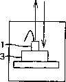
图19是以往光收发机的概略图。该光收发机具有信号传送用发光器件1及受光器件3。发光器件1及受光器件3可安装于光透射性的单个外壳中。Fig. 19 is a schematic diagram of a conventional optical transceiver. This optical transceiver includes a light emitting device 1 for signal transmission and a light receiving device 3 . The light-emitting device 1 and the light-receiving device 3 can be mounted in a single light-transmitting case.

图20是以往其它光收发机的概略图。发光器件1配置于受光器件3之上。据此,该光收发机被小型化,而且发光器件1及受光器件3可以通过同一光纤进行收发。Fig. 20 is a schematic diagram of another conventional optical transceiver. The light emitting device 1 is arranged on the light receiving device 3 . Accordingly, the optical transceiver is downsized, and the light emitting device 1 and the light receiving device 3 can transmit and receive through the same optical fiber.

施加给受光器件2的反偏压越大,则受光器件2的电容和电阻有关高频信号变得越小。因而,该反偏压越大,光接收机越适于高速通信。The larger the reverse bias voltage applied to the light receiving device 2 is, the smaller the capacitance and resistance of the light receiving device 2 related to the high-frequency signal become. Therefore, the larger the reverse bias voltage is, the more suitable the optical receiver is for high-speed communication.

但是,在以往的光接收机中,将向放大电路所供给电源电压VCC以上的电压施加给受光器件2是不可能的。也就是说,存在光接收机的传送速度因电源电压的值而被限制这样的问题。However, in the conventional optical receiver, it is impossible to apply a voltage equal to or higher than the power supply voltage V CC supplied to the amplifier circuit to the light receiving device 2 . That is, there is a problem that the transmission speed of the optical receiver is limited by the value of the power supply voltage.

通过减小受光器件2的面积,而可以减小受光器件2的电容。但是,若减小受光器件2的面积,则存在下述问题所在,即来自受光器件2的光电流变小并且难以实现和传送光信号的光纤之间的结合。By reducing the area of the light receiving device 2, the capacitance of the light receiving device 2 can be reduced. However, if the area of the light receiving device 2 is reduced, there is a problem that the photocurrent from the light receiving device 2 becomes small and it is difficult to achieve coupling with an optical fiber that transmits an optical signal.

另外,在图19及图20所示的以往光收发机中,发光器件1通过由电源而产生的正偏压对光进行放射,受光器件3通过由电源而产生的反偏压将光信号变换成电信号。因而,发光器件1依赖于电源电压,不能接受超过电源电压的电压供给。另外,受光器件3也依赖于电源电压,不能接受超过电源电压的电压供给。据此,受光器件3可接收的光信号速度因电源电压而被限制。In addition, in the conventional optical transceiver shown in FIG. 19 and FIG. 20, the light-emitting device 1 emits light by the forward bias voltage generated by the power supply, and the light-receiving device 3 converts the optical signal by the reverse bias voltage generated by the power supply. into an electrical signal. Therefore, the light emitting device 1 depends on the power supply voltage, and cannot receive a voltage supply exceeding the power supply voltage. In addition, the light receiving device 3 also depends on the power supply voltage, and cannot receive a voltage supply exceeding the power supply voltage. Accordingly, the speed of the optical signal that can be received by the light receiving device 3 is limited by the power supply voltage.

作为与Related Background Art相关的文献,有特开平6-216738号公报及特开平4-113713号公报。Documents related to Related Background Art include JP-A-6-216738 and JP-A-4-113713.

发明内容Contents of the invention

采用按照本发明的实施方式得到的光接收机,具备:第1受光器件,用来将光信号向电信号进行变换并将该电信号从一端予以输出;受光器件列,由多个第2受光器件构成,该第2受光器件与上述第1受光器件的另一端连接以向上述第1受光器件供给电力,并且相互串联连接。The optical receiver obtained according to the embodiment of the present invention is provided with: a first light receiving device for converting an optical signal into an electrical signal and outputting the electrical signal from one end; a row of light receiving devices consisting of a plurality of second light receiving devices The device configuration is that the second light receiving device is connected to the other end of the first light receiving device to supply power to the first light receiving device, and is connected in series to each other.

采用按照本发明的实施方式得到的光发送机,具备:表面发光型发光器件,用来将电信号变换成光信号对该光信号进行发送;受光器件列,由多个受光器件构成,该受光器件用来从上述发光器件接受光的照射以产生电力并且相互串联连接,其特征为,从上述发光器件上面所放射的光作为光信号加以使用,从上述发光器件内面所放射的光照射到上述受光器件列。The optical transmitter obtained according to the embodiment of the present invention is equipped with: a surface-emitting light-emitting device for converting an electrical signal into an optical signal to transmit the optical signal; a light-receiving device row consisting of a plurality of light-receiving devices, The device is used to receive light irradiation from the above-mentioned light-emitting device to generate power and is connected in series with each other. It is characterized in that the light emitted from the above-mentioned light-emitting device is used as an optical signal, and the light emitted from the inner surface of the above-mentioned light-emitting device is irradiated to the above-mentioned Receiver column.

采用按照本发明的实施方式得到的光收发机,具备:发光器件,用来将电信号变换成光信号并发送该光信号;第1受光器件,用来接收上述光信号将其变换成电信号并对该电信号予以输出;受光器件列,由多个第2受光器件构成,该第2受光器件用来从上述发光器件接受光的照射向上述第1受光器件供给电力,并且串联连接于上述发光器件和上述第1受光器件之间。The optical transceiver obtained according to the embodiment of the present invention is provided with: a light-emitting device for converting an electrical signal into an optical signal and transmitting the optical signal; a first light-receiving device for receiving the above-mentioned optical signal and converting it into an electrical signal and output the electrical signal; the light-receiving device column is composed of a plurality of second light-receiving devices, and the second light-receiving device is used to receive light irradiation from the above-mentioned light-emitting device to supply power to the above-mentioned first light-receiving device, and is connected in series to the above-mentioned Between the light-emitting device and the above-mentioned first light-receiving device.

附图说明Description of drawings

图1A是按照本发明所涉及第1实施方式的光接收机电路图。FIG. 1A is a circuit diagram of an optical receiver according to a first embodiment of the present invention.

图1B是按照本发明所涉及第2实施方式的光接收机电路图。Fig. 1B is a circuit diagram of an optical receiver according to a second embodiment of the present invention.

图2是作为光接收机100的第1变形例表示光接收机100a的概略图。FIG. 2 is a schematic diagram showing an optical receiver 100 a as a first modification of the optical receiver 100 .

图3是作为光接收机100的第2变形例表示光接收机100b的概略图。FIG. 3 is a schematic diagram showing an optical receiver 100 b as a second modification of the optical receiver 100 .

图4是按照本发明所涉及第3实施方式的光接收机200的电路图。FIG. 4 is a circuit diagram of an optical receiver 200 according to a third embodiment of the present invention.

图5是以往光接收机的电路图。Fig. 5 is a circuit diagram of a conventional optical receiver.

图6是按照本发明所涉及第4实施方式的光发送机300的剖面图。Fig. 6 is a cross-sectional view of an optical transmitter 300 according to a fourth embodiment of the present invention.

图7是发光器件130的平面图。FIG. 7 is a plan view of the light emitting device 130 .

图8是发光器件130的底面图。FIG. 8 is a bottom view of the light emitting device 130 .

图9是光发送机300的等效电路图。FIG. 9 is an equivalent circuit diagram of the optical transmitter 300 .

图10是光发送机300的等效电路图。FIG. 10 is an equivalent circuit diagram of the optical transmitter 300 .

图11是按照本发明所涉及第5实施方式的光发送机400的剖面图。Fig. 11 is a cross-sectional view of an optical transmitter 400 according to a fifth embodiment of the present invention.

图12是光发送机400中光发送芯片130的平面图。FIG. 12 is a plan view of the optical transmission chip 130 in the optical transmitter 400 .

图13是光发送机400中光发送芯片130的底面图。FIG. 13 is a bottom view of the optical transmission chip 130 in the optical transmitter 400 .

图14是按照本发明所涉及第6实施方式的光收发机500的剖面图。Fig. 14 is a cross-sectional view of an optical transceiver 500 according to a sixth embodiment of the present invention.

图15是按照本发明所涉及第7实施方式的光收发机600的剖面图。Fig. 15 is a cross-sectional view of an optical transceiver 600 according to a seventh embodiment of the present invention.

图16是图14或图15所示的光收发机500或600的等效电路图。FIG. 16 is an equivalent circuit diagram of the optical transceiver 500 or 600 shown in FIG. 14 or 15 .

图17是图14或图15所示的光收发机500或600的等效电路图。FIG. 17 is an equivalent circuit diagram of the optical transceiver 500 or 600 shown in FIG. 14 or 15 .

图18是按照本发明所涉及第8实施方式的光发送机700的剖面图。Fig. 18 is a cross-sectional view of an optical transmitter 700 according to an eighth embodiment of the present invention.

图19是以往光收发机的概略图。Fig. 19 is a schematic diagram of a conventional optical transceiver.

图20是以往光收发机的概略图。Fig. 20 is a schematic diagram of a conventional optical transceiver.

具体实施方式Detailed ways

下面,参照附图对根据本发明的实施方式予以说明。这些实施方式并不是限定本发明的方式。Hereinafter, embodiments according to the present invention will be described with reference to the drawings. These embodiments do not limit the present invention.

首先,说明本发明所涉及光接收机的实施方式。本发明的光接收机的实施方式具备受光器件列,由相互串联连接的多个受光器件构成。受光器件列通过接受光的照射来产生比电源电压更大的光电压。通过将该光电压施加给受光器件,光接收机可以适应高速通信。First, an embodiment of an optical receiver according to the present invention will be described. An embodiment of the optical receiver of the present invention includes a light receiving device array, which is composed of a plurality of light receiving devices connected in series. The light-receiving device array generates a photovoltage higher than the power supply voltage by receiving light irradiation. By applying this photovoltage to the photoreceiving device, the photoreceiver can be adapted to high-speed communication.

(第1实施方式)(first embodiment)

图1(A)是按照本发明所涉及第1实施方式的光接收机100的电路图。光接收机100具备受光器件9、受光器件20及放大电路40。受光器件9具有多个且相互串联连接,用来接受光P来产生电力。此处,将相互串联连接的多个受光器件9称为受光器件列10。受光器件列10的阴极侧与地面连接,其阳极侧与受光器件20的阴极连接。受光器件20的阳极与放大电路40的输入端连接。受光器件20从光纤(未图示)接收光信号S,将该光信号S向光电流(下面,也称为电信号)进行变换。放大电路40用来从电源VCC接受电力供给,借此对从受光器件20所输出的电信号进行放大。再者,放大电路40将放大后的电信号从输出端OUT予以输出。FIG. 1(A) is a circuit diagram of an optical receiver 100 according to a first embodiment of the present invention. The optical receiver 100 includes a light receiving device 9 , a light receiving device 20 , and an amplifier circuit 40 . A plurality of light receiving devices 9 are connected in series to receive light P to generate electric power. Here, the plurality of light receiving devices 9 connected in series are referred to as a light receiving device row 10 . The cathode side of the photoreceiving device array 10 is connected to the ground, and the anode side thereof is connected to the cathode of the photoreceiving device 20 . The anode of the light receiving device 20 is connected to the input end of the amplifier circuit 40 . The light receiving device 20 receives an optical signal S from an optical fiber (not shown), and converts the optical signal S into a photocurrent (hereinafter also referred to as an electrical signal). The amplification circuit 40 is used to receive power supply from the power supply V CC , thereby amplifying the electric signal output from the light receiving device 20 . Furthermore, the amplifying circuit 40 outputs the amplified electrical signal from the output terminal OUT.

(第2实施方式)(second embodiment)

图1(B)表示按照本发明所涉及第2实施方式的光接收机101。光接收机101与光接收机100的不同之处是,受光器件列10的阳极侧与地面GND连接,其阴极侧与受光器件20连接。另外,光接收机101与光接收机100的不同之处为,受光器件20的阳极侧与受光器件列10连接,其阴极侧与放大电路40的输入端连接。FIG. 1(B) shows an optical receiver 101 according to a second embodiment of the present invention. The difference between the optical receiver 101 and the optical receiver 100 is that the anode side of the light receiving device array 10 is connected to the ground GND, and the cathode side thereof is connected to the light receiving device 20 . In addition, the difference between the optical receiver 101 and the optical receiver 100 is that the anode side of the light receiving device 20 is connected to the light receiving device column 10 , and the cathode side is connected to the input end of the amplifier circuit 40 .

受光器件9及受光器件20例如是光电二极管等。虽然多个受光器件9也可以具有各自不同的特性,但是最好多个受光器件9具有相互相同的特性。借此,该受光器件列10所产生的电力能够根据串联连接的受光器件9的个数进行控制。另外,由于多个受光器件9具有相互相同的特性,因而光接收机100的制造变得较为容易。此处所说受光器件的特性指的是,器件尺寸、从光信号向光电流或光电压的变换效率以及寄生电容等。The light receiving device 9 and the light receiving device 20 are, for example, photodiodes or the like. Although the plurality of light receiving devices 9 may have different characteristics, it is preferable that the plurality of light receiving devices 9 have the same characteristics as each other. Thereby, the electric power generated by the light receiving device array 10 can be controlled according to the number of light receiving devices 9 connected in series. In addition, since the plurality of light receiving devices 9 have the same characteristics as each other, the manufacture of the optical receiver 100 becomes easier. The characteristics of the light-receiving device mentioned here refer to device size, conversion efficiency from optical signal to photocurrent or photovoltage, parasitic capacitance, and the like.

在光接收机100能够容易制造这样的观点上,受光器件9的特性也可以与受光器件20的相同。但是,受光器件9的特性也可以使之与受光器件20的不同。例如,在将相同的反偏压施加给受光器件9及20的场合下,受光器件9的有关高频信号的电容及电阻可以比受光器件20的更大。借此,如同图3所示的方式那样,在向受光器件9及20双方照射出光信号S的场合下,受光器件20可以将光信号S作为信号进行接收,另一方面受光器件9可以将光信号S作为连续的光而不断产生电力。The characteristics of the light receiving device 9 may be the same as those of the light receiving device 20 from the viewpoint that the optical receiver 100 can be easily manufactured. However, the characteristics of the light receiving device 9 may be different from those of the light receiving device 20 . For example, when the same reverse bias voltage is applied to the light receiving devices 9 and 20, the capacitance and resistance of the light receiving device 9 with respect to high-frequency signals may be larger than those of the light receiving device 20. Thereby, like the mode shown in FIG. 3, when the light signal S is emitted to both the light receiving devices 9 and 20, the light receiving device 20 can receive the light signal S as a signal, and the light receiving device 9 can receive the light signal S as a signal. The signal S continuously generates electricity as a continuous light.

根据第1及第2实施方式,按照向受光器件列10所照射的光P的强度来调节受光器件9的个数。借此,受光器件列10的输出电压能够变得比电源电压VCC更大。由于受光器件列10的输出电压超过电源电压VCC,因而施加给受光器件20的反偏压超过电源电压VCC,因此受光器件20有关高频信号的电容和电阻变得比以往技术的更小。据此,光接收机100无需依赖于电源电压VCC,就可以适应高速通信。According to the first and second embodiments, the number of light receiving devices 9 is adjusted according to the intensity of the light P irradiated to the photo receiving device row 10 . Thereby, the output voltage of the photodetector array 10 can become larger than power supply voltage V CC . Since the output voltage of the light-receiving device column 10 exceeds the power supply voltage V CC , the reverse bias voltage applied to the light-receiving device 20 exceeds the power supply voltage V CC , so the capacitance and resistance of the light-receiving device 20 related to high-frequency signals become smaller than in the prior art . Accordingly, the optical receiver 100 can adapt to high-speed communication without depending on the power supply voltage V CC .

图2是作为光接收机100的第1变形例表示光接收机100a的概略图。在光接收机100a中,受光器件列10和受光器件20分别作为独立的装置来构成。受光器件列10与发光器件30一起形成电动势装置50。发光器件30用来从外部接受电力供给,借此放射出光。受光器件列10用来接受来自发光器件30的光照射以产生电力。发光器件30例如是LED和激光二极管等。发光器件30也可以从电源电压VCC接受电力供给。发光器件30没有必要是发送用装置。FIG. 2 is a schematic diagram showing an optical receiver 100 a as a first modification of the optical receiver 100 . In the optical receiver 100a, the light receiving device array 10 and the light receiving device 20 are constituted as independent devices, respectively. The light receiving device array 10 forms an electromotive force device 50 together with the light emitting device 30 . The light emitting device 30 is used to receive power supply from the outside, thereby emitting light. The light-receiving device array 10 is used to receive light irradiation from the light-emitting device 30 to generate electricity. The light emitting device 30 is, for example, an LED, a laser diode, or the like. The light emitting device 30 can also receive power supply from the power supply voltage V CC . The light emitting device 30 is not necessarily a device for transmission.

受光器件20与放大电路40一起形成接收装置60。The light receiving device 20 forms a receiving device 60 together with the amplifier circuit 40 .

光接收机100a具有与光接收机100相同的效果。再者,根据本方式,由于受光器件列10和受光器件20各自独立,因而受光器件列10可以与光信号S无关,来产生电力。The optical receiver 100 a has the same effects as the optical receiver 100 . Furthermore, according to this aspect, since the light receiving device array 10 and the light receiving device 20 are independent, the light receiving device array 10 can generate electric power regardless of the optical signal S.

图3是作为光接收机100的第2变形例表示光接收机100b的概略图。光接收机100b与光接收机100a的不同之处是,受光器件列10和受光器件20被集成化到同一个芯片上。因而,受光器件列10与受光器件20一起接受光信号S的照射,借此产生电力。在图3所示的光接收机100b中,受光器件列10配置于光信号S照射最强的光接收机100b的中心部分,并且受光器件20配置于其外围部分。据此,受光器件列10可以向受光器件20供给足够大的电力。另一方面,为了受光器件20正确接收信号,也可以将受光器件20配置于光接收机100b的中心部分,将受光器件列10配置于其外围部分。FIG. 3 is a schematic diagram showing an optical receiver 100 b as a second modification of the optical receiver 100 . The difference between the optical receiver 100b and the optical receiver 100a is that the light receiving device array 10 and the light receiving device 20 are integrated on the same chip. Therefore, the light receiving device array 10 receives the irradiation of the light signal S together with the light receiving device 20 , thereby generating electric power. In the optical receiver 100b shown in FIG. 3, the light receiving device array 10 is arranged in the central part of the optical receiver 100b where the light signal S is irradiated the strongest, and the light receiving device 20 is arranged in the peripheral part thereof. Accordingly, the photoreceiving device array 10 can supply sufficient electric power to the photoreceiving device 20 . On the other hand, in order for the light receiving device 20 to correctly receive a signal, the light receiving device 20 may be arranged in the central part of the optical receiver 100b, and the light receiving device array 10 may be arranged in the peripheral part thereof.

光接收机100b具有与光接收机100相同的效果。再者,根据本方式,由于受光器件列10通过光信号S产生电力,因而不需要受光器件列10专用的发光器件。另外,由于受光器件列10及受光器件20作为同一个芯片来构成,因而本方式能够比光接收机100a更加小型化。The optical receiver 100b has the same effects as the optical receiver 100 . Furthermore, according to this aspect, since the light receiving device array 10 generates electric power from the optical signal S, there is no need for a dedicated light emitting device for the light receiving device array 10 . In addition, since the light-receiving device array 10 and the light-receiving device 20 are configured as the same chip, this embodiment can be further downsized than the optical receiver 100a.

光接收机100b还在形成受光器件列10及受光器件20的芯片上进一步装入放大电路40。借此,光接收机100b能够进一步被小型化。In the optical receiver 100 b, an amplifier circuit 40 is further incorporated on the chip forming the light receiving device array 10 and the light receiving device 20 . Thereby, the optical receiver 100b can be further miniaturized.

(第3实施方式)(third embodiment)

图4是按照本发明所涉及第3实施方式的光接收机200的电路图。光接收机200与第1实施方式的不同之处是进一步具备电容器70,该电容器与受光器件列10并联连接。电容器70在来自受光器件列10的电力暂时产生变化时,可以补偿该电力变化。例如,在光P的照射强度暂时变弱的场合下,电容器70可以取代受光器件列10而向受光器件20以某种程度供给电荷。在光P的照射强度暂时变强的场合下,电容器70可以取代受光器件列10以某种程度储存该电荷。换言之,电容器70可以使从受光器件列10向受光器件20的产生于电力中的噪声平滑。为了使该电力更为稳定,可以进一步加大电容器70的电容。FIG. 4 is a circuit diagram of an optical receiver 200 according to a third embodiment of the present invention. The optical receiver 200 differs from the first embodiment in that it further includes a capacitor 70 connected in parallel to the photoreceiving device array 10 . The capacitor 70 can compensate for the power change when the power from the photoreceiving device array 10 temporarily changes. For example, when the irradiation intensity of the light P is temporarily weakened, the capacitor 70 may supply a certain amount of charge to the light receiving device 20 instead of the light receiving device row 10 . When the irradiation intensity of the light P becomes stronger temporarily, the capacitor 70 can store the electric charge to some extent instead of the light receiving device array 10 . In other words, the capacitor 70 can smooth noise generated in electric power from the light receiving device array 10 to the light receiving device 20 . In order to make the electric power more stable, the capacitance of the capacitor 70 can be further increased.

在图4中虽然受光器件列10通过光P产生电力,但是受光器件列10也可以通过光信号S产生电力。这种场合下,因为光信号S由高电压(高)及低电压(低)构成,所以受光器件列10所产生的电力通常不稳定。但是,因为电容器70使从受光器件列10所产生的光电动势平滑,所以给受光器件20供给大致一定的电压。In FIG. 4 , although the light receiving device array 10 generates power from the light P, the light receiving device row 10 may generate power from the light signal S. As shown in FIG. In this case, since the optical signal S consists of a high voltage (high) and a low voltage (low), the power generated by the light receiving device array 10 is usually unstable. However, since the capacitor 70 smoothes the photoelectromotive force generated from the photoreceiving device array 10 , a substantially constant voltage is supplied to the photoreceiving device 20 .

再者,本实施方式可以获得与第1实施方式相同的效果。电容器70也可以作为与受光器件列10及受光器件20不同的装置来构成。另外,电容器70为了小型化,也可以作为与受光器件列10或受光器件20的任一个相同的装置来构成。再者,电容器70也可以作为与受光器件列10及受光器件20相同的装置来构成。借此,光接收机20被进一步小型化。再者,电容器70也可以作为与受光器件列10、受光器件20及放大电路40相同的装置来构成。借此,光接收机200被进一步小型化。Furthermore, this embodiment can obtain the same effect as that of the first embodiment. The capacitor 70 may be configured as a device different from the photoreceiving device array 10 and the photoreceiving device 20 . In addition, the capacitor 70 may be configured as the same device as either the photoreceiving device array 10 or the photoreceiving device 20 for downsizing. In addition, the capacitor 70 may be configured as the same device as the photoreceiving device array 10 and the photoreceiving device 20 . Thereby, the optical receiver 20 is further miniaturized. In addition, the capacitor 70 may be configured as the same device as the photoreceiving device array 10 , the photoreceiving device 20 , and the amplifier circuit 40 . Thereby, the optical receiver 200 is further miniaturized.

还有,在图2到图4所示的实施方式中,受光器件列10及受光器件20各自的连接关系与图1(A)所示光接收机100的相同。但是,图2到图4所示实施方式的受光器件列10及受光器件20各自的连接关系,也可以与图1(B)所示光接收机101的相同。也就是说,在图2到图4所示的实施方式中,受光器件列10及受光器件20的方向也可以分别是反方向。在这种场合下,图2到图4所示的实施方式也具有各自的效果。In addition, in the embodiment shown in FIG. 2 to FIG. 4 , the connection relationship between the light receiving device array 10 and the light receiving device 20 is the same as that of the optical receiver 100 shown in FIG. 1(A) . However, the respective connection relationships of the light receiving device array 10 and the light receiving device 20 in the embodiments shown in FIGS. 2 to 4 may be the same as those of the optical receiver 101 shown in FIG. 1(B). That is to say, in the embodiments shown in FIGS. 2 to 4 , the directions of the light receiving device rows 10 and the light receiving devices 20 may also be opposite directions. In this case, the embodiments shown in FIGS. 2 to 4 also have respective effects.

按照上述实施方式的光接收机不受电源电压的限制,可以适应高速通信。The optical receiver according to the above-described embodiments is not limited by the power supply voltage, and can be used for high-speed communication.

接着,说明本发明所涉及光发送机及光收发机的实施方式。本发明所涉及光收发机的实施方式,用来将表面发光型发光器件的上面光作为光信号予以使用并且将其内面光照射到受光器件列。据此,受光器件列可以产生比电源电压更大的电力。Next, embodiments of an optical transmitter and an optical transceiver according to the present invention will be described. An embodiment of the optical transceiver according to the present invention is to use the upper surface light of a surface emission type light emitting device as an optical signal and irradiate the inner surface light to a light receiving device array. According to this, the light receiving device array can generate electric power larger than the power supply voltage.

(第4实施方式)(fourth embodiment)

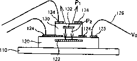
图6是按照本发明所涉及第4实施方式的光发送机300的剖面图。光发送机300具备引线框架110、受光芯片120及光发送芯片130。引线框架110由金属等导电性材料构成。在该引线框架110之上装配受光芯片120,在受光芯片120之上装配光发送芯片130。Fig. 6 is a cross-sectional view of an optical transmitter 300 according to a fourth embodiment of the present invention. The optical transmitter 300 includes a lead frame 110 , a light receiving chip 120 , and an optical transmitting chip 130 . The lead frame 110 is made of a conductive material such as metal. A light receiving chip 120 is mounted on the lead frame 110 , and a light sending chip 130 is mounted on the light receiving chip 120 .

在受光芯片120中形成有受光器件列122,由相互串联连接的多个受光器件构成。在光发送芯片130中形成有发光器件132,用来将电信号变换成光信号。受光器件例如是光电二极管。这种场合下,受光器件列122成为光电二极管·阵列。发光器件132是表面发光型发光器件,例如是LED或VCSEL(Vertical Cavity Surface-Emitting Laser)等。A light-receiving device column 122 is formed in the light-receiving chip 120 and is composed of a plurality of light-receiving devices connected in series. A light emitting device 132 is formed in the optical sending chip 130 for converting electrical signals into optical signals. The light receiving device is, for example, a photodiode. In this case, the photodetector array 122 becomes a photodiode array. The light emitting device 132 is a surface emitting light emitting device, such as an LED or a VCSEL (Vertical Cavity Surface-Emitting Laser).

处于受光器件列122和发光器件132之间的材料对光是透明(透光性)的,以使来自发光器件132的光直至受光器件列122都可透过。The material between the light-receiving device row 122 and the light-emitting device 132 is transparent (light-transmitting) to light, so that the light from the light-emitting device 132 can pass through to the light-receiving device row 122 .

光发送机300进一步具备电极124、125及134。电极124设置于受光芯片120和光发送芯片130之间,与发光器件132的任一方电极连接。电极134设置于光发送芯片130上,与发光器件132任另一方的电极连接。电极124例如与地面等基准电位连接,电极134例如连接到放大电路(未图示),该放大电路用来对发送用的电信号进行放大。电极125设置于受光芯片120上,与受光器件列122任一方的电极连接。再者,引线框架110与受光器件列122任另一方的电极连接。另外,引线框架110与地面等基准电位连接。The optical transmitter 300 further includes electrodes 124 , 125 and 134 . The electrode 124 is disposed between the light receiving chip 120 and the light sending chip 130 , and is connected to any electrode of the light emitting device 132 . The electrode 134 is provided on the light-transmitting chip 130 and connected to any other electrode of the light-emitting device 132 . The electrode 124 is connected to a reference potential such as ground, for example, and the electrode 134 is connected to an amplifier circuit (not shown) for amplifying an electrical signal for transmission, for example. The electrode 125 is disposed on the light receiving chip 120 and connected to any electrode of the light receiving device row 122 . Furthermore, the lead frame 110 is connected to the other electrode of the photodetector array 122 . In addition, the lead frame 110 is connected to a reference potential such as ground.

图7及图8分别是发光器件130的平面图及底面图。图7所示的电极134遮盖住开口部136以外的发光器件130表面。开口部136是为了使来自发光器件132的上面光P1通过而设置的。图8所示的电极124设置于发光器件130内面上的左右两侧。处于电极124间的光透过部28是为了使来自发光器件132的内面光P2向受光器件列122通过而设置的。7 and 8 are a plan view and a bottom view of the light emitting device 130, respectively. The electrode 134 shown in FIG. 7 covers the surface of the light emitting device 130 other than the opening 136 . The opening 136 is provided for passing the upper surface light P1 from the light emitting device 132 . The electrodes 124 shown in FIG. 8 are disposed on the left and right sides of the inner surface of the light emitting device 130 . The light transmitting portion 28 between the electrodes 124 is provided to allow the inner surface light P 2 from the light emitting device 132 to pass to the light receiving device array 122 .

下面,说明光发送机300的动作。Next, the operation of the optical transmitter 300 will be described.

若向电极134输入电信号,则在电极124和电极134之间产生电位差。借助于该电位差,正偏压被施加给发光器件132。由于发光器件132是表面发光型,因而发光器件132通过该正偏压从其上面及内面放射出光。从发光器件132上面所放射的上面光P1,经由空间或光纤(未图示)等的媒体,作为光信号发送给对方一侧的受光器件。另一方面,从发光器件132内面所放射的内面光P2照射到受光器件列122。When an electrical signal is input to electrode 134 , a potential difference is generated between electrode 124 and electrode 134 . By means of this potential difference, a forward bias voltage is applied to the light emitting device 132 . Since the light emitting device 132 is a surface emitting type, the light emitting device 132 emits light from the upper surface and the inner surface thereof by the positive bias voltage. The upper surface light P 1 radiated from the upper surface of the light emitting device 132 is sent as an optical signal to the other side's light receiving device through a medium such as space or an optical fiber (not shown). On the other hand, the inner surface light P2 radiated from the inner surface of the light emitting device 132 is irradiated to the light receiving device row 122 .

若光照射到受光器件列122上,则受光器件列122在其阳极和阴极之间产生电位差。根据本实施方式,由于引线框架110与地面连接,因而受光器件列122所产生的电位差从电极125作为输出电压VO被输出。When light is irradiated onto the photoreceiving device array 122, the photoreceiving device array 122 generates a potential difference between its anode and cathode. According to the present embodiment, since the lead frame 110 is connected to the ground, the potential difference generated in the photodetector array 122 is output from the electrode 125 as the output voltage V O.

在从发光器件132所发送的信号速度比较慢的场合下,受光器件列122的输出电压VO依赖于其信号速度。但是,在其信号速度比较快的场合下,输出电压VO大致成为直流电压。原因是,一般情况下受光器件列在其内部具有电容。When the signal speed transmitted from the light emitting device 132 is relatively slow, the output voltage V O of the light receiving device array 122 depends on the signal speed. However, when the signal speed is relatively fast, the output voltage V O becomes approximately a DC voltage. The reason is that, generally, the light-receiving device array has capacitance inside it.

在信号速度比较慢的场合下,为了从受光器件列122获得接近直流且稳定的输出电压VO,如图9及图10所示可以对受光器件列122并联连接电容器140。When the signal speed is relatively slow, in order to obtain a nearly DC and stable output voltage V O from the photodetector array 122, a capacitor 140 may be connected in parallel to the photodetector array 122 as shown in FIGS. 9 and 10 .

另外,一般来说发光器件即使在未实行信号发送的场合下,也发送出空闲信号等假信号或者低速的开/关信号。据此,即使是没有实行发送的待机时,受光器件列122也可以将输出电压VO输出。该输出电压VO的用途没有做出特别限定。例如,输出电压VO如下所述,可以用来向接收光信号的受光器件提供反偏压。In addition, in general, even when a light emitting device is not transmitting a signal, it transmits a glitch such as an idle signal or a low-speed ON/OFF signal. According to this, even in the standby time when transmission is not performed, the light-receiving element array 122 can output the output voltage V O. The application of the output voltage V O is not particularly limited. For example, the output voltage V O , as described below, can be used to provide a reverse bias voltage to the light-receiving device receiving the light signal.

输出电压VO依赖于受光器件123的个数,该受光器件在受光器件列122中相互串联连接。因而,为了将输出电压VO比电源电压进一步加大,而可以调节受光器件123的个数。受光器件123例如是光电二极管。虽然多个受光器件123也可以具有各自不同的特性,但是最好多个受光器件123具有相互相同的特性。借此,该受光器件列122所产生的电力能够借助于串联连接的受光器件123个数轻易地进行控制。另外,由于多个受光器件123具有相互相同的特性,因而光接收机300的制造变得较为容易。此处所说受光器件的特性指的是,器件尺寸、从光信号向光电流、光电压的变换效率以及寄生电容等。The output voltage V O depends on the number of light receiving devices 123 connected in series in the light receiving device column 122 . Therefore, the number of light receiving devices 123 can be adjusted in order to further increase the output voltage V O from the power supply voltage. The light receiving device 123 is, for example, a photodiode. Although the plurality of light receiving devices 123 may have different characteristics, it is preferable that the plurality of light receiving devices 123 have the same characteristics. Thereby, the power generated by the light receiving device array 122 can be easily controlled by the number of the light receiving devices 123 connected in series. In addition, since the plurality of light receiving devices 123 have the same characteristics as each other, the manufacture of the optical receiver 300 becomes easier. The characteristics of the light-receiving device mentioned here refer to device size, conversion efficiency from optical signal to photocurrent, photovoltage, and parasitic capacitance.

根据本实施方式的光发送机300,可以供给比从外部所供给的电源电压VCC(参见图16)大的电压。另外,光发送机发光器件132的上面光P1作为光信号使用于通信,其内面光P2使用于电力供给。也就是说,发光器件132同时使用于信号传送及电极供给。据此,光发送机300较为能够被小型化。According to the optical transmitter 300 of this embodiment, a voltage higher than the power supply voltage VCC (see FIG. 16 ) supplied from the outside can be supplied. In addition, the upper surface light P1 of the light emitting device 132 of the optical transmitter is used for communication as an optical signal, and the inner surface light P2 is used for power supply. That is, the light emitting device 132 is used for both signal transmission and electrode supply. Accordingly, the optical transmitter 300 can be reduced in size relatively.

图9及图10是光发送机300的等效电路图。在图9所示的电路图中,发光器件132按照从阳极所输出的发送用电信号S0放射出光。受光器件列122接受来自发光器件132的内面光P2的照射,借此从阳极将输出电压VO输出。受光器件列122及发光器件132各自的阴极共同与地面连接。9 and 10 are equivalent circuit diagrams of the optical transmitter 300 . In the circuit diagram shown in FIG. 9, the light emitting device 132 emits light in accordance with the transmission electrical signal S0 output from the anode. The light-receiving device row 122 is irradiated with the inner surface light P2 from the light-emitting device 132, thereby outputting the output voltage V O from the anode. The respective cathodes of the light-receiving device array 122 and the light-emitting device 132 are commonly connected to the ground.

在本实施方式中,电容器140对受光器件列122并联连接。电容器140例如连接于图6所示的电极124和引线框架110之间。电容器140也可以设置于光发送机300的外部。另外,电容器140也可以是受光芯片120内的寄生电容。通过电容器140,使输出电压VO平滑,光发送机300可以输出稳定的输出电压VOIn the present embodiment, the capacitor 140 is connected in parallel to the light receiving device array 122 . The capacitor 140 is connected, for example, between the electrode 124 shown in FIG. 6 and the lead frame 110 . The capacitor 140 may also be provided outside the optical transmitter 300 . In addition, the capacitor 140 may be a parasitic capacitance in the light receiving chip 120 . Through the capacitor 140, the output voltage V O is smoothed, and the optical transmitter 300 can output a stable output voltage V O .

在图10所示的电路图中,与图9所示的电路图的不同之处是受光器件列122的阳极与地面连接,从其阴极将输出电压VO输出。其它结构与图10所示的电路相同。即便是图9及图10所示的任一电路结构,都不损失光发送机300的效果。In the circuit diagram shown in FIG. 10 , the difference from the circuit diagram shown in FIG. 9 is that the anodes of the light receiving device array 122 are connected to the ground, and the output voltage V O is output from the cathodes thereof. Other structures are the same as the circuit shown in FIG. 10 . The effects of the optical transmitter 300 are not lost even in any of the circuit configurations shown in FIGS. 9 and 10 .

(第5实施方式)(fifth embodiment)

图11是按照本发明所涉及第5实施方式的光发送机400的剖面图。光发送机400与第4实施方式的不同之处是,电极124设置于光发送芯片130的上面。Fig. 11 is a cross-sectional view of an optical transmitter 400 according to a fifth embodiment of the present invention. The difference between the optical transmitter 400 and the fourth embodiment is that the electrodes 124 are provided on the upper surface of the optical transmitter chip 130 .

图12及图13是光发送机400中光发送芯片130的平面图及底面图。如图12所示,表示在光发送芯片130的上面,在开口部136的两侧设置电极124及134的状态。另外,如图13所示在光发送芯片130的底面未设置电极。12 and 13 are plan views and bottom views of the optical transmitting chip 130 in the optical transmitter 400 . As shown in FIG. 12 , a state in which electrodes 124 and 134 are provided on both sides of an opening 136 is shown on the upper surface of the optical transmission chip 130 . In addition, no electrodes are provided on the bottom surface of the light transmitting chip 130 as shown in FIG. 13 .

光发送机400与第4实施方式有所不同,在光发送芯片130和受光芯片120之间不具有电极。因而,根据本实施方式,不出现电极遮盖内面光P2的状况。另外,本实施方式与第1实施方式相比制造更为容易。再者,本实施方式具有与第4实施方式相同的效果。The optical transmitter 400 differs from the fourth embodiment in that it does not have electrodes between the optical transmitting chip 130 and the light receiving chip 120 . Therefore, according to the present embodiment, there is no situation in which the electrodes cover the inner surface light P2 . In addition, this embodiment is easier to manufacture than the first embodiment. In addition, this embodiment has the same effect as 4th Embodiment.

(第6实施方式)(sixth embodiment)

图14是按照本发明所涉及第6实施方式的光收发机500的剖面图。本实施方式与第4及第5实施方式的不同之处是,不只是光发送机还具备有光接收机。换言之,也可以认为本实施方式是将采用第4或第5实施方式的光发送机应用于光接收机中的实施方式。Fig. 14 is a cross-sectional view of an optical transceiver 500 according to a sixth embodiment of the present invention. This embodiment differs from the fourth and fifth embodiments in that not only an optical transmitter but also an optical receiver is provided. In other words, this embodiment can also be considered as an embodiment in which the optical transmitter according to the fourth or fifth embodiment is applied to an optical receiver.

光发送机301也可以是图6所示的光发送机300或图11所示的光发送机400的任一个。从光发送机301所输出的电压VO被施加给光接收机302。The optical transmitter 301 may be either the optical transmitter 300 shown in FIG. 6 or the optical transmitter 400 shown in FIG. 11 . The voltage V O output from the optical transmitter 301 is applied to the optical receiver 302 .

光接收机302具备引线框架310及光接收芯片320。引线框架310最好由下述材料构成,即与引线框架110相同的材料。光接收芯片320具备受光器件322。受光器件322例如是光电二极管,用来接收光信号P3将其变换成电信号,经由引线330将该电信号输出。The optical receiver 302 includes a lead frame 310 and an optical receiving chip 320 . Lead frame 310 is preferably constructed of the same material as lead frame 110 . The light receiving chip 320 includes a light receiving device 322 . The light receiving device 322 is, for example, a photodiode, which is used to receive the light signal P 3 and transform it into an electrical signal, and output the electrical signal through the wire 330 .

引线框架310与受光器件322的阳极或阴极任一方的电极连接。引线330与受光器件322的阳极或阴极任另一方的电极连接。The lead frame 310 is connected to either an anode or a cathode electrode of the light receiving device 322 . The lead wire 330 is connected to either an anode electrode or a cathode electrode of the light receiving device 322 .

还有,受光器件列122相当于有关光接收机的第1到第3实施方式中的受光器件列10。受光器件322相当于第1到第3实施方式中的受光器件20。In addition, the light-receiving element array 122 corresponds to the light-receiving element array 10 in the first to third embodiments of the optical receiver. The light receiving device 322 corresponds to the light receiving device 20 in the first to third embodiments.

根据本实施方式,与光发送机301的电极125所连接的引线126与引线框架310连接。借此,光发送机301可以将输出电压VO向受光器件322进行供给。通过该输出电压VO,受光器件322可以接受反偏压,并将光信号P3向电信号进行变换。如上所述,输出电压VO能够成为比外部的电源电压VCC(参见图16)更大的电压。因而,受光器件322可以接受比外部电源电压VCC更大的偏压。据此,受光器件322与高频信号有关的电容及电阻变得比较小,受光器件322能够适应于高速通信。According to this embodiment, the lead wire 126 connected to the electrode 125 of the optical transmitter 301 is connected to the lead frame 310 . Thereby, the optical transmitter 301 can supply the output voltage V O to the light receiving device 322 . Through the output voltage V O , the light receiving device 322 can receive the reverse bias voltage and convert the optical signal P 3 into an electrical signal. As described above, the output voltage V O can be higher than the external power supply voltage V CC (see FIG. 16 ). Therefore, the light receiving device 322 can accept a bias voltage greater than the external power supply voltage V CC . Accordingly, the capacitance and resistance of the light receiving device 322 related to high-frequency signals are relatively small, and the light receiving device 322 can be adapted to high-speed communication.

(第7实施方式)(seventh embodiment)

图15是按照本发明所涉及第7实施方式的光收发机600的剖面图。本实施方式与第6实施方式的不同之处是,光发送机及光接收机被一体化。在本实施方式中,光发送芯片130及光接收芯片320装配于共用的受光芯片120上。受光芯片120装配于单个引线框架110上。这样,由于光收发机600安装于单个引线框架110上,因而构成光收发机600的部件件数变少。Fig. 15 is a cross-sectional view of an optical transceiver 600 according to a seventh embodiment of the present invention. This embodiment differs from the sixth embodiment in that an optical transmitter and an optical receiver are integrated. In this embodiment, the light transmitting chip 130 and the light receiving chip 320 are assembled on the common light receiving chip 120 . The light receiving chip 120 is mounted on a single lead frame 110 . In this way, since the optical transceiver 600 is mounted on a single lead frame 110, the number of parts constituting the optical transceiver 600 is reduced.

在第6实施方式中,受光器件322一方的电极与引线框架110连接。但是,在本实施方式中受光器件322一方的电极直接连接于电极125上,该电极用来将输出电压VO输出。据此,根据本实施方式,输出电压VO可以在不因引线126等的电阻而衰减的状况下,向受光器件322进行供给。另外,还不需要引线126。与此相伴,也不需要引线126的接续。本实施方式进一步具有与第6实施方式相同的效果。In the sixth embodiment, one electrode of the light receiving device 322 is connected to the lead frame 110 . However, in this embodiment, one electrode of the light receiving device 322 is directly connected to the electrode 125, and this electrode is used to output the output voltage V O. Accordingly, according to the present embodiment, the output voltage V O can be supplied to the light receiving device 322 without being attenuated by the resistance of the lead wire 126 or the like. Additionally, lead wires 126 are not required. Along with this, the connection of the lead wire 126 is also unnecessary. This embodiment further has the same effects as those of the sixth embodiment.

图16是图14或图15所示的光收发机500或600的等效电路图。虚线框C1内的电路相当于图9所示的电路。发光器件132的阳极与放大电路AMP1的输出端连接。发光器件132的阴极与地面连接。受光器件322的阳极与放大电路AMP2的输入端连接。受光器件列122的阳极与受光器件322的阴极连接。受光器件列122的阴极与地面连接。FIG. 16 is an equivalent circuit diagram of the optical transceiver 500 or 600 shown in FIG. 14 or 15 . The circuit inside the dotted frame C1 corresponds to the circuit shown in FIG. 9 . The anode of the light emitting device 132 is connected to the output terminal of the amplification circuit AMP1 . The cathode of the light emitting device 132 is connected to ground. The anode of the light receiving device 322 is connected to the input terminal of the amplifier circuit AMP 2 . The anodes of the light receiving device columns 122 are connected to the cathodes of the light receiving devices 322 . The cathodes of the light receiving device array 122 are connected to the ground.

发送用的信号S1在放大电路AMP1中被放大,作为图9所示的发送用信号S0向发光器件132进行供给。据此,发光器件132放射出光P1及P2。受光器件列122接受光P2,输出比外部电源电压VCC更大的输出电压VOThe signal S 1 for transmission is amplified in the amplifier circuit AMP 1 and supplied to the light emitting device 132 as the signal S 0 for transmission shown in FIG. 9 . Accordingly, the light emitting device 132 emits light P 1 and P 2 . The light receiving element array 122 receives the light P 2 and outputs an output voltage V O higher than the external power supply voltage V CC .

输出电压VO作为反偏压被施加在受光器件322。据此,受光器件322可以接收光信号P3,将其向电信号进行变换。该电信号在放大电路AMP2中被放大作为信号S2予以输出。还有,在图16所示的电路中输出电压V0对于地面是高的电压。The output voltage V O is applied to the light receiving device 322 as a reverse bias voltage. Accordingly, the light receiving device 322 can receive the optical signal P 3 and convert it into an electrical signal. This electrical signal is amplified in the amplifier circuit AMP2 and output as a signal S2 . Also, in the circuit shown in FIG. 16, the output voltage V0 is a high voltage with respect to the ground.

图17是图14或图15所示的光收发机500或600的等效电路图。虚线框C2内的电路相当于图10所示的电路。发光器件132的阳极与放大电路AMP1的输出端连接。发光器件132的阴极与地面连接。受光器件322的阴极与放大电路AMP2的输入端连接。受光器件列122的阳极与地面连接。受光器件列122的阴极与受光器件322的阳极连接。FIG. 17 is an equivalent circuit diagram of the optical transceiver 500 or 600 shown in FIG. 14 or 15 . The circuit inside the dotted frame C2 corresponds to the circuit shown in FIG. 10 . The anode of the light emitting device 132 is connected to the output terminal of the amplification circuit AMP1 . The cathode of the light emitting device 132 is connected to ground. The cathode of the light receiving device 322 is connected to the input end of the amplifier circuit AMP 2 . The anodes of the light receiving device array 122 are connected to the ground. The cathodes of the light receiving device columns 122 are connected to the anodes of the light receiving devices 322 .

发送用的信号S1在放大电路AMP1中被放大,作为图10所示的发送用信号S0向发光器件132进行供给。据此,发光器件132放射出光P1及P2。受光器件列122接受光P2,输出与外部电源电压VCC相比作为绝对值更大的输出电压VOThe signal S 1 for transmission is amplified in the amplifier circuit AMP 1 and supplied to the light emitting device 132 as the signal S 0 for transmission shown in FIG. 10 . Accordingly, the light emitting device 132 emits light P 1 and P 2 . The light receiving element array 122 receives the light P 2 and outputs an output voltage V O having a larger absolute value than the external power supply voltage V CC .

输出电压VO向受光器件322作为反偏压被施加。据此,受光器件322可以接收光信号P3,将其向电信号进行变换。该电信号在放大电路AMP2中被放大作为信号S2予以输出。The output voltage V O is applied to the light receiving device 322 as a reverse bias voltage. Accordingly, the light receiving device 322 can receive the optical signal P 3 and convert it into an electrical signal. This electrical signal is amplified in the amplifier circuit AMP2 and output as a signal S2 .

图17所示的电路与图16所示电路的不同之处是,输出电压VO对于地面成为低的电压。但是,由于地面与受光器件列122的阳极侧连接,因而给受光器件列122施加反偏压。而且,由于输出电压VO与外部电源电压VCC相比作为绝对值更大,因而图17所示的电路可以与图16所示的电路相同进行动作。The difference between the circuit shown in FIG. 17 and the circuit shown in FIG. 16 is that the output voltage V O becomes a low voltage with respect to the ground. However, since the ground is connected to the anode side of the photoreceiving device array 122 , a reverse bias is applied to the photoreceiving device array 122 . Furthermore, since the output voltage V O is larger in absolute value than the external power supply voltage V CC , the circuit shown in FIG. 17 can operate in the same manner as the circuit shown in FIG. 16 .

另外,在图17所示的电路中,下述偏压被施加给光电二极管322,该偏压是对放大电路AMP2的偏压电位和受光器件列122的输出电压VO进行加法运算后的偏压。也就是说,图17所示的电路可以将比图16所示电路大的偏压施加给光电二极管322。In addition, in the circuit shown in FIG. 17, the following bias voltage is applied to the photodiode 322. The bias voltage is obtained by adding the bias voltage potential of the amplifier circuit AMP 2 and the output voltage V O of the light receiving device column 122. the bias. That is, the circuit shown in FIG. 17 can apply a larger bias voltage to the photodiode 322 than the circuit shown in FIG. 16 .

再者,在图17所示的电路中,由于受光器件列122的阳极从地面电位向负极侧偏置,因而外部电源电压VCC的噪声和波动难以影响到受光器件列122的输出电压VOFurthermore, in the circuit shown in FIG. 17 , since the anode of the photoreceiving device column 122 is biased from the ground potential to the negative side, the noise and fluctuation of the external power supply voltage V CC hardly affect the output voltage V O of the photoreceiving device column 122. .

图16及图17所示的发光器件132、受光器件322、受光器件列122、电容器140、放大电路AMP1及放大电路AMP2最好内置于同一个外壳内。借此,光收发机300被小型化。另外,光收发机300内的线路长度变短,不需要无用的电力。The light emitting device 132, the light receiving device 322, the light receiving device row 122, the capacitor 140, the amplifier circuit AMP1 and the amplifier circuit AMP2 shown in Fig. 16 and Fig. 17 are preferably built in the same housing. Thereby, the optical transceiver 300 is miniaturized. In addition, the length of the line in the optical transceiver 300 is shortened, and wasteful power is not required.

(第8实施方式)(eighth embodiment)

图18是按照本发明所涉及第8实施方式的光发送机700的剖面图。受光芯片120及光发送芯片130按横向排列配置于同一个引线框架110上。受光芯片120及光发送芯片130由透明树脂150进行遮盖。Fig. 18 is a cross-sectional view of an optical transmitter 700 according to an eighth embodiment of the present invention. The light receiving chip 120 and the light sending chip 130 are arranged horizontally on the same lead frame 110 . The light receiving chip 120 and the light transmitting chip 130 are covered with a transparent resin 150 .

在透明树脂150表面区域内,来自发光器件132的上面光P1所通过的区域R1相对于上面光P1的行进方向大致垂直相交。据此,上面光P1之中的直线光不用在区域R1上进行反射,就可以通过透明树脂150。In the surface area of the transparent resin 150, the region R1 through which the upper light P1 from the light emitting device 132 passes is substantially perpendicular to the traveling direction of the upper light P1 . Accordingly, the straight light among the upper light P1 can pass through the transparent resin 150 without being reflected on the region R1 .

另一方面,在透明树脂150的表面区域之内,区域R1的外围区域R2成为镜面状态。而且,外围区域R2被制成形,以使来自发光器件132的光向受光器件122进行反射。借此,上面光P1之中直线光的外围光反射到区域R2向受光器件列122进行照射。这样,发光器件132的上面光P1不仅作为光信号加以使用,上面光P1的一部分还照射到受光器件列122上。本实施方式可以只使用发光器件132的上面光P1来发送光信号,而且可以使受光器件122产生电力。On the other hand, within the surface region of the transparent resin 150, the peripheral region R2 of the region R1 becomes a mirror state. Also, the peripheral region R 2 is shaped so that light from the light emitting device 132 is reflected toward the light receiving device 122 . Thereby, the peripheral light of the straight light among the upper surface light P1 is reflected to the region R2 to be irradiated to the light-receiving device row 122 . In this way, the upper surface light P1 of the light emitting device 132 is not only used as an optical signal, but part of the upper surface light P1 is also irradiated on the light receiving device array 122 . In this embodiment, only the upper surface light P1 of the light emitting device 132 can be used to send an optical signal, and the light receiving device 122 can generate electricity.

为了使区域R2变成镜面状态,也可以在透明树脂150的表面施以涂层。另外,也可以在光发送机700的外部设置反射物。In order to make the region R2 into a mirror state, a coating may be applied to the surface of the transparent resin 150 . In addition, a reflector may be provided outside the optical transmitter 700 .

按照本实施方式的光发送机可以供给比电源电压大的电压。另外,按照本实施方式的光收发机无需依赖于电源电压,就可以实行高速通信。The optical transmitter according to this embodiment can supply a voltage higher than the power supply voltage. In addition, the optical transceiver according to this embodiment can perform high-speed communication without depending on the power supply voltage.

Claims (23)

1.一种光接收机,其特征为:具备1. A kind of optical receiver, it is characterized in that: Possess 第1受光器件,用来将光信号向电信号进行变换并将该电信号从一端予以输出;The first light-receiving device is used to convert the optical signal into an electrical signal and output the electrical signal from one end; 受光器件列,由多个相互串联连接第2受光器件构成,该多个第2受光器件与上述第1受光器件的另一端连接,以向上述第1受光器件供给电力。The light-receiving element row is composed of a plurality of second light-receiving elements connected in series, and the plurality of second light-receiving elements are connected to the other end of the first light-receiving element to supply electric power to the first light-receiving element. 2.根据权利要求1记载的光接收机,其特征为:2. The optical receiver according to claim 1, characterized in that: 进一步具备further equipped 放大电路,与上述第1受光器件的另一端连接,用来对从上述第1受光器件所输出的电信号进行放大予以输出。An amplifier circuit is connected to the other end of the first light receiving device, and is used to amplify and output the electric signal output from the first light receiving device. 3.根据权利要求1记载的光接收机,其特征为:3. The optical receiver according to claim 1, characterized in that: 上述受光器件列将比电力源更高的电力供给上述第1受光器件,该电力源用来向上述放大电路供给电力。The light-receiving device array supplies the first light-receiving device with higher power than a power source for supplying power to the amplifier circuit. 4.根据权利要求1记载的光接收机,其特征为:4. The optical receiver according to claim 1, characterized in that: 进一步具备further equipped 发光部,用来向上述受光器件列照射光。The light emitting unit irradiates light to the array of light receiving devices. 5.根据权利要求4记载的光接收机,其特征为:5. The optical receiver according to claim 4, characterized in that: 上述发光部是发光二极管或激光二极管。The light emitting unit is a light emitting diode or a laser diode. 6.根据权利要求1记载的光接收机,其特征为:6. The optical receiver according to claim 1, characterized in that: 进一步具备further equipped 电容器,与上述受光器件列并联连接。The capacitor is connected in parallel with the above-mentioned light-receiving device column. 7.根据权利要求1记载的光接收机,其特征为:7. The optical receiver according to claim 1, characterized in that: 上述受光器件列及上述第1受光器件形成于同一个基板上,The array of light receiving devices and the first light receiving device are formed on the same substrate, 上述受光器件列用来接受上述第1受光器件所接收的光信号照射以产生电力。The light-receiving device row is used to receive the light signal received by the first light-receiving device to generate electricity. 8.根据权利要求2记载的光接收机,其特征为:8. The optical receiver according to claim 2, characterized in that: 上述受光器件列、上述第1受光器件及上述放大电路形成于同一个基板上,The array of light-receiving elements, the first light-receiving element, and the amplifier circuit are formed on the same substrate, 上述受光器件列用来接受上述第1受光器件所接收的光信号照射以产生电力。The light-receiving device row is used to receive the light signal received by the first light-receiving device to generate electricity. 9.一种光发送机,其特征为:具备9. An optical transmitter, characterized by: having 表面发光型发光器件,用来将电信号变换成光信号并发送该光信号;A surface-emitting light-emitting device for converting an electrical signal into an optical signal and transmitting the optical signal; 受光器件列,由多个相互串联连接的受光器件构成,该受光器件用来从上述发光器件接受光的照射以产生电力,The light-receiving device column is composed of a plurality of light-receiving devices connected in series, and the light-receiving device is used to receive light irradiation from the above-mentioned light-emitting device to generate electricity, 从上述发光器件上面所放射的光作为光信号加以使用,从上述发光器件内面所放射的光照射到上述受光器件列。The light emitted from the upper surface of the light emitting device is used as an optical signal, and the light emitted from the inner surface of the light emitting device is irradiated to the array of light receiving devices. 10.根据权利要求9记载的光发送机,其特征为:10. The optical transmitter according to claim 9, characterized in that: 进一步具备further equipped 镜面部,用来使从上述发光器件上面所放射的光的一部分反射到上述受光器件列。The mirror portion reflects part of the light emitted from the upper surface of the light-emitting device to the array of light-receiving devices. 11.根据权利要求9记载的光发送机,其特征为:11. The optical transmitter according to claim 9, characterized in that: 进一步具备further equipped 电容器,与上述受光器件列并联连接。The capacitor is connected in parallel with the above-mentioned light-receiving device column. 12.根据权利要求9记载的光发送机,其特征为:12. The optical transmitter according to claim 9, characterized in that: 进一步具备further equipped 安装基板,由导体构成;a mounting substrate consisting of a conductor; 受光芯片,装配于上述安装基板上,形成上述受光器件列;A light-receiving chip is assembled on the above-mentioned mounting substrate to form the above-mentioned light-receiving device row; 光发送芯片,装配于上述受光芯片上,形成上述发光器件。The light sending chip is assembled on the above light receiving chip to form the above light emitting device. 13.根据权利要求12记载的光发送机,其特征为:13. The optical transmitter according to claim 12, characterized in that: 进一步具备further equipped 第1电极,设置于上述光发送芯片上,与上述发光器件一方的电极连接;The first electrode is arranged on the above-mentioned light-transmitting chip and connected to one electrode of the above-mentioned light-emitting device; 第2电极,设置于上述受光芯片和上述光发送芯片之间,与上述发光器件另一方的电极连接;The second electrode is arranged between the above-mentioned light-receiving chip and the above-mentioned light-transmitting chip, and is connected to the other electrode of the above-mentioned light-emitting device; 第3电极,设置于上述受光芯片上,与上述受光器件一方的电极连接,The third electrode is arranged on the above-mentioned light-receiving chip, and is connected to one electrode of the above-mentioned light-receiving device, 上述安装基板与上述受光器件另一方的电极连接。The mounting substrate is connected to the other electrode of the light receiving device. 14.根据权利要求12记载的光发送机,其特征为:14. The optical transmitter according to claim 12, characterized in that: 进一步具备further equipped 第1电极,设置于上述光发送芯片上,与上述发光器件一方的电极连接;The first electrode is arranged on the above-mentioned light-transmitting chip and connected to one electrode of the above-mentioned light-emitting device; 第2电极,设置于上述光发送芯片上,与上述发光器件另一方的电极连接;The second electrode is arranged on the above-mentioned light-transmitting chip and connected to the other electrode of the above-mentioned light-emitting device; 第3电极,设置于上述受光芯片上,与上述受光器件一方的电极连接,The third electrode is arranged on the above-mentioned light-receiving chip, and is connected to one electrode of the above-mentioned light-receiving device, 上述安装基板与上述受光器件另一方的电极连接。The mounting substrate is connected to the other electrode of the light receiving device. 15.一种光收发机,其特征为:具备15. An optical transceiver, characterized by: having 发光器件,用来将电信号变换成光信号并发送该光信号;A light emitting device for converting an electrical signal into an optical signal and transmitting the optical signal; 第1受光器件,用来接收上述光信号将其变换成电信号,并输出该电信号;The first light-receiving device is used to receive the above-mentioned optical signal, convert it into an electrical signal, and output the electrical signal; 受光器件列,由串联连接于上述发光器件和上述第1受光器件之间多个第2受光器件构成,该第2受光器件用来从上述发光器件接受光的照射将电力供给上述第1受光器件。The light-receiving device row is composed of a plurality of second light-receiving devices connected in series between the above-mentioned light-emitting device and the above-mentioned first light-receiving device, and the second light-receiving device is used to receive light irradiation from the above-mentioned light-emitting device and supply power to the above-mentioned first light-receiving device . 16.根据权利要求15记载的光收发机,其特征为:16. The optical transceiver according to claim 15, characterized in that: 进一步具备further equipped 第1放大电路,具有与上述发光器件所连接的输出端,以对电信号加以放大并向上述发光器件进行输出;A first amplifying circuit, having an output terminal connected to the above-mentioned light-emitting device, to amplify the electrical signal and output it to the above-mentioned light-emitting device; 第2放大电路,具有与上述第1受光器件所连接的输入端,以对来自上述第1受光器件的电信号进行放大并予以输出。The second amplifying circuit has an input terminal connected to the first light receiving device, and amplifies and outputs an electric signal from the first light receiving device. 17.根据权利要求15记载的光收发机,其特征为:17. The optical transceiver according to claim 15, characterized in that: 进一步具备further equipped 电容器,与上述受光器件列并联连接。The capacitor is connected in parallel with the above-mentioned light-receiving device column. 18.根据权利要求16记载的光收发机,其特征为:18. The optical transceiver according to claim 16, characterized in that: 进一步具备further equipped 电容器,与上述受光器件列并联连接。The capacitor is connected in parallel with the above-mentioned light-receiving device column. 19.根据权利要求15记载的光收发机,其特征为:19. The optical transceiver according to claim 15, characterized in that: 进一步具备further equipped 安装基板,由导体构成;a mounting substrate consisting of a conductor; 受光芯片,装配于上述安装基板上,形成上述受光器件列;A light-receiving chip is assembled on the above-mentioned mounting substrate to form the above-mentioned light-receiving device row; 光发送芯片,装配于上述受光芯片上,形成表面发光型的上述发光器件;A light-emitting chip, assembled on the above-mentioned light-receiving chip, to form the above-mentioned light-emitting device of surface-emitting type; 光接收芯片,与上述光发送芯片相邻装配于上述受光芯片上,形成上述第1受光器件,而且从上述受光芯片接受电力供给,a light-receiving chip mounted adjacent to the light-transmitting chip on the light-receiving chip to form the first light-receiving element, and receiving power supply from the light-receiving chip, 至少上述受光器件列和上述发光器件之间是透明的。At least the space between the above-mentioned light-receiving device column and the above-mentioned light-emitting device is transparent. 20.根据权利要求19记载的光收发机,其特征为:20. The optical transceiver according to claim 19, characterized in that: 进一步具备further equipped 第1电极,与上述受光器件一方的电极连接,The first electrode is connected to one electrode of the light receiving device, 上述安装基板与上述受光器件另一方的电极连接,The mounting substrate is connected to the other electrode of the light receiving device, 上述光接收芯片通过上述第1电极和上述安装基板之间的电位差,从上述受光芯片接受电力供给。The light receiving chip receives power supply from the light receiving chip based on a potential difference between the first electrode and the mounting substrate. 21.根据权利要求16记载的光收发机,其特征为:21. The optical transceiver according to claim 16, characterized in that: 上述发光器件的阳极与上述第1放大电路的输出端连接,The anode of the light-emitting device is connected to the output end of the first amplifier circuit, 上述发光器件的阴极与基准电位连接,The cathode of the light-emitting device is connected to the reference potential, 上述第1受光器件的阳极与上述第2放大电路的输入端连接,The anode of the above-mentioned first light-receiving device is connected to the input end of the above-mentioned second amplifying circuit, 上述受光器件列的阳极与上述第1器件的阴极连接,The anodes of the above-mentioned light-receiving device columns are connected to the cathodes of the first device, 上述受光器件列的阴极与上述基准电位连接。The cathodes of the photoreceiving device arrays are connected to the reference potential. 22.根据权利要求16记载的光收发机,其特征为:22. The optical transceiver according to claim 16, characterized in that: 上述发光器件的阳极与上述第1放大电路的输出端连接,The anode of the light-emitting device is connected to the output end of the first amplifier circuit, 上述发光器件的阴极与基准电位连接,The cathode of the light-emitting device is connected to the reference potential, 上述第1受光器件的阴极与上述第2放大电路的输入端连接,The cathode of the above-mentioned first light-receiving device is connected to the input end of the above-mentioned second amplifying circuit, 上述受光器件列的阳极与上述基准电位连接,The anodes of the above-mentioned light-receiving device columns are connected to the above-mentioned reference potential, 上述受光器件列的阴极与第1受光器件的阳极连接。The cathode of the above-mentioned photoreceiving device row is connected to the anode of the first photoreceiving device. 23.根据权利要求16记载的光收发机,其特征为:23. The optical transceiver according to claim 16, characterized in that: 上述发光器件、上述第1受光器件、上述受光器件列、上述第1和第2放大电路以及上述电容器采用密封树脂整体形成。The light-emitting device, the first light-receiving device, the array of light-receiving devices, the first and second amplifying circuits, and the capacitor are integrally formed with a sealing resin.
CNA2004100473139A 2003-05-30 2004-05-31 Optical receiver, optical transmitter and optical transceiver Pending CN1574401A (en)

Applications Claiming Priority (4)

Application Number Priority Date Filing Date Title
JP154934/2003 2003-05-30
JP2003154910A JP2004357158A (en) 2003-05-30 2003-05-30 Optical receiver
JP154910/2003 2003-05-30
JP2003154934A JP3742403B2 (en) 2003-05-30 2003-05-30 Optical transmitter and optical transceiver

Publications (1)

Publication Number Publication Date
CN1574401A true CN1574401A (en) 2005-02-02

Family

ID=33455583

Family Applications (1)

Application Number Title Priority Date Filing Date
CNA2004100473139A Pending CN1574401A (en) 2003-05-30 2004-05-31 Optical receiver, optical transmitter and optical transceiver

Country Status (3)

Country Link
US (2) US7248800B2 (en)
CN (1) CN1574401A (en)
TW (1) TWI258870B (en)

Families Citing this family (16)

* Cited by examiner, † Cited by third party
Publication number Priority date Publication date Assignee Title
US7248800B2 (en) * 2003-05-30 2007-07-24 Canon Kabushiki Kaisha Optical receiver, optical transmitter and optical transceiver
KR100623083B1 (en) * 2004-09-06 2006-09-19 한국정보통신대학교 산학협력단 Data transmission system for optical connection
US20060127100A1 (en) * 2004-12-10 2006-06-15 Frankel Michael Y Simplified signal regenerator structure
US20060216042A1 (en) * 2005-03-24 2006-09-28 Yeo Kok S Automatic gain control circuit for infrared receiver
US20060221427A1 (en) * 2005-03-31 2006-10-05 Wu Xin M Impedance matching circuit for optical transmitter
US20070009267A1 (en) * 2005-06-22 2007-01-11 Crews Darren S Driving a laser using an electrical link driver
US8059973B2 (en) * 2006-02-17 2011-11-15 Finisar Corporation Discrete bootstrapping in an optical receiver to prevent signal feedback
JP4943739B2 (en) * 2006-05-18 2012-05-30 浜松ホトニクス株式会社 Optical transceiver device
US7676124B2 (en) * 2008-02-08 2010-03-09 Fraunhofer-Gesellschaft zur Förderung der angewandten Forschung e.V. Monolithically integrated optoelectronic subassembly
DE102008008480B4 (en) * 2008-02-08 2012-01-19 Fraunhofer-Gesellschaft zur Förderung der angewandten Forschung e.V. Monolithically integrated optoelectronic assembly
US20100163759A1 (en) * 2008-12-31 2010-07-01 Stmicroelectronics S.R.L. Radiation sensor with photodiodes being integrated on a semiconductor substrate and corresponding integration process
US8942191B2 (en) * 2010-05-03 2015-01-27 Mformation Software Technologies Llc Providing dynamic group subscriptions for M2M device communication
US8610159B2 (en) * 2011-07-21 2013-12-17 Intellectual Discovery Co., Ltd. Optical device with through-hole cavity
TW201323959A (en) * 2011-12-01 2013-06-16 Hon Hai Prec Ind Co Ltd Optical transmission module
US9647768B2 (en) * 2012-11-30 2017-05-09 Planxwell Ltd. Monolithic optical receiver and a method for manufacturing same
US11460634B2 (en) * 2020-09-04 2022-10-04 Marvell Asia Pte Ltd. Method for detecting low-power optical signal with high sensitivity

Family Cites Families (15)

* Cited by examiner, † Cited by third party
Publication number Priority date Publication date Assignee Title
US4571374A (en) 1984-12-27 1986-02-18 Minnesota Mining And Manufacturing Company Multilayer dry-film positive-acting laminable photoresist with two photoresist layers wherein one layer includes thermal adhesive
JPH0279640A (en) 1988-09-16 1990-03-20 Mitsubishi Electric Corp Data transmission equipment
DE3833311A1 (en) * 1988-09-30 1990-04-19 Siemens Ag OPTOELECTRONIC TRANSMITTER AND RECEIVER
ES2072271T3 (en) * 1989-03-17 1995-07-16 Siemens Ag AUTARCHIC COMPONENT OPERATED WITH PHOTONS.
JP2807323B2 (en) * 1990-09-04 1998-10-08 株式会社東芝 Optical coupling detector
DE69221930T2 (en) * 1991-05-10 1998-01-02 Nippon Electric Co Optical transmitter and receiver with a single optical module
JP3099921B2 (en) 1992-09-11 2000-10-16 株式会社東芝 Surface emitting semiconductor laser device with light receiving element
JPH06169136A (en) 1992-11-30 1994-06-14 Canon Inc Light emitting device, optical semiconductor device and manufacture thereof
JP2801825B2 (en) * 1993-01-14 1998-09-21 株式会社東芝 Photo coupler device
JPH0715310A (en) 1993-04-30 1995-01-17 Nec Corp Bias circuit for optical receiver
DE19512771A1 (en) * 1994-04-08 1995-10-12 Fuji Electric Co Ltd Optical signal transmission apparatus
DE10004398A1 (en) 2000-02-02 2001-08-16 Infineon Technologies Ag VCSEL with monolithically integrated photodetector
JP3758526B2 (en) * 2000-08-10 2006-03-22 シャープ株式会社 Bidirectional optical communication device, bidirectional optical communication device, and bidirectional optical communication device assembling method
US6609840B2 (en) * 2001-04-05 2003-08-26 Alan Y. Chow Wave length associative addressing system for WDM type light packet steering
US7248800B2 (en) * 2003-05-30 2007-07-24 Canon Kabushiki Kaisha Optical receiver, optical transmitter and optical transceiver

Also Published As

Publication number Publication date
US7248800B2 (en) 2007-07-24
TW200427102A (en) 2004-12-01
US20040240887A1 (en) 2004-12-02
US20080112708A1 (en) 2008-05-15
US7509052B2 (en) 2009-03-24
TWI258870B (en) 2006-07-21

Similar Documents

Publication Publication Date Title
CN1574401A (en) Optical receiver, optical transmitter and optical transceiver
CN1495735A (en) Optical receiving amplifier element
CN1761107A (en) Photoelectric composite interconnection assembly and electronics device using same
CN1507177A (en) optical communication device
CN1497804A (en) light emitting device
CN1902763A (en) Optical Transceiver Modules and Optical Transceivers
CN1244732A (en) Semiconductor device with a plurality of transistors
CN1190855C (en) LED Drive circuit and light transmission module therewith
CN1287700A (en) Optical module and method of manufacture thereof
CN1577897A (en) Semiconductor assembly
CN1716720A (en) Surface emitting semiconductor laser and manufacturing method thereof
CN1291487C (en) Semiconductor device, manufacturing method thereof, and electronic equipment having the semiconductor device
CN1225031C (en) Semiconductor devices
CN1767385A (en) Light emitting diode driving device and optical transmission device including the same
CN1082253C (en) Photo sensor
US7978939B2 (en) Optical module
CN1565094A (en) Data transmission device, photoelectric conversion circuit and test device
CN1246941C (en) Semiconductor laser device
JP5068443B2 (en) Optical coupling device
EP1253686A3 (en) Wavelength conversion device
CN1881597A (en) Photoelectric conversion device and electronic equipment
CN1890874A (en) Photo-receiving pre-amplifier
CN1466781A (en) Light receiving element and photonic semiconductor device having light receiving element
CN1744472A (en) Optical pickup apparatus
CN1851991A (en) Semiconductor laser

Legal Events

Date Code Title Description
C06 Publication
PB01 Publication
C10 Entry into substantive examination
SE01 Entry into force of request for substantive examination
AD01 Patent right deemed abandoned
C20 Patent right or utility model deemed to be abandoned or is abandoned