CN1495440A - Optical material, optical element, optical system stacked diffraction optical element - Google Patents
Optical material, optical element, optical system stacked diffraction optical element Download PDFInfo
- Publication number
- CN1495440A CN1495440A CNA031557023A CN03155702A CN1495440A CN 1495440 A CN1495440 A CN 1495440A CN A031557023 A CNA031557023 A CN A031557023A CN 03155702 A CN03155702 A CN 03155702A CN 1495440 A CN1495440 A CN 1495440A
- Authority
- CN
- China
- Prior art keywords
- diffraction
- optical element
- diffraction optical
- optical
- laminated
- Prior art date
- Legal status (The legal status is an assumption and is not a legal conclusion. Google has not performed a legal analysis and makes no representation as to the accuracy of the status listed.)
- Pending
Links
Images


Classifications
-
- G—PHYSICS
- G02—OPTICS
- G02B—OPTICAL ELEMENTS, SYSTEMS OR APPARATUS
- G02B5/00—Optical elements other than lenses
- G02B5/18—Diffraction gratings
-
- G—PHYSICS
- G02—OPTICS
- G02B—OPTICAL ELEMENTS, SYSTEMS OR APPARATUS
- G02B5/00—Optical elements other than lenses
- G02B5/18—Diffraction gratings
- G02B5/1847—Manufacturing methods
Landscapes
- Physics & Mathematics (AREA)
- General Physics & Mathematics (AREA)
- Optics & Photonics (AREA)
- Engineering & Computer Science (AREA)
- Manufacturing & Machinery (AREA)
- Diffracting Gratings Or Hologram Optical Elements (AREA)
- Lenses (AREA)
- Exposure And Positioning Against Photoresist Photosensitive Materials (AREA)
- Exposure Of Semiconductors, Excluding Electron Or Ion Beam Exposure (AREA)
Abstract
Provided is an optical element in which the diffraction efficiency in each use wavelength region within the entire visible region is preferable, and light beams of a specific order (design order) are sufficiently concentrated in the entire use wavelength region, by using an optical material in which the relationship between a refraction index nd and an Abbe number nu d with respect to a 'd' line is nd > -6.667 x 10<-3> nu d + 1.70 and the Abbe number nu d satisfies nu d <= 16.
Description
Invention field
The present invention relates to optical element, particularly relate to the diffraction optical element and the refraction optical element that constitute by the high optical material of dispersion of refractive index as lens, light filter, mirror.
Background technology
So far in a dioptric system that constitutes by the refraction of light, reduce aberration by the different glass material of combination dispersion characteristics.For example, in the object lens of telescope etc., make positive lens, make negative lens, they are combined use and the aberration that occurs on axle is proofreaied and correct with the big glass of chromatic dispersion with the little glass of chromatic dispersion.For this reason, in the situation that the glass of the formation of lens, situation that number is restricted and use is restricted etc., abundant correcting chromatic aberration be unusual difficulty.
Again, in SPIE VoL.1354 International Lens DesignConference (1990), disclosed in the part of lens face and/or optical system, by reduce the method for aberration with diffraction optical element with diffraction grating.This is to utilize in plane of refraction and diffraction surfaces as optical element, is the method for opposite such physical phenomenon to the direction of the generation aberration of the light of certain reference wavelength.Further, this diffraction optical element in the cycle in the periodical configuration of the diffraction grating by changing it, can have the effect equal with non-spherical lens.Therefore, has very large effect for reducing aberration.
Here, we illustrate the diffraction of light.In general, incide, by also becoming 1 light after this sphere and the aspheric surface refraction as the sphere of the optical element of dioptric system and 1 light of non-spherical lens.In contrast, incide 1 light, because diffraction is divided into many light at different levels as the diffraction optical element of the optical element of diffraction system.
Therefore, in order to give full play to speciality, the light beam that uses wavelength region may must be concentrated in the specific progression (being also referred to as design progression later on) as the diffraction optical element of optical system.When the light beam that will use wavelength region may concentrated in the design progression, the diffraction light intensity of the diffraction progression beyond this became very low.Therefore, the light beyond the design progression can not become the hot spot light in the local imaging different with the light of design progression.
Opening flat 09-127321 number (patent documentation 1), spy the spy opens flat 09-127322 number (patent documentation 2), spy and opens flat 11-044808 number (patent documentation 3), spy and open to have disclosed in flat 11-044810 number (patent documentation 4) for the light beam that will use wavelength region may and concentrate in the design progression, be predetermined the grating structure of diffraction grating, fully improve the formation of diffraction efficiency.They are by with a plurality of optical elements sets folded type optical element of cambium layer altogether, the shape of the grating of the most compatibly selecting the dispersion of refractive index of each optical element and forming on the boundary face of optical element has the formation of high-diffraction efficiency in wide wavelength coverage.Specifically,, on its at least one face of boundary face, form space pattern, stage shape, kino shape etc., form desired diffraction optical element by stacked multiple optical material on substrate.
[patent documentation 1] spy opens flat 09-127321 number
[patent documentation 2] spy opens flat 09-127322 number
[patent documentation 3] spy opens flat 11-044808 number
[patent documentation 4] spy opens flat 11-044810 number
In these existing patents,, material and the high combination of materials of dispersion of refractive index that relatively dispersion of refractive index is low got up in order to obtain in wide wavelength coverage, having the formation of high-diffraction efficiency.Specifically, in the spy opens flat 09-127321 number situation, as the low material of dispersion of refractive index with BMS81 (n
d=1.64, ν
d=60.1: オ Ha ラ makes), as the high material of dispersion of refractive index plastic optics material PC (n
d=1.58, ν
d=30.5: Supreme Being people changes into manufacturing).Similarly, in the spy opens flat 09-127322 number situation, as the low material of dispersion of refractive index with LaL14 (n
d=1.698, ν
d=55.5: オ Ha ラ makes), acrylic resin (n
d=1.49, ν
d=57.7), Cytop (n
d=1.34149, ν
d=93.8: the Asahi Glass manufacturing), as the high material of dispersion of refractive index plastic optics material PC (n
d=1.58, ν
d=30.5: Supreme Being people changes into manufacturing).Open flat 11-044808 number and special opening in flat 11-044810 number the situation the spy, as the low material of dispersion of refractive index with C001 (n
d=1.525, ν
d=50.8: big Japanese イ Application キ makes), PMMA (n
d=1.4917, ν
d=57.4), BMS81 (n
d=1.64, ν
d=60.1: オ Ha ラ makes), as the high material of dispersion of refractive index plastic optics material PC (n
d=1.58, ν
d=30.5: Supreme Being people changes into manufacturing), PS (n
d=1.5918, ν
d=31.1) etc.
Fig. 1 is the Abbe number of the material just sold in market as optical material of expression and the curve map of refractive index.In Fig. 1, the longitudinal axis is refractive index (n
d), transverse axis is Abbe number (ν
d).Above-mentioned spy opens flat 09-127321 number, spy and opens flat 09-127322 number, spy and open the optical material that flat 11-044808 number, spy open record in flat 11-044810 number and be included among Fig. 1.As seen from Figure 1, the refractive index of general optical material satisfies n
d>-6.667 * 10
-3ν
d+ 1.70.Again, the straight line shown in the figure is n
d=-6.667 * 10
-3ν
d+ 1.70.
In the formation of multilayer diffraction optical element, the difference of the dispersion of refractive index in the low material of material that dispersion of refractive index is high and dispersion of refractive index is big more, and the diffraction efficiency of the optical element of formation is high more, and the picture visual angle of optical element is wide more.Again therefore,, need to use the material of dispersion of refractive index higher (Abbe number is little) for the purpose of the function that reaches further raising diffraction optical element, thus correcting chromatic aberration more correctly.The material of Abbe number minimum is that Abbe number is 17.3 polyvinylcarbazole (PVCZ) in organic polymer optical material shown in Figure 1.
But in recent years, stricter characteristic requirement has been proposed optical element.Therefore, for in diffraction optical element, the light beam that uses wavelength region may is concentrated in the design progression, improve diffraction efficiency, not only need by only using high material of dispersion of refractive index and the low material of dispersion of refractive index, (diffraction efficiency among the 400nm~700nm) is brought up to more than 95%, and the light loss rate that need express 10 ° of incident angles is in the optical characteristics below 3.40% will to use wavelength region may.Abbe number is 17.3 polyvinylcarbazole (PVCZ), as described later shown in the comparative example 1 like that, (diffraction efficiency among the 400nm~700nm) is more than 95%, but can not satisfy light loss rate 10 ° of incident angles in the condition below 3.40% using wavelength region may.That is, can not reach, obtain the purpose of desired high-diffraction efficiency using the light beam of wavelength region may to concentrate in the specific progression.
Summary of the invention
The purpose of this invention is to provide by using by refractive index n
dBe n
d>-6.667 * 10
-3ν
d+ 1.70, Abbe number ν
dBe ν
dThe optical element that≤16 optical material constitutes improve the diffraction efficiency in whole visibility regions, and the light loss rate of the first-order diffraction light intensity in each incident angle is little, and the light beam that uses wavelength region may is concentrated on optical element in the specific progression.
Therefore, in the present invention, in order to achieve the above object, provide the refractive index (n of d line
d) and Abbe number (ν
d) the pass be n
d>-6.667 * 10
-3ν
d+ 1.70, Abbe number (ν
d) be ν
d≤ 16 optical material and the optical element that forms by this optical material.
The invention provides refractive index (n again by the d line
d) and Abbe number (ν
d) the pass be n
d>-6.667 * 10
-3ν
d+ 1.70, Abbe number (ν
d) be ν
d≤ 16 optical material forms, surface with a side is to have the 1st diffraction optical element of diffraction surfaces of diffractive shape and bigger than the 1st diffraction optical element by Abbe number, one side's surface is the 2nd diffraction optical element with diffraction surfaces of diffractive shape, the laminated diffraction optical elements that the diffraction surfaces of the 1st diffraction optical element and the 2nd diffraction optical element is configured opposed to each other.
The invention provides again and constituting by 2 layers at least, in the laminated diffraction optical elements that each layer formed by different optical materials, by the refractive index (n of d line
d) and Abbe number (ν
d) the pass be n
d>-6.667 * 10
-3ν
d+ 1.70, Abbe number (ν
d) be ν
d≤ 16 the 1st optical material forms, and the surface with a side is to have the 1st layer of diffraction surfaces of diffractive shape and bigger than the 1st optical material by Abbe number, and a side surface is the 2nd layer a laminated diffraction optical elements with diffraction surfaces of diffractive shape.
The invention provides by TiO again
2, Nb
2O
5, Cr
2O
3, BaTiO
3In at least a the dead matter optical material and the laminated diffraction optical elements that constitute.
The invention provides the optical material and the laminated diffraction optical elements of the polymkeric substance that contains inorganic particles again.
The invention provides above-mentioned polymkeric substance again is polyvinylcarbazole, and above-mentioned inorganic particles is TiO
2Particulate, Nb
2O
5Particulate, Cr
2O
3Particulate, BaTiO
3At least a optical material and laminated diffraction optical elements in the particulate.
The particle diameter that the invention provides above-mentioned inorganic particles again is optical material and the laminated diffraction optical elements of 2~100nm.
The surface that the invention provides above-mentioned optical element again is the diffraction optical element that forms the diffraction surfaces of diffractive shape.
The invention provides the optical system that comprises above-mentioned laminated diffraction optical elements again.
Above-mentioned optical system provided by the invention again is the optical system of projection optical system or photographic optical system.
From the following explanation of being done in conjunction with the accompanying drawings, above-mentioned purpose with other of the present invention will become clearer.
Description of drawings
Fig. 1 is the refractive index of expression in the general optical material and the curve map of the distribution of Abbe number.
Fig. 2 A, 2B and 2C are the sectional views of the forming process of the optical material among the expression embodiment 1.
Fig. 3 A, 3B and 3C are the sectional views of the forming process of the optical material among the expression embodiment 1.
Fig. 4 is the sectional view of the structure of the multilayer diffraction optical element among the expression embodiment 1.
Fig. 5 is the curve map of the first-order diffraction light intensity of the multilayer diffraction optical element among the expression embodiment 1.
Fig. 6 is the curve map of the light loss rate of the multilayer diffraction optical element among the expression embodiment 1.
Fig. 7 A, 7B and 7C are the sectional views of the forming process of the optical element in the expression comparative example 1.
Fig. 8 is the sectional view of the structure of the multilayer diffraction optical element in the expression comparative example 1.
Fig. 9 is the curve map of the first-order diffraction light intensity of the multilayer diffraction optical element among the expression embodiment 1.
Figure 10 is the curve map of the light loss rate of the multilayer diffraction optical element in the expression comparative example 1.
Figure 11 A, 11B and 11C are the sectional views of the forming process of the optical element among the expression embodiment 2.
Figure 12 is the sectional view of the structure of the multilayer diffraction optical element among the expression embodiment 2.
Figure 13 is the curve map of the first-order diffraction light intensity of the multilayer diffraction optical element among the expression embodiment 2.
Figure 14 is the curve map of the light loss rate of the multilayer diffraction optical element among the expression embodiment 2.
Figure 15 A, 15B and 15C are the sectional views of the forming process of the optical element among the expression embodiment 3.
Figure 16 is the sectional view of the structure of the multilayer diffraction optical element among the expression embodiment 3.
Figure 17 is the curve map of the first-order diffraction light intensity of the multilayer diffraction optical element among the expression embodiment 3.
Figure 18 is the curve map of the light loss rate of the multilayer diffraction optical element among the expression embodiment 3.
Figure 19 A, 19B and 19C are the sectional views of the forming process of the optical element among the expression embodiment 4.
Figure 20 is the sectional view of the structure of the multilayer diffraction optical element among the expression embodiment 4.
Figure 21 is the curve map of the first-order diffraction light intensity of the multilayer diffraction optical element among the expression embodiment 4.
Figure 22 is the curve map of the light loss rate of the multilayer diffraction optical element among the expression embodiment 4.
Figure 23 A, 23B, 23C, 23D, 23E, 23F, 23G, 23H and 23I are the sectional views of the forming process of the optical element among the expression embodiment 5.
Figure 24 is the sectional view of the structure of the multilayer diffraction optical element among the expression embodiment 5.
Figure 25 is the curve map of the first-order diffraction light intensity of the multilayer diffraction optical element among the expression embodiment 5.
Figure 26 is the curve map of the light loss rate of the multilayer diffraction optical element among the expression embodiment 5.
Figure 27 A, 27B, 27C, 27D, 27E, 27F, 27G, 27H and 27I are the sectional views of the forming process of the optical element among the expression embodiment 6.
Figure 28 is the sectional view of the structure of the multilayer diffraction optical element among the expression embodiment 6.
Figure 29 is the curve map of the first-order diffraction light intensity of the multilayer diffraction optical element among the expression embodiment 6.
Figure 30 is the curve map of the light loss rate of the multilayer diffraction optical element among the expression embodiment 6.
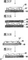
Figure 31 A, 31B, 31C, 31D, 31E, 31F, 31G, 31H and 31I are the sectional views of the forming process of the optical element among the expression embodiment 7.
Figure 32 is the sectional view of the structure of the multilayer diffraction optical element among the expression embodiment 7.
Figure 33 is the curve map of the first-order diffraction light intensity of the multilayer diffraction optical element among the expression embodiment 7.
Figure 34 is the curve map of the light loss rate of the multilayer diffraction optical element among the expression embodiment 7.
Figure 35 A, 35B, 35C, 35D, 35E, 35F, 35G, 35H and 35I are the sectional views of the forming process of the optical element among the expression embodiment 8.
Figure 36 is the sectional view of the structure of the multilayer diffraction optical element among the expression embodiment 8.
Figure 37 is the curve map of the first-order diffraction light intensity of the multilayer diffraction optical element among the expression embodiment 8.
Figure 38 is the curve map of the light loss rate of the multilayer diffraction optical element among the expression embodiment 8.
Figure 39 A, 39B, 39C, 39D, 39E are the sectional views of the forming process of the optical element in the expression comparative example 2.
Figure 40 is the sectional view of the structure of the multilayer diffraction optical element in the expression comparative example 2.
Figure 41 is the curve map of the first-order diffraction light intensity of the multilayer diffraction optical element in the expression comparative example 2.
Figure 42 is the curve map of the light loss rate of the multilayer diffraction optical element in the expression comparative example 2.
Figure 43 is the sectional view of the multilayer diffraction optical element of 3 layers of expressions.
Figure 44 is the mode chart of the projection optical system in the 2nd example.
Figure 45 is the mode chart of the photographic optical system in the 3rd example.
Embodiment
(the 1st example)
Can the present inventor have discussed by being included in the particulate of the inorganic oxide that obsolete Abbe number is little in the common optical material in the optical material of polymkeric substance etc., thereby make the little optical material of Abbe number.As the little inorganic oxide of Abbe number, can consider TiO
2(n
d=2.2652, ν
d=11.8), Nb
2O
5(n
d=2.367, ν
d=14.0), ITO (n
d=1.8581, ν
d=5.53), Cr
2O
3(n
d=2.2178, ν
d=13.4), BaTiO
3(n
d=2.4362, ν
d=11.3) etc.
These inorganic oxides are to constitute the material that prevents reflectance coating usually, and most situations are that their thickness uses in 50~500nm scope.But, adjust shape by vacuum film formation and may be used in the diffraction optical element of the following thickness of 50nm.Again, by with the combination of the UV hardening resin of in market, selling as matrix polymer, can manufacture optical material easily.Also shape be can easily adjust again, refraction optical element and diffraction optical element are applicable to easily.
Again, when using inorganic oxide, the particle diameter of wishing it is 2~100nm.The light scattering of potpourri became big when particle diameter was bigger than 100nm, can not be used as optical element.Again, the quantum effect on particle diameter surface when 2nm is following increases, and can not express the characteristic of inorganic oxide.
As comprising inorganic oxide polymer, can mix equably and the polyvinylcarbazole of chromatic dispersion particulate is best suited for again.The polyvinylcarbazole thing that comprises inorganic oxide is by adding inorganic oxide particle in the N-vinylcarbazole, and its sclerosis is obtained.But, comprise inorganic oxide polymer and be not limited to polyvinylcarbazole, preferably satisfy n as optical material
d>-6.667 * 10
-3ν
d+ 1.70 and ν
d≤ 16 condition.Again, by making Abbe number ν
dBe ν
d≤ 16, can improve the numerical aperture of optical element, also can make the further attenuation of thickness of optical element.Therefore, can more easily use above-mentioned inorganic oxide as optical material.
(embodiment 1)
We illustrate the formation and the manufacture method thereof of the laminated diffraction optical elements among the embodiment 1 with reference to Fig. 2 A~2C, Fig. 3 A~3C, Fig. 4, Fig. 5 and Fig. 6.At first, at the TiO of 100g with 10w% chromatic dispersion mean particle diameter 10nm
2After interpolation 12g polyvinylcarbazole (Tokyo changes into industrial group and makes) and 0.15g light begin agent 1-hydroxyl-hexamethylene-benzene-ketone in the chloroform soln of particulate, remove methenyl choloride by decompression and make optics raw material 2.
Secondly, shown in Fig. 2 A, optics raw material 2 is supplied with the metal die 1 that is processed into the diffraction grating shape.Secondly, shown in Fig. 2 B, glass (BK7) dull and stereotyped 3 is placed on the optics raw material 2, each mould is remained in 70 ℃ the state with UV exposure machine (manufacturing of EX250:HOYA-SCHOTT company) with 20000mJ/cm
2(100mW/cm
2, 200 seconds) shine.After this, shown in Fig. 2 C, make the optical element 2 ' disengaging metal die 1 that has hardened make diffraction optical element 4.This optics raw material 2 carries out polymerization by the UV light stiffening, forms polyvinylcarbazole and TiO
2The optical material of particulate.Again, form this optical element 2 ' the optical characteristics of optical material for (n
d=1.824, ν
d=15.1).This optical characteristics satisfies n simultaneously
d>-6.667 * 10
-3ν
d+ 1.70, ν
d≤ 16 condition.
On the other hand, in order to form another optical element, the preparation optical characteristics is (n
d=1.513, ν
d=51.0) light-hardening resin 6 is as optical material.As shown in Figure 3A, make light-hardening resin 6 flow into the metal die 5 that is processed into the diffraction grating shape.With glass (BK7) dull and stereotyped 7 be placed on it above, shown in Fig. 3 B, pressurize.After this, with unillustrated UV exposure machine (manufacturing of EX250:HOYA-SCHOTT company) among the figure with 3000mJ/cm
2(100mW/cm
2, 30 seconds) shine after, shown in Fig. 3 C, make the light-hardening resin 6 that has hardened break away from metal dies 5 and make diffraction optical element 8.
Secondly, after formation on the diffraction surfaces of diffraction optical element 4 and diffraction optical element 8 prevents reflectance coating, as shown in Figure 4, diffraction grating is made up opposed to each other make laminated diffraction optical elements 10.The 9th, the partition at the interval of decision diffraction optical element 4 and diffraction optical element 8.Each grating space of diffraction optical element 4 and diffraction optical element 8 all is 80.00 μ m.The paddy interbody spacer of the mutual diffraction grating of diffraction optical element 4 and diffraction optical element 8 is 9.89 μ m, the peak-to-peak 1.50 μ m that are spaced apart.The height at the peak of diffraction optical element 4 is 2.78 μ m, and the height at the peak of diffraction optical element 8 is 5.61 μ m.
Fig. 5 is illustrated in the laminated diffraction optical elements 10 of manufacturing, each wavelength of the first-order diffraction light that incident angle is 0 ° (curve map of the intensity of 400nm~700nm).Transverse axis is represented wavelength, and the longitudinal axis is represented diffraction efficiency.In Fig. 5, the diffraction efficiency of laminated diffraction optical elements 10 reaches more than 95% in the scope of the 400nm~3700nm of the Zone Full that uses wavelength, we can say the Wavelength distribution of having represented very good intensity.
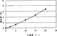
Again, Fig. 6 represents that when changing to the incident angle of laminated diffraction optical elements 10, the secondary diffraction light intensity on each incident angle reduces the curve map of ratio.Transverse axis is represented incident angle, and the longitudinal axis is represented the loss percentage of light.In Fig. 6, the big more loss percentage of incident angle is high more, and still the light loss rate 10 ° of incident angles is 3.27%, below 3.40%.Therefore this value representation very good characteristic, we can say that laminated diffraction optical elements 10 fully concentrates on the specific progression light.
(comparative example 1)
Below, we illustrate the formation and the manufacture method thereof of the laminated diffraction optical elements in the comparative example 1 with reference to Fig. 7 A~7C, Fig. 3 A~3C, Fig. 8, Fig. 9, Figure 10.As a comparative example 1, the N-vinylcarbazole (Tokyo changes into industrial group and makes) that begins agent 1-hydroxyl-hexamethylene-benzene-ketone with the light that adds 1% is made optics raw material 202.
Secondly, shown in Fig. 7 A, optics raw material 202 is supplied with metal die 201.Secondly, shown in Fig. 7 B, be pressed on the optics raw material 202, make each mould remain in 70 ℃ the state among the usefulness figure unillustrated UV exposure machine (manufacturing of EX250:HOYA-SCHOTT company) with 20000mJ/cm with glass (BK7) dull and stereotyped 203
2(100mW/cm
2, 200 seconds) shine.After this, shown in Fig. 7 C, make light-hardening resin 202 break away from metal die 201 and make diffraction optical element 204.Carry out polymerization by this light-hardening resin 202 of UV light stiffening and form the optical material that constitutes by polyvinylcarbazole.The optical characteristics of this optical material is (n
d=1.702, ν
d=17.4).This optical characteristics satisfies n
d>-6.667 * 10
-3ν
d+ 1.70 condition, but do not satisfy ν
d≤ 16 condition.
On the other hand, as the optical material that is used to form another optical element, prepare optical characteristics similarly to Example 1 and be (n
d=1.513, ν
d=51.0) light-hardening resin 6.With making diffraction optical element 8 with the same method of the embodiment 1 shown in Fig. 3 A~3C.
Secondly, after formation on diffraction optical element 204 and the diffraction optical element 8 prevents reflectance coating, as shown in Figure 8, diffraction grating is made up opposed to each other make laminated diffraction optical elements 210.2C9 is the partition at the interval of decision diffraction optical element 204 and diffraction optical element 8.Each grating space of diffraction optical element 204 and diffraction optical element 8 is 80.00 μ m.The paddy interbody spacer of the mutual diffraction grating of diffraction optical element 204 and diffraction optical element 8 is 11.87 μ m, the peak-to-peak 1.50 μ m that are spaced apart.The height at the peak of diffraction optical element 204 is 3.92 μ m, and the height at the peak of diffraction optical element 8 is 6.45 μ m.
Fig. 9 is illustrated in the laminated diffraction optical elements 210 of manufacturing, each wavelength of the first-order diffraction light that incident angle is 0 ° (curve map of the intensity of 400nm~700nm).Transverse axis is represented wavelength, and the longitudinal axis is represented diffraction efficiency.In Fig. 9, the diffraction efficiency of laminated diffraction optical elements 210 reaches more than 95% in the scope of the wavelength 400nm~700nm of the Zone Full that uses wavelength, we can say the Wavelength distribution of having represented very good intensity.
But Figure 10 represents that when changing to the incident angle of laminated diffraction optical elements 210, the secondary diffraction light intensity on each incident angle reduces the curve map of ratio.Transverse axis is represented incident angle, and the longitudinal axis is represented the loss percentage of light.Again in order to compare the value that in Figure 10, has also shown Fig. 6 of embodiment 1 together.In Figure 10, the big more loss percentage of incident angle is high more, is 3.52% in the light loss rate of 10 ° of incident angles.This value is in the value of the light loss rate that requires more than 3.40%.Therefore we can not say that laminated diffraction optical elements 210 fully concentrates on the specific progression light as laminated diffraction optical elements.
(embodiment 2)
Below, we illustrate the formation and the manufacture method thereof of the laminated diffraction optical elements among the embodiment 2 with reference to Figure 11 A~11C, Fig. 3 A~3C, Figure 12, Figure 13, Figure 14.At first, at the Nb of 100g with 10w% chromatic dispersion mean particle diameter 10nm
2O
3After interpolation 12gN-polyvinylcarbazole (Tokyo changes into industrial group and makes) and 0.15g light begin agent 1-hydroxyl-hexamethylene-benzene-ketone in the chloroform soln of particulate, remove methenyl choloride by decompression and make optics raw material 12.
Secondly, shown in Figure 11 A, optics raw material 12 is supplied with the metal die 11 that is processed into the diffraction grating shape.Secondly, shown in Figure 11 B, glass (BK7) dull and stereotyped 13 is placed on the optics raw material 12, each mould is remained in 70 ℃ the state with UV exposure machine (manufacturing of EX250:HOYA-SCHOTT company) with 20000mJ/cm
2(100mW/cm
2, 200 seconds) shine.After this, shown in Figure 11 C, make the optical element 12 ' disengaging metal die 11 that has hardened make diffraction optical element 14.This optics raw material 12 carries out polymerization by the UV light stiffening, forms polyvinylcarbazole and Nb
2O
3The optical material of particulate.Again, form this optical element 12 ' the optical characteristics of optical material for (n
d=1.850, ν
d=16.0).This optical characteristics satisfies n simultaneously
d>-6.667 * 10
-3ν
d+ 1.70, ν
d≤ 16 condition.
On the other hand, as the optical material that is used to form another optical element, prepare optical characteristics similarly to Example 1 and be (n
d=1.513, ν
d=51.0) light-hardening resin 6.With making diffraction optical element 8 with the same method of the embodiment 1 shown in Fig. 3 A~3C.
Secondly, after formation on the diffraction surfaces of diffraction optical element 14 and diffraction optical element 8 prevents reflectance coating, as shown in figure 12, diffraction grating is made up opposed to each other make laminated diffraction optical elements 20.The 19th, the partition at the interval of decision diffraction optical element 14 and diffraction optical element 8.Each grating space of diffraction optical element 14 and diffraction optical element 8 is 80.00 μ m.The paddy interbody spacer of the mutual diffraction grating of diffraction optical element 4 and diffraction optical element 8 is 10.41 μ m, the peak-to-peak 1.50 μ m that are spaced apart.The height at the peak of diffraction optical element 14 is 2.92 μ m, and the height at the peak of diffraction optical element 8 is 5.99 μ m.
Figure 13 is illustrated in the laminated diffraction optical elements 20 of manufacturing, each wavelength of the first-order diffraction light that incident angle is 0 ° (curve map of the intensity of 400nm~700nm).Transverse axis is represented wavelength, and the longitudinal axis is represented diffraction efficiency.In Figure 13, the diffraction efficiency of laminated diffraction optical elements 20 reaches more than 95% in the scope of the wavelength 400nm~700nm of the Zone Full that uses wavelength, we can say the Wavelength distribution of having represented very good intensity.
Again, Figure 14 represents that when changing to the incident angle of laminated diffraction optical elements 20, the secondary diffraction light intensity on each incident angle reduces the curve map of ratio.Transverse axis is represented incident angle, and the longitudinal axis is represented the loss percentage of light.In Figure 14, the big more loss percentage of incident angle is high more, and still the light loss rate 10 ° of incident angles is 3.40%.So the very good characteristic of this value representation, we can say that laminated diffraction optical elements 20 fully concentrates on the specific progression light.
(embodiment 3)
Below, we illustrate the formation and the manufacture method thereof of the laminated diffraction optical elements among the embodiment 3 with reference to Figure 15 A~15C, Fig. 3 A~3C, Figure 16, Figure 17, Figure 18.At first, at the Cr of 130g with 10w% chromatic dispersion mean particle diameter 10nm
2O
5After interpolation 12gN-polyvinylcarbazole (Tokyo changes into industrial group and makes) and 0.15g light begin agent 1-hydroxyl-hexamethylene-benzene-ketone in the chloroform soln of particulate, remove methenyl choloride by decompression and make optics raw material 22.
Secondly, shown in Figure 15 A, optics raw material 22 is supplied with the metal die 21 that is processed into the diffraction grating shape.Secondly, shown in Figure 15 B, glass (BK7) dull and stereotyped 23 is placed on the optics raw material 22, each mould is remained in 70 ℃ the state with UV exposure machine (manufacturing of EX250:HOYA-SCHOTT company) with 20000mJ/cm
2(100mW/cm
2, 200 seconds) shine.After this, shown in Figure 15 C, make the optical element 22 ' disengaging metal die 21 that has hardened make diffraction optical element 24.This optics raw material 22 carries out polymerization by the UV light stiffening, forms polyvinylcarbazole and Cr
2O
5The optical material of particulate.Again, form this optical element 22 ' the optical characteristics of optical material for (n
d=1.824, ν
d=15.9).This optical characteristics satisfies n simultaneously
d>-6.667 * 10
-3ν
d+ 1.70, ν
d≤ 16 condition.
On the other hand, as the optical material that is used to form another optical element, prepare optical characteristics similarly to Example 1 and be (n
d=1.513, ν
d=51.0) light-hardening resin 6.With making diffraction optical element 8 with the same method of the embodiment 1 shown in Fig. 3 A~3C.
Secondly, after formation on the diffraction surfaces of diffraction optical element 24 and diffraction optical element 8 prevents reflectance coating, as shown in figure 16, diffraction grating is made up opposed to each other make laminated diffraction optical elements 30.The 29th, the partition at the interval of decision diffraction optical element 24 and diffraction optical element 8.Each grating space of diffraction optical element 24 and diffraction optical element 8 all is 80.00 μ m.The paddy interbody spacer of the mutual diffraction grating of diffraction optical element 24 and diffraction optical element 8 is 10.50 μ m, the peak-to-peak 1.50 μ m that are spaced apart.The height at the peak of diffraction optical element 24 is 2.94 μ m, and the height at the peak of diffraction optical element 8 is 6.06 μ m.
Figure 17 is illustrated in the laminated diffraction optical elements of making 30, each wavelength of the first-order diffraction light that incident angle is 0 ° (curve map of the intensity of 400nm~700nm).Transverse axis is represented wavelength, and the longitudinal axis is represented diffraction efficiency.In Figure 17, the diffraction efficiency of laminated diffraction optical elements 30 reaches more than 95% in the scope of the wavelength 400nm~700nm of the Zone Full that uses wavelength, we can say the Wavelength distribution of having represented very good intensity.
Again, Figure 18 represents that when changing to the incident angle of laminated diffraction optical elements 30, the secondary diffraction light intensity on each incident angle reduces the curve map of ratio.Transverse axis is represented incident angle, and the longitudinal axis is represented the loss percentage of light.In Figure 18, the big more loss percentage of incident angle is high more, and still the light loss rate 10 ° of incident angles is 3.40%.So the very good characteristic of this value representation, we can say that laminated diffraction optical elements 30 fully concentrates on the specific progression light.
(embodiment 4)
Below, we illustrate the formation and the manufacture method thereof of the laminated diffraction optical elements among the embodiment 4 with reference to Figure 19 A~19C, Fig. 3 A~3C, Figure 20, Figure 21, Figure 22.At first, at the BaTiO of 100g with 10w% chromatic dispersion mean particle diameter 10nm
3After interpolation 12gN-polyvinylcarbazole (Tokyo changes into industrial group and makes) and 0.15g light begin agent 1-hydroxyl-hexamethylene-benzene-ketone in the chloroform soln of particulate, remove methenyl choloride by decompression and make optics raw material 32.
Secondly, shown in Figure 19 A, optics raw material 32 is supplied with the metal die 31 that is processed into the diffraction grating shape.Secondly, shown in Figure 19 B, glass (BK7) dull and stereotyped 33 is placed on the optics raw material 32, each mould is remained in 70 ℃ the state with UV exposure machine (manufacturing of EX250:HOYA-SCHOTT company) with 20000mJ/cm
2(100mW/cm
2, 200 seconds) shine.After this, shown in Figure 19 C, make the optical element 32 ' disengaging metal die 31 that has hardened make diffraction optical element 34.This optics raw material 32 carries out polymerization by the UV light stiffening, forms polyvinylcarbazole and BaTiO
3The optical material of particulate.Again, form this optical element 32 ' the optical characteristics of optical material for (n
d=1.867, ν
d=14.7).This optical characteristics satisfies n simultaneously
d>-6.667 * 10
-3ν
d+ 1.70, ν
d≤ 16 condition.
On the other hand, as the optical material that is used to form another optical element, prepare optical characteristics similarly to Example 1 and be (n
d=1.513, ν
d=51.0) light-hardening resin 6.With making diffraction optical element 8 with the same method of the embodiment 1 shown in Fig. 3 A~3C.
Secondly, after formation on the diffraction surfaces of diffraction optical element 34 and diffraction optical element 8 prevents reflectance coating, as shown in figure 20, diffraction grating is made up opposed to each other make laminated diffraction optical elements 40.The 39th, the partition at the interval of decision diffraction optical element 34 and diffraction optical element 8.Each grating space of diffraction optical element 34 and diffraction optical element 8 all is 80.00 μ m.The paddy interbody spacer of the mutual diffraction grating of diffraction optical element 34 and diffraction optical element 8 is 9.60 μ m, the peak-to-peak 1.50 μ m that are spaced apart.The height at the peak of diffraction optical element 34 is 2.64 μ m, and the height at the peak of diffraction optical element 8 is 5.46 μ m.
Figure 21 is illustrated in the laminated diffraction optical elements of making 40, each wavelength of the first-order diffraction light that incident angle is 0 ° (curve map of the intensity of 400nm~700nm).Transverse axis is represented wavelength, and the longitudinal axis is represented diffraction efficiency.In Figure 21, the diffraction efficiency of laminated diffraction optical elements 40 reaches more than 95% in the scope of the wavelength 400nm~700nm of the Zone Full that uses wavelength, we can say the Wavelength distribution of having represented very good intensity.
Again, Figure 22 represents that when changing to the incident angle of laminated diffraction optical elements 40, the secondary diffraction light intensity on each incident angle reduces the curve map of ratio.Transverse axis is represented incident angle, and the longitudinal axis is represented the loss percentage of light.In Figure 22, the big more loss percentage of incident angle is high more, and still the light loss rate 10 ° of incident angles is 3.24%, below 3.40%.So the very good characteristic of this value representation, we can say that laminated diffraction optical elements 40 fully concentrates on the specific progression light.
(embodiment 5)
Below, we illustrate the formation and the manufacture method thereof of the laminated diffraction optical elements among the embodiment 5 with reference to Figure 23 A~23C, Fig. 3 A~3C, Figure 24, Figure 25, Figure 26.At first, add and to have added the methacrylic acid methyl that 1% light begins agent 1-hydroxyl-hexamethylene-benzene-ketone and make optics raw material 42.Secondly, shown in Figure 23 A, optics raw material 42 is supplied with the metal die 41 that is processed into the diffraction grating shape.Secondly, shown in Figure 23 B, glass (BK7) dull and stereotyped 43 is placed on the optics raw material 42, uses UV exposure machine (manufacturing of EX250:HOYA-SCHOTT company) with 3000mJ/cm
2(100mW/cm
2, 30 seconds) shine.After this, shown in Figure 23 C, make the optical element 42 ' that has hardened break away from metal die 41 and make the diffraction optical element 44 shown in Figure 23 D.After this, shown in Figure 23 E, in vacuum tightness 2 * 10
-4Go up the TiO that forms 4 μ m as optical material at optical element 42 ' among the Pa
2Film 45.Secondly shown in Figure 23 F, by grinding TiO
2The surface of film 45 forms the following plane of 1 newton's line.After this, shown in Figure 23 G, the glass plate 46 that has applied silane adhesive is bonded in TiO
2On the film 45.After this, shown in Figure 23 H, make the PMMA dissolving of sclerosis by adding the hexone solvent, make shown in Figure 23 I by TiO
2The diffraction grating shape 47 that constitutes.TiO as at this moment optical material
2Optical characteristics be (n
d=2.226, ν
d=12.6).
On the other hand, as the optical material that is used to form another optical element, prepare optical characteristics similarly to Example 1 and be (n
d=1.513, ν
d=51.0) light-hardening resin 6.With making diffraction optical element 8 with the same method of the embodiment 1 shown in Fig. 3 A~3C.
Secondly, after formation on the diffraction surfaces of diffraction optical element 47 and diffraction optical element 8 prevents reflectance coating, as shown in figure 24, diffraction grating is made up opposed to each other make laminated diffraction optical elements 50.The 49th, the partition at the interval of decision diffraction optical element 47 and diffraction optical element 8.Each grating space of diffraction optical element 47 and diffraction optical element 8 all is 80.00 μ m.The paddy interbody spacer of the mutual diffraction grating of diffraction optical element 47 and diffraction optical element 8 is 7.80 μ m, the peak-to-peak 1.50 μ m that are spaced apart.The height at the peak of diffraction optical element 47 is 1.48 μ m, and the height at the peak of diffraction optical element 8 is 4.82 μ m.
Figure 25 is illustrated in the laminated diffraction optical elements of making 50, each wavelength of the first-order diffraction light that incident angle is 0 ° (curve map of the intensity of 400nm~700nm).Transverse axis is represented wavelength, and the longitudinal axis is represented diffraction efficiency.In Figure 25, the diffraction efficiency of laminated diffraction optical elements 50 reaches more than 95% in the scope of the wavelength 400nm~700nm of the Zone Full that uses wavelength, we can say the Wavelength distribution of having represented very good intensity.
Again, Figure 26 represents that when changing to the incident angle of laminated diffraction optical elements 50, the secondary diffraction light intensity on each incident angle reduces the curve map of ratio.Transverse axis is represented incident angle, and the longitudinal axis is represented the loss percentage of light.In Figure 26, the big more loss percentage of incident angle is high more, and still the light loss rate 10 ° of incident angles is 3.06%, below 3.40%.So the very good characteristic of this value representation, we can say that laminated diffraction optical elements 50 fully concentrates on the specific progression light.
(embodiment 6)
Below, we illustrate the formation and the manufacture method thereof of the laminated diffraction optical elements among the embodiment 6 with reference to Figure 27 A~27C, Fig. 3 A~3C, Figure 28, Figure 29, Figure 30.At first, add and to have added the methacrylic acid methyl that 1% light begins agent 1-hydroxyl-hexamethylene-benzene-ketone and make optics raw material 52.Secondly, shown in Figure 27 A, optics raw material 52 is supplied with the metal die 51 that is processed into the diffraction grating shape.Secondly, shown in Figure 27 B, glass (BK7) dull and stereotyped 53 is placed on the optics raw material 52, uses UV exposure machine (manufacturing of EX250:HOYA-SCHOTT company) with 3000mJ/cm
2(100mW/cm
2, 30 seconds) shine.After this, shown in Figure 27 C, make the optical element 52 ' disengaging metal die 51 that has hardened make the diffraction optical element 54 shown in Figure 27 D.After this, shown in Figure 27 E, in vacuum tightness 2 * 10
-4Among the Pa optical element 52 ' on form the TiO of 4 μ m as optical material
2Film 55.Secondly shown in Figure 27 F, by grinding Nb
2O
3The surface of film 55 forms the following plane of 1 newton's line.After this, shown in Figure 27 G, the glass plate 56 that has applied silane adhesive is bonded in Nb
2O
3On the film 55.After this, shown in Figure 27 H, make the PMMA dissolving of sclerosis by adding the hexone solvent, make shown in Figure 27 I by Nb
2O
3The diffraction grating shape 57 that constitutes.Nb as at this moment optical material
2O
3Optical characteristics be (n
d=2.367, ν
d=14.6).
On the other hand, as the optical material that is used to form another optical element, prepare optical characteristics similarly to Example 1 and be (n
d=1.513, ν
d=51.0) light-hardening resin 6.With making diffraction optical element 8 with the same method of the embodiment 1 shown in Fig. 3 A~3C.
Secondly, after formation on the diffraction surfaces of diffraction optical element 57 and diffraction optical element 8 prevents reflectance coating, as shown in figure 28, diffraction grating is made up opposed to each other make laminated diffraction optical elements 60.The 59th, the partition at the interval of decision diffraction optical element 57 and diffraction optical element 8.Each grating space of diffraction optical element 57 and diffraction optical element 8 all is 80.00 μ m.The paddy interbody spacer of the mutual diffraction grating of diffraction optical element 57 and diffraction optical element 8 is 8.81 μ m, the peak-to-peak 1.5 μ m that are spaced apart.The height at the peak of diffraction optical element 57 is 1.68 μ m, and the height at the peak of diffraction optical element 8 is 5.63 μ m.
Figure 29 is illustrated in the laminated diffraction optical elements of making 60, each wavelength of the first-order diffraction light that incident angle is 0 ° (curve map of the intensity of 400nm~700nm).Transverse axis is represented wavelength, and the longitudinal axis is represented diffraction efficiency.In Figure 29, the diffraction efficiency of laminated diffraction optical elements 60 reaches more than 95% in the scope of the wavelength 400nm~700nm of the Zone Full that uses wavelength, we can say the Wavelength distribution of having represented very good intensity.
Again, Figure 30 represents that when changing to the incident angle of laminated diffraction optical elements 60, the secondary diffraction light intensity on each incident angle reduces the curve map of ratio.Transverse axis is represented incident angle, and the longitudinal axis is represented the loss percentage of light.In Figure 30, the big more loss percentage of incident angle is high more, and still the light loss rate 10 ° of incident angles is 3.15%, below 3.40%.So the very good characteristic of this value representation, we can say that laminated diffraction optical elements 60 fully concentrates on the specific progression light.
(embodiment 7)
Below, we illustrate the formation and the manufacture method thereof of the laminated diffraction optical elements among the embodiment 7 with reference to Figure 31 A~31C, Fig. 3 A~3C, Figure 32, Figure 33, Figure 34.At first, add and to have added the methacrylic acid methyl that 1% light begins agent 1-hydroxyl-hexamethylene-benzene-ketone and make optics raw material 62.Secondly, shown in Figure 31 A, optics raw material 62 is supplied with the metal die 61 that is processed into the diffraction grating shape.Secondly, shown in Figure 31 B, glass (BK7) dull and stereotyped 63 is placed on the optics raw material 62, uses UV exposure machine (manufacturing of EX250:HOYA-SCHOTT company) with 3000mJ/cm
2(100mW/cm
2, 30 seconds) shine.After this, shown in Figure 31 C, make the optical element 62 ' disengaging metal die 61 that has hardened make the diffraction optical element 64 shown in Figure 31 D.After this, shown in Figure 31 E, in vacuum tightness 2 * 10
-4Among the Pa optical element 62 ' on form the Cr of 4 μ m as optical material
2O
5Film 65.Secondly shown in Figure 31 F, by grinding Cr
2O
5The surface of film 65 forms the following plane of 1 newton's line.After this, shown in Figure 31 G, the glass plate 66 that has applied silane adhesive is bonded in Cr
2O
5On the film 65.After this, shown in Figure 31 H, make the PMMA dissolving of sclerosis by adding the hexone solvent, make shown in Figure 31 I by Cr
2O
5The diffraction grating shape 67 that constitutes.Cr as at this moment optical material
2O
5Optical characteristics be (n
d=2.218, ν
d=14.2).
On the other hand, as the optical material that is used to form another optical element, prepare optical characteristics similarly to Example 1 and be (n
d=1.513, ν
d=51.0) light-hardening resin 6.With making diffraction optical element 8 with the same method of the embodiment 1 shown in Fig. 3 A~3C.
Secondly, after formation on the diffraction surfaces of diffraction optical element 67 and diffraction optical element 8 prevents reflectance coating, shown in figure 32, diffraction grating is made up opposed to each other make laminated diffraction optical elements 70.The 69th, the partition at the interval of decision diffraction optical element 67 and diffraction optical element 8.Each grating space of diffraction optical element 67 and diffraction optical element 8 all is 80.00 μ m.The paddy interbody spacer of the mutual diffraction grating of diffraction optical element 67 and diffraction optical element 8 is 8.80 μ m, the peak-to-peak 1.5 μ m that are spaced apart.The height at the peak of diffraction optical element 67 is 1.70 μ m, and the height at the peak of diffraction optical element 8 is 5.60 μ m.
Figure 33 is illustrated in the laminated diffraction optical elements of making 70, each wavelength of the first-order diffraction light that incident angle is 0 ° (curve map of the intensity of 400nm~700nm).Transverse axis is represented wavelength, and the longitudinal axis is represented diffraction efficiency.In Figure 33, the diffraction efficiency of laminated diffraction optical elements 70 reaches more than 95% in the scope of the wavelength 400nm~700nm of the Zone Full that uses wavelength, we can say the Wavelength distribution of having represented very good intensity.
Again, Figure 34 represents that when changing to the incident angle of laminated diffraction optical elements 70, the secondary diffraction light intensity on each incident angle reduces the curve map of ratio.Transverse axis is represented incident angle, and the longitudinal axis is represented the loss percentage of light.In Figure 34, the big more loss percentage of incident angle is high more, and still the light loss rate 10 ° of incident angles is 3.15%, at 3.40 following %.So the very good characteristic of this value representation, we can say that laminated diffraction optical elements 70 fully concentrates on the specific progression light.
(embodiment 8)
Below, we illustrate the formation and the manufacture method thereof of the laminated diffraction optical elements among the embodiment 8 with reference to Figure 35 A~35C, Fig. 3 A~3C, Figure 36, Figure 37, Figure 38.At first, add and to have added the methacrylic acid methyl that 1% light begins agent 1-hydroxyl-hexamethylene-benzene-ketone and make optics raw material 72.Secondly, shown in Figure 35 A, optics raw material 72 is supplied with the metal die 71 that is processed into the diffraction grating shape.Secondly, shown in Figure 35 B, glass (BK7) dull and stereotyped 73 is placed on the optics raw material 72, with UV exposure machine (manufacturing of EX250:HOYA-SCHOTT company) 3000mJ/cm
2(100mW/cm
2, 30 seconds) shine.After this, shown in Figure 35 C, make the optical element 72 ' disengaging metal die 71 that has hardened make the diffraction optical element 74 shown in Figure 35 D.After this, shown in Figure 35 E, in vacuum tightness 2 * 10
-4Among the Pa optical element 72 ' on form the BaTiO of 4 μ m as optical material
3Film 75.Secondly shown in Figure 35 F, by grinding BaTiO
3The surface of film 75 forms the following plane of 1 newton's line.After this, shown in Figure 35 G, the glass plate 76 that has applied silane adhesive is bonded in BaTiO
3On the film 75.After this, shown in Figure 35 H, make the PMMA dissolving of sclerosis by adding the hexone solvent, make shown in Figure 35 I by BaTiO
3The diffraction grating shape 77 that film 75 constitutes.BaTiO as at this moment optical material
3Optical characteristics be (n
d=2.436, ν
d=12.4).
On the other hand, as the optical material that is used to form another optical element, prepare optical characteristics similarly to Example 1 and be (n
d=1.513, ν
d=51.0) light-hardening resin 6.With making diffraction optical element 8 with the same method of the embodiment 1 shown in Fig. 3 A~3C.
Secondly, after formation on the diffraction surfaces of diffraction optical element 77 and diffraction optical element 8 prevents reflectance coating, as shown in figure 36, diffraction grating is made up opposed to each other make laminated diffraction optical elements 80.The 79th, the partition at the interval of decision diffraction optical element 77 and diffraction optical element 8.Each grating space of diffraction optical element 77 and diffraction optical element 8 all is 80.00 μ m.The paddy interbody spacer of the mutual diffraction grating of diffraction optical element 77 and diffraction optical element 8 is 6.33 μ m, the peak-to-peak 1.5 μ m that are spaced apart.The height at the peak of diffraction optical element 77 is 0.97 μ m, and the height at the peak of diffraction optical element 8 is 3.86 μ m.
Figure 37 is illustrated in the laminated diffraction optical elements of making 80, each wavelength of the first-order diffraction light that incident angle is 0 ° (curve map of the intensity of 400nm~700nm).Transverse axis is represented wavelength, and the longitudinal axis is represented diffraction efficiency.In Figure 37, the diffraction efficiency of laminated diffraction optical elements 80 reaches more than 95% in the scope of the wavelength 400nm~700nm of the Zone Full that uses wavelength, we can say the Wavelength distribution of having represented very good intensity.
Again, Figure 38 represents that when changing to the incident angle of laminated diffraction optical elements 80, the secondary diffraction light intensity on each incident angle reduces the curve map of ratio.Transverse axis is represented incident angle, and the longitudinal axis is represented the loss percentage of light.In Figure 38, the big more loss percentage of incident angle is high more, and still the light loss rate 10 ° of incident angles is 3.00%, at 3.40 following %.So the very good characteristic of this value representation, we can say that laminated diffraction optical elements 80 fully concentrates on the specific progression light.
(comparative example 2)
Below, we illustrate the formation and the manufacture method thereof of the laminated diffraction optical elements in the comparative example 2 with reference to Figure 39 A~39C, Fig. 3 A~3C, Figure 40, Figure 41, Figure 42.As a comparative example 2, at the TiO of 100g with 10w% chromatic dispersion mean particle diameter 10nm
2In the fluorine series solvent of particulate, add 13.8g and make optics raw material 212 by the amorphous fluororesin of the compound structure of following general expression (1) expression.
General expression (1)
Secondly, shown in Figure 39 A, make optics raw material 212 flow into the metal die 211 that is processed into the diffraction grating shape.Secondly, shown in Figure 39 B, make its about 70% evaporation by solvent composition at 70 ℃ of heating optics raw materials 212.After this, shown in Figure 39 C, glass (BK7) dull and stereotyped 213 is placed on the optics raw material 212, shown in Figure 39 D, is configured in the vacuum chamber 215, the state that each metal die 211 is remained on 70 ℃ kept 48 hours at the vacuum state of 2hPa.After this, shown in Figure 39 E, make the optical element 212 ' disengaging metal die 2111 that has hardened make diffraction optical element 214.Again, form this optical element 212 ' the optical characteristics of optical material for (n
d=1.589, ν
d=15.0).This optical characteristics satisfies ν
d≤ 16, but do not satisfy n
d>-6.667 * 10
-3ν
d+ 1.70.
On the other hand, as the optical material that is used to form another optical element, prepare optical characteristics similarly to Example 1 and be (n
d=1.513, ν
d=51.0) light-hardening resin 6.With making diffraction optical element 8 with the same method of the embodiment 1 shown in Fig. 3 A~3C.
Secondly, after formation on the diffraction surfaces of diffraction optical element 214 and diffraction optical element 8 prevents reflectance coating, as shown in figure 40, diffraction grating is made up opposed to each other make laminated diffraction optical elements 220.The 219th, the partition at the interval of decision diffraction optical element 214 and diffraction optical element 8.Each grating space of diffraction optical element 214 and diffraction optical element 8 is 80.00 μ m.The paddy interbody spacer of the mutual diffraction grating of diffraction optical element 214 and diffraction optical element 8 is 11.49 μ m, the peak-to-peak 1.50 μ m that are spaced apart.The height at the peak of diffraction optical element 214 is 4.11 μ m, and the height at the peak of diffraction optical element 8 is 5.87 μ m.
Figure 41 is illustrated in the laminated diffraction optical elements of making 220, each wavelength of the first-order diffraction light that incident angle is 0 ° (curve map of the intensity of 400nm~700nm).Transverse axis is represented wavelength, and the longitudinal axis is represented diffraction efficiency.In Figure 41, the diffraction efficiency of laminated diffraction optical elements 220 reaches more than 95% in the scope of the wavelength 400nm~700nm of the Zone Full that uses wavelength, we can say the Wavelength distribution of having represented very good intensity.
But Figure 42 represents that when changing to the incident angle of laminated diffraction optical elements 220, the secondary diffraction light intensity on each incident angle reduces the curve map of ratio.Transverse axis is represented incident angle, and the longitudinal axis is represented the loss percentage of light.Again in order to compare the value that also demonstrates Fig. 6 of embodiment 1 together.In Figure 42, the big more loss percentage of incident angle is high more, and still the light loss rate 10 ° of incident angles is 3.48%.This value is in the light loss rate value that requires more than 3.40%.Therefore we can not say that laminated diffraction optical elements 220 fully concentrates on the specific progression light as laminated diffraction optical elements.
Next, the light loss rate that the incident angle of table 1 expression the above embodiments 1~8 and comparative example 1~2 is 10 °.Condition 1 is n in table 1
d>-6.667 * 10
-3ν
d+ 1.70, condition 2 is ν
d≤ 16.Because to the laminated diffraction optical elements requirement be light loss rate 10 ° of incident angles below 3.40%, so to whether good judgement by whether 3.40% to make decision.
Table 1
| | | The light loss rate that incident angle is 10 ° | Whether | |
| Embodiment | ||||
| 1 | ????○ | ????○ | ????3.27% | ????○ |
| | ????○ | ????○ | ????3.40% | ????○ |
| | ????○ | ????○ | ????3.40% | ????○ |
| | ????○ | ????○ | ????3.24% | ????○ |
| | ????○ | ????○ | ????3.06% | ????○ |
| | ????○ | ????○ | ????3.15% | ????○ |
| | ????○ | ????○ | ????3.15% | ????○ |
| | ????○ | ????○ | ????3.00% | ????○ |
| Comparative example 1 | ????○ | ????× | ????3.52% | ????× |
| Comparative example 2 | ????× | ????○ | ????3.48% | ????× |
As can be seen from Table 1, in the optical material of embodiment 1~8, with the optical element comparison of comparative example 1~2, the light loss rate that incident angle is 10 ° is little, and light is fully concentrated on the specific progression.That is, as the n that does not satisfy as condition 1
d>-6.667 * 10
-3ν
d+ 1.70 and are ν as condition 2
dDuring in≤16 at least one, can not reach desired light loss rate, light is fully concentrated on the specific progression.
Again, we have stated the 2 stratotype diffraction optical elements that the diffraction surfaces that makes them disposes 2 stratotype diffraction optical elements opposed to each other in this example, but the invention is not restricted to this, also can use the laminated diffraction optical elements of diffraction optical element more than 3 or layer laminate ground configuration.Figure 43 is the sectional view of an example of the laminated diffraction optical elements 90 of 3 layers of expressions.In Figure 43, the 7th, glass substrate, 81 is the 1st layer, and 82 is the 2nd layer, and 83 is the 3rd layer.The 1st layer 81 is by satisfying the n shown in the above embodiments 1~8
d>-6.667 * 10
-3ν
d+ 1.70 and ν
dThe optical material of≤16 conditions forms.Form Abbe number that the 2nd layer 82, the 3rd layers 83 optical material has it than the big value of Abbe number that forms the 1st layer 81 optical material.Has the more optical element of sophisticated functions by increasing the number of plies of diffraction optical element, can making.
(the 2nd example)
The 2nd example is the situation that the diffraction optical element shown in above-mentioned the 1st example is used for projection optical system.Figure 44 represents projection optical system 93.In Figure 44, the 91st, light source, the 92nd, beam-splitter, the 98th, lens barrel, the 94th, lens, the 95th, diffraction optical element of the present invention, the 96th, wafer, the 97th, wafer station.
Diffraction optical element 95 is provided with for the aberration of correcting lens 94.By wafer station 97 wafer 96 is on the desired position, by unillustrated focus detecting device among the figure, with the wafer height control on focal position.Here, corresponding with situation, by unillustrated detection system among the figure, make the following mask registration that has exposed on beam-splitter 92 and the wafer.When focusing on and aim at when finishing, open unillustrated shutter among the figure, use illumination light sub irradiation tabula rasa from light source 91, by projection optical system 98 with the circuit pattern shadow-mark on the beam-splitter 92 on the resist of wafer 96.
Form a plurality of devices through the wafer 96 of like this exposure through well-known known development treatment operation and etching procedure.Optical system with optical element relevant with the present invention can be applied to form the optical device of visual usefulness and illuminating lighting device etc. too.As optical element of the present invention, also can use diffraction optical element optical element in addition with the shape of wanting again.
(the 3rd example)
The 3rd example is the situation that the diffraction optical element shown in above-mentioned the 1st example is used for photographic optical system.Figure 45 represents photographic optical system.In Figure 45, photographic optical system 108 has each element of diffraction optical element 105 more than at least 1, refraction optical element 103, aperture 104.Figure 45 represents to make the state of light beam imaging on light accepting part branch (imaging device) 106 from object that incides photographic optical system 108.
Obtain the good optical characteristic for the diffraction light of the design progression that makes diffraction optical element 105 and refraction optical element 103 synthesize in the certain wavelengths zone, this diffraction light is carried out aberration correction.Light accepting part divides 106 to be made of a plurality of photoreceptors with different spectral sensitivities, and the image that forms synthetic photoreceptor from different spectral sensitivities obtains the formation of color image.Divide 106 eyes etc. that can use burnt sheet photoreceptor of CCD, silver salt and people usually as light accepting part again.
If according to the present invention, then pass through the refractive index (n of d line
d) and Abbe number (ν
d) the pass be n
d>-6.667 * 10
-3ν
d+ 1.70 and Abbe number (ν
d) be ν
d≤ 16 optical element can be provided at the high optical element of the diffraction efficiency of respectively using wavelength region may in whole visibility regions.Again, the light of specific progression (design progression) is fully concentrated in the Zone Full that uses wavelength, improve the diffraction light intensity of diffraction progression.Again therefore, can prevent to design light and the light that designs progression beyond the progression at different local imaging generation hot spot light.
Claims (21)
1. optical material is characterized in that satisfying following condition:
Refractive index to the d line is n in season
d, be ν to the Abbe number of d line
dThe time, have n
d>-6.667 * 10
-3ν
d+ 1.70; ν
d≤ 16.
2. optical material according to claim 1 is characterized in that: by TiO
2, Nb
2O
5, Cr
2O
3, BaTiO
3In at least a dead matter constitute.
3. optical material according to claim 1 is characterized in that: the polymkeric substance that contains inorganic particles.
4. optical material according to claim 3 is characterized in that:
The particle diameter of above-mentioned inorganic particles is 2~100nm.
5. optical material according to claim 4 is characterized in that:
Above-mentioned polymkeric substance is a polyvinylcarbazole, and above-mentioned inorganic particles is TiO
2Particulate, Nb
2O
5Particulate, Cr
2O
3Particulate, BaTiO
3At least a in the particulate.
6. an optical element is made of the described optical material of claim 1, it is characterized in that:
This optical element is configured as predetermined shape by sclerous reaction.
7. optical element according to claim 6 is characterized in that:
One side's surface is the diffraction surfaces with diffractive shape.
8. laminated diffraction optical elements is characterized in that being made of following elements:
The 1st diffraction optical element, the surface of one side are the diffraction surfaces with diffractive shape, and are n by the refractive index to the d line in season
d, be ν to the Abbe number of d line
dThe time, n
d>-6.667 * 10
-3ν
d+ 1.70, ν
d≤ 16 optical material forms,
The 2nd diffraction optical element, its Abbe number is bigger than the 1st diffraction optical element, and the surface of one side is the diffraction surfaces with diffractive shape, and this diffraction surfaces is configured to stand facing each other mutually with the diffraction surfaces of the 1st diffraction optical element.
9. laminated diffraction optical elements according to claim 8 is characterized in that: forming above-mentioned the 1st layer optical material is by TiO
2, Nb
2O
5, Cr
2O
3, BaTiO
3In at least a dead matter constitute.
10. laminated diffraction optical elements according to claim 8 is characterized in that: forming above-mentioned the 1st layer optical material is the polymkeric substance that contains inorganic particles.
11. laminated diffraction optical elements according to claim 10 is characterized in that:
The particle diameter of above-mentioned inorganic particles is 2~100nm.
12. laminated diffraction optical elements according to claim 11 is characterized in that:
Above-mentioned polymkeric substance is a polyvinylcarbazole, and above-mentioned inorganic particles is TiO
2Particulate, Nb
2O
5Particulate, Cr
2O
3Particulate, BaTiO
3A kind of in the particulate.
13. an image pickup optical system is characterized in that: take predetermined object by the described laminated diffraction optical elements of claim 8.
14. a projection optical system is characterized in that: light is projected on the predetermined object by the described laminated diffraction optical elements of claim 8.
15. a laminated diffraction optical elements constitutes by 2 layers at least, each layer formed by different optical materials, it is characterized in that being made of following layer:
The 1st layer, the surface of one side is the diffraction surfaces with diffractive shape, and is n by the refractive index to the d line in season
d, be ν to the Abbe number of d line
dThe time, n
d>-6.667 * 10
-3ν
d+ 1.70, ν
d≤ 16 the 1st optical material forms;
The 2nd layer, it is layered in the 1st layer upper strata or lower floor and disposes, and the surface of one side is the diffraction surfaces with diffractive shape, and is formed than the big optical material of optical element that forms the 1st layer by Abbe number.
16. laminated diffraction optical elements according to claim 15 is characterized in that: forming above-mentioned the 1st layer optical material is by TiO
2, Nb
2O
5, Cr
2O
3, BaTiO
3In at least a dead matter constitute.
17. laminated diffraction optical elements according to claim 15 is characterized in that: forming above-mentioned the 1st layer optical material is the polymkeric substance that contains inorganic particles.
18. laminated diffraction optical elements according to claim 17 is characterized in that:
The particle diameter of above-mentioned inorganic particles is 2~100nm.
19. laminated diffraction optical elements according to claim 18 is characterized in that:
Above-mentioned polymkeric substance is a polyvinylcarbazole, and above-mentioned inorganic particles is TiO
2Particulate, Nb
2O
5Particulate, Cr
2O
3Particulate, BaTiO
3A kind of in the particulate.
20. an image pickup optical system is characterized in that: take predetermined object by the described laminated diffraction optical elements of claim 15.
21. a projection optical system is characterized in that: light is projected on the predetermined object by the described laminated diffraction optical elements of claim 15.
Applications Claiming Priority (4)
| Application Number | Priority Date | Filing Date | Title |
|---|---|---|---|
| JP254712/2002 | 2002-08-30 | ||
| JP2002254712 | 2002-08-30 | ||
| JP2003198460A JP4411026B2 (en) | 2002-08-30 | 2003-07-17 | Optical material, optical element, diffractive optical element, laminated diffractive optical element, optical system |
| JP198460/2003 | 2003-08-17 |
Publications (1)
| Publication Number | Publication Date |
|---|---|
| CN1495440A true CN1495440A (en) | 2004-05-12 |
Family
ID=31497703
Family Applications (1)
| Application Number | Title | Priority Date | Filing Date |
|---|---|---|---|
| CNA031557023A Pending CN1495440A (en) | 2002-08-30 | 2003-08-29 | Optical material, optical element, optical system stacked diffraction optical element |
Country Status (5)
| Country | Link |
|---|---|
| US (1) | US7046445B2 (en) |
| EP (1) | EP1394573B1 (en) |
| JP (1) | JP4411026B2 (en) |
| CN (1) | CN1495440A (en) |
| DE (1) | DE60331508D1 (en) |
Families Citing this family (16)
| Publication number | Priority date | Publication date | Assignee | Title |
|---|---|---|---|---|
| JP4266732B2 (en) * | 2002-08-30 | 2009-05-20 | キヤノン株式会社 | Multilayer diffractive optical element |
| JP4673120B2 (en) * | 2004-04-28 | 2011-04-20 | キヤノン株式会社 | Diffractive optical element and optical system having the same |
| US20060046204A1 (en) * | 2004-08-31 | 2006-03-02 | Sharp Laboratories Of America, Inc. | Directly patternable microlens |
| JP4630645B2 (en) * | 2004-11-19 | 2011-02-09 | キヤノン株式会社 | Optical system |
| JP2008527593A (en) * | 2005-01-11 | 2008-07-24 | コーニンクレッカ フィリップス エレクトロニクス エヌ ヴィ | Optical scanning device |
| JP4077508B2 (en) * | 2005-08-29 | 2008-04-16 | 松下電器産業株式会社 | Lens manufacturing method |
| JP4898205B2 (en) * | 2005-12-08 | 2012-03-14 | キヤノン株式会社 | Optical system and optical apparatus having the same |
| US8015237B2 (en) * | 2006-05-15 | 2011-09-06 | Apple Inc. | Processing of metadata content and media content received by a media distribution system |
| JP4847351B2 (en) * | 2007-01-11 | 2011-12-28 | キヤノン株式会社 | Diffractive optical element and diffraction grating using the same |
| EP1947488B1 (en) * | 2007-01-22 | 2010-05-12 | Canon Kabushiki Kaisha | Laminated diffraction optical element |
| JP4860500B2 (en) | 2007-02-13 | 2012-01-25 | 株式会社 ニコンビジョン | Achromatic lens system, optical device |
| JP5424623B2 (en) * | 2008-01-21 | 2014-02-26 | キヤノン株式会社 | Resin composition and optical element, diffractive optical element and laminated diffractive optical element molded thereby |
| JP2009256462A (en) * | 2008-04-16 | 2009-11-05 | Olympus Corp | Optical material composition and optical element using the same |
| JP2009280731A (en) * | 2008-05-23 | 2009-12-03 | Olympus Corp | Material composition for optical use and optical element using the same |
| US20140093692A1 (en) * | 2012-09-28 | 2014-04-03 | Soken Chemical & Engineering Co., Ltd. | Resin Mold, Production Process Therefor and Uses Thereof |
| CZ307952B6 (en) * | 2015-03-25 | 2019-09-11 | Univerzita Palackého v Olomouci | Refractive afocal optical system for correcting colour defects of diffractive imaging elements |
Family Cites Families (20)
| Publication number | Priority date | Publication date | Assignee | Title |
|---|---|---|---|---|
| US3914129A (en) * | 1972-09-05 | 1975-10-21 | Eastman Kodak Co | High index optical glass |
| US5048925A (en) * | 1985-05-28 | 1991-09-17 | Advanced Environmental Research Group | Quasi volume diffracting structures |
| JP2774168B2 (en) | 1989-12-20 | 1998-07-09 | オリンパス光学工業株式会社 | Phase grating member |
| US5847877A (en) * | 1994-09-12 | 1998-12-08 | Olympus Optical Co., Ltd. | Diffractive optical element |
| JP3717555B2 (en) | 1994-09-12 | 2005-11-16 | オリンパス株式会社 | Diffractive optical element |
| US6061110A (en) * | 1994-10-18 | 2000-05-09 | Kabushiki Kaisha Toshiba | Reflection type liquid crystal display device and method of manufacturing the same |
| JP3618464B2 (en) | 1995-08-29 | 2005-02-09 | オリンパス株式会社 | Diffractive optical element and optical apparatus using the same |
| US6157488A (en) * | 1995-08-29 | 2000-12-05 | Olympus Optical Company Ltd. | Diffractive optical element |
| US6606200B1 (en) * | 1996-09-19 | 2003-08-12 | Canon Kabushiki Kaisha | Zoom lens device and optical apparatus provided with the same |
| JP3472092B2 (en) * | 1997-07-28 | 2003-12-02 | キヤノン株式会社 | Diffractive optical element and optical system using the same |
| JP3495884B2 (en) | 1997-07-28 | 2004-02-09 | キヤノン株式会社 | Diffractive optical element and optical system using the same |
| JP4439608B2 (en) * | 1997-12-24 | 2010-03-24 | キヤノン株式会社 | Viewfinder optical system |
| JP3472154B2 (en) | 1998-09-17 | 2003-12-02 | キヤノン株式会社 | Diffractive optical element and optical system having the same |
| US6560019B2 (en) * | 1998-02-05 | 2003-05-06 | Canon Kabushiki Kaisha | Diffractive optical element and optical system having the same |
| JP3950571B2 (en) * | 1999-03-10 | 2007-08-01 | キヤノン株式会社 | Imaging optical system |
| JP3517625B2 (en) * | 1999-07-01 | 2004-04-12 | キヤノン株式会社 | Optical material and optical system using the same |
| JP3588283B2 (en) * | 1999-09-24 | 2004-11-10 | 松下電器産業株式会社 | Projection lens and projector using it |
| US6778240B2 (en) * | 2000-03-28 | 2004-08-17 | Fuji Photo Film Co., Ltd. | Anti-glare and anti-reflection film, polarizing plate, and image display device |
| EP1376161B1 (en) * | 2002-06-17 | 2008-10-15 | Canon Kabushiki Kaisha | Diffractive optical element and optical system provided with the same |
| JP4266732B2 (en) * | 2002-08-30 | 2009-05-20 | キヤノン株式会社 | Multilayer diffractive optical element |
-
2003
- 2003-07-17 JP JP2003198460A patent/JP4411026B2/en not_active Expired - Fee Related
- 2003-08-28 US US10/649,632 patent/US7046445B2/en not_active Expired - Fee Related
- 2003-08-29 DE DE60331508T patent/DE60331508D1/en not_active Expired - Lifetime
- 2003-08-29 EP EP03019779A patent/EP1394573B1/en not_active Expired - Lifetime
- 2003-08-29 CN CNA031557023A patent/CN1495440A/en active Pending
Also Published As
| Publication number | Publication date |
|---|---|
| DE60331508D1 (en) | 2010-04-15 |
| US7046445B2 (en) | 2006-05-16 |
| EP1394573B1 (en) | 2010-03-03 |
| US20040042102A1 (en) | 2004-03-04 |
| JP2004145277A (en) | 2004-05-20 |
| EP1394573A3 (en) | 2004-06-09 |
| JP4411026B2 (en) | 2010-02-10 |
| EP1394573A2 (en) | 2004-03-03 |
Similar Documents
| Publication | Publication Date | Title |
|---|---|---|
| CN1495440A (en) | Optical material, optical element, optical system stacked diffraction optical element | |
| CN100346189C (en) | Image pickup lens | |
| CN1487310A (en) | Optical material, optical components, optical system. laminated diffraction optical elements | |
| CN1119689C (en) | Projection lens and image display device | |
| CN1313858C (en) | Zoom lens and image projection apparatus having the same | |
| CN1677131A (en) | Optical system | |
| CN1734291A (en) | Light diffusion sheet and method of producing the light diffusion sheet, and screen | |
| CN1107236C (en) | Super wide angle lens system using aspherical lens | |
| CN1677136A (en) | Diffractive optical element and optical system including the same | |
| CN1284009C (en) | Apparatus and method for exposure of imcro-lens array | |
| CN1873527A (en) | Rear projection type screen | |
| CN1782773A (en) | Optical system for high resolution using plastic lenses | |
| CN1866054A (en) | Wafer scale lens and optical system having the same | |
| CN1743939A (en) | Auto-focusing optical system for camera module | |
| CN101029958A (en) | Optical device | |
| CN1881605A (en) | Solid imaging element and device, and method for manufacturing same | |
| CN101052910A (en) | Low height imaging system and associated methods | |
| CN1256607C (en) | Vari-focus lens system | |
| CN1403844A (en) | Lens system and camera with the same system | |
| CN1462893A (en) | Lens system and pick-up device having same | |
| CN1067770C (en) | Wide-angle zoom lens | |
| CN1918499A (en) | Chromatic aberration correction imaging optical system | |
| CN1237353C (en) | Cross dichroic prism and reflection type liquid crystal projector using the same | |
| CN1098791A (en) | Image pickup optical system | |
| CN1763580A (en) | Focus multiple changing lens |
Legal Events
| Date | Code | Title | Description |
|---|---|---|---|
| C06 | Publication | ||
| PB01 | Publication | ||
| C10 | Entry into substantive examination | ||
| SE01 | Entry into force of request for substantive examination | ||
| C02 | Deemed withdrawal of patent application after publication (patent law 2001) | ||
| WD01 | Invention patent application deemed withdrawn after publication |