CN1276046C - Silicone-based adhesive sheet, method of bonding a semiconductor chip to a chip attachment component, and a semiconductor device - Google Patents
Silicone-based adhesive sheet, method of bonding a semiconductor chip to a chip attachment component, and a semiconductor device Download PDFInfo
- Publication number
- CN1276046C CN1276046C CNB038168367A CN03816836A CN1276046C CN 1276046 C CN1276046 C CN 1276046C CN B038168367 A CNB038168367 A CN B038168367A CN 03816836 A CN03816836 A CN 03816836A CN 1276046 C CN1276046 C CN 1276046C
- Authority
- CN
- China
- Prior art keywords
- layer
- argillaceous
- composition
- silicone compositions
- curable silicone
- Prior art date
- Legal status (The legal status is an assumption and is not a legal conclusion. Google has not performed a legal analysis and makes no representation as to the accuracy of the status listed.)
- Expired - Fee Related
Links
Images


Classifications
-
- H—ELECTRICITY
- H01—ELECTRIC ELEMENTS
- H01L—SEMICONDUCTOR DEVICES NOT COVERED BY CLASS H10
- H01L21/00—Processes or apparatus adapted for the manufacture or treatment of semiconductor or solid state devices or of parts thereof
- H01L21/67—Apparatus specially adapted for handling semiconductor or electric solid state devices during manufacture or treatment thereof; Apparatus specially adapted for handling wafers during manufacture or treatment of semiconductor or electric solid state devices or components ; Apparatus not specifically provided for elsewhere
- H01L21/683—Apparatus specially adapted for handling semiconductor or electric solid state devices during manufacture or treatment thereof; Apparatus specially adapted for handling wafers during manufacture or treatment of semiconductor or electric solid state devices or components ; Apparatus not specifically provided for elsewhere for supporting or gripping
- H01L21/6835—Apparatus specially adapted for handling semiconductor or electric solid state devices during manufacture or treatment thereof; Apparatus specially adapted for handling wafers during manufacture or treatment of semiconductor or electric solid state devices or components ; Apparatus not specifically provided for elsewhere for supporting or gripping using temporarily an auxiliary support
- H01L21/6836—Wafer tapes, e.g. grinding or dicing support tapes
-
- H—ELECTRICITY
- H01—ELECTRIC ELEMENTS
- H01L—SEMICONDUCTOR DEVICES NOT COVERED BY CLASS H10
- H01L21/00—Processes or apparatus adapted for the manufacture or treatment of semiconductor or solid state devices or of parts thereof
- H01L21/02—Manufacture or treatment of semiconductor devices or of parts thereof
- H01L21/04—Manufacture or treatment of semiconductor devices or of parts thereof the devices having at least one potential-jump barrier or surface barrier, e.g. PN junction, depletion layer or carrier concentration layer
- H01L21/50—Assembly of semiconductor devices using processes or apparatus not provided for in a single one of the subgroups H01L21/06 - H01L21/326, e.g. sealing of a cap to a base of a container
- H01L21/52—Mounting semiconductor bodies in containers
-
- C—CHEMISTRY; METALLURGY
- C09—DYES; PAINTS; POLISHES; NATURAL RESINS; ADHESIVES; COMPOSITIONS NOT OTHERWISE PROVIDED FOR; APPLICATIONS OF MATERIALS NOT OTHERWISE PROVIDED FOR
- C09J—ADHESIVES; NON-MECHANICAL ASPECTS OF ADHESIVE PROCESSES IN GENERAL; ADHESIVE PROCESSES NOT PROVIDED FOR ELSEWHERE; USE OF MATERIALS AS ADHESIVES
- C09J183/00—Adhesives based on macromolecular compounds obtained by reactions forming in the main chain of the macromolecule a linkage containing silicon, with or without sulfur, nitrogen, oxygen, or carbon only; Adhesives based on derivatives of such polymers
- C09J183/04—Polysiloxanes
-
- C—CHEMISTRY; METALLURGY
- C09—DYES; PAINTS; POLISHES; NATURAL RESINS; ADHESIVES; COMPOSITIONS NOT OTHERWISE PROVIDED FOR; APPLICATIONS OF MATERIALS NOT OTHERWISE PROVIDED FOR
- C09J—ADHESIVES; NON-MECHANICAL ASPECTS OF ADHESIVE PROCESSES IN GENERAL; ADHESIVE PROCESSES NOT PROVIDED FOR ELSEWHERE; USE OF MATERIALS AS ADHESIVES
- C09J5/00—Adhesive processes in general; Adhesive processes not provided for elsewhere, e.g. relating to primers
- C09J5/06—Adhesive processes in general; Adhesive processes not provided for elsewhere, e.g. relating to primers involving heating of the applied adhesive
-
- C—CHEMISTRY; METALLURGY
- C09—DYES; PAINTS; POLISHES; NATURAL RESINS; ADHESIVES; COMPOSITIONS NOT OTHERWISE PROVIDED FOR; APPLICATIONS OF MATERIALS NOT OTHERWISE PROVIDED FOR
- C09J—ADHESIVES; NON-MECHANICAL ASPECTS OF ADHESIVE PROCESSES IN GENERAL; ADHESIVE PROCESSES NOT PROVIDED FOR ELSEWHERE; USE OF MATERIALS AS ADHESIVES
- C09J7/00—Adhesives in the form of films or foils
- C09J7/30—Adhesives in the form of films or foils characterised by the adhesive composition
- C09J7/35—Heat-activated
-
- H—ELECTRICITY
- H01—ELECTRIC ELEMENTS
- H01L—SEMICONDUCTOR DEVICES NOT COVERED BY CLASS H10
- H01L21/00—Processes or apparatus adapted for the manufacture or treatment of semiconductor or solid state devices or of parts thereof
- H01L21/02—Manufacture or treatment of semiconductor devices or of parts thereof
- H01L21/04—Manufacture or treatment of semiconductor devices or of parts thereof the devices having at least one potential-jump barrier or surface barrier, e.g. PN junction, depletion layer or carrier concentration layer
- H01L21/50—Assembly of semiconductor devices using processes or apparatus not provided for in a single one of the subgroups H01L21/06 - H01L21/326, e.g. sealing of a cap to a base of a container
-
- H—ELECTRICITY
- H01—ELECTRIC ELEMENTS
- H01L—SEMICONDUCTOR DEVICES NOT COVERED BY CLASS H10
- H01L24/00—Arrangements for connecting or disconnecting semiconductor or solid-state bodies; Methods or apparatus related thereto
- H01L24/01—Means for bonding being attached to, or being formed on, the surface to be connected, e.g. chip-to-package, die-attach, "first-level" interconnects; Manufacturing methods related thereto
- H01L24/26—Layer connectors, e.g. plate connectors, solder or adhesive layers; Manufacturing methods related thereto
- H01L24/27—Manufacturing methods
-
- H—ELECTRICITY
- H01—ELECTRIC ELEMENTS
- H01L—SEMICONDUCTOR DEVICES NOT COVERED BY CLASS H10
- H01L24/00—Arrangements for connecting or disconnecting semiconductor or solid-state bodies; Methods or apparatus related thereto
- H01L24/01—Means for bonding being attached to, or being formed on, the surface to be connected, e.g. chip-to-package, die-attach, "first-level" interconnects; Manufacturing methods related thereto
- H01L24/26—Layer connectors, e.g. plate connectors, solder or adhesive layers; Manufacturing methods related thereto
- H01L24/28—Structure, shape, material or disposition of the layer connectors prior to the connecting process
- H01L24/29—Structure, shape, material or disposition of the layer connectors prior to the connecting process of an individual layer connector
-
- H—ELECTRICITY
- H01—ELECTRIC ELEMENTS
- H01L—SEMICONDUCTOR DEVICES NOT COVERED BY CLASS H10
- H01L24/00—Arrangements for connecting or disconnecting semiconductor or solid-state bodies; Methods or apparatus related thereto
- H01L24/80—Methods for connecting semiconductor or other solid state bodies using means for bonding being attached to, or being formed on, the surface to be connected
- H01L24/83—Methods for connecting semiconductor or other solid state bodies using means for bonding being attached to, or being formed on, the surface to be connected using a layer connector
-
- C—CHEMISTRY; METALLURGY
- C08—ORGANIC MACROMOLECULAR COMPOUNDS; THEIR PREPARATION OR CHEMICAL WORKING-UP; COMPOSITIONS BASED THEREON
- C08L—COMPOSITIONS OF MACROMOLECULAR COMPOUNDS
- C08L83/00—Compositions of macromolecular compounds obtained by reactions forming in the main chain of the macromolecule a linkage containing silicon with or without sulfur, nitrogen, oxygen or carbon only; Compositions of derivatives of such polymers
-
- C—CHEMISTRY; METALLURGY
- C09—DYES; PAINTS; POLISHES; NATURAL RESINS; ADHESIVES; COMPOSITIONS NOT OTHERWISE PROVIDED FOR; APPLICATIONS OF MATERIALS NOT OTHERWISE PROVIDED FOR
- C09J—ADHESIVES; NON-MECHANICAL ASPECTS OF ADHESIVE PROCESSES IN GENERAL; ADHESIVE PROCESSES NOT PROVIDED FOR ELSEWHERE; USE OF MATERIALS AS ADHESIVES
- C09J2203/00—Applications of adhesives in processes or use of adhesives in the form of films or foils
- C09J2203/326—Applications of adhesives in processes or use of adhesives in the form of films or foils for bonding electronic components such as wafers, chips or semiconductors
-
- C—CHEMISTRY; METALLURGY
- C09—DYES; PAINTS; POLISHES; NATURAL RESINS; ADHESIVES; COMPOSITIONS NOT OTHERWISE PROVIDED FOR; APPLICATIONS OF MATERIALS NOT OTHERWISE PROVIDED FOR
- C09J—ADHESIVES; NON-MECHANICAL ASPECTS OF ADHESIVE PROCESSES IN GENERAL; ADHESIVE PROCESSES NOT PROVIDED FOR ELSEWHERE; USE OF MATERIALS AS ADHESIVES
- C09J2301/00—Additional features of adhesives in the form of films or foils
- C09J2301/10—Additional features of adhesives in the form of films or foils characterized by the structural features of the adhesive tape or sheet
- C09J2301/12—Additional features of adhesives in the form of films or foils characterized by the structural features of the adhesive tape or sheet by the arrangement of layers
- C09J2301/124—Additional features of adhesives in the form of films or foils characterized by the structural features of the adhesive tape or sheet by the arrangement of layers the adhesive layer being present on both sides of the carrier, e.g. double-sided adhesive tape
-
- C—CHEMISTRY; METALLURGY
- C09—DYES; PAINTS; POLISHES; NATURAL RESINS; ADHESIVES; COMPOSITIONS NOT OTHERWISE PROVIDED FOR; APPLICATIONS OF MATERIALS NOT OTHERWISE PROVIDED FOR
- C09J—ADHESIVES; NON-MECHANICAL ASPECTS OF ADHESIVE PROCESSES IN GENERAL; ADHESIVE PROCESSES NOT PROVIDED FOR ELSEWHERE; USE OF MATERIALS AS ADHESIVES
- C09J2483/00—Presence of polysiloxane
-
- H—ELECTRICITY
- H01—ELECTRIC ELEMENTS
- H01L—SEMICONDUCTOR DEVICES NOT COVERED BY CLASS H10
- H01L2221/00—Processes or apparatus adapted for the manufacture or treatment of semiconductor or solid state devices or of parts thereof covered by H01L21/00
- H01L2221/67—Apparatus for handling semiconductor or electric solid state devices during manufacture or treatment thereof; Apparatus for handling wafers during manufacture or treatment of semiconductor or electric solid state devices or components; Apparatus not specifically provided for elsewhere
- H01L2221/683—Apparatus for handling semiconductor or electric solid state devices during manufacture or treatment thereof; Apparatus for handling wafers during manufacture or treatment of semiconductor or electric solid state devices or components; Apparatus not specifically provided for elsewhere for supporting or gripping
- H01L2221/68304—Apparatus for handling semiconductor or electric solid state devices during manufacture or treatment thereof; Apparatus for handling wafers during manufacture or treatment of semiconductor or electric solid state devices or components; Apparatus not specifically provided for elsewhere for supporting or gripping using temporarily an auxiliary support
- H01L2221/68327—Apparatus for handling semiconductor or electric solid state devices during manufacture or treatment thereof; Apparatus for handling wafers during manufacture or treatment of semiconductor or electric solid state devices or components; Apparatus not specifically provided for elsewhere for supporting or gripping using temporarily an auxiliary support used during dicing or grinding
-
- H—ELECTRICITY
- H01—ELECTRIC ELEMENTS
- H01L—SEMICONDUCTOR DEVICES NOT COVERED BY CLASS H10
- H01L2224/00—Indexing scheme for arrangements for connecting or disconnecting semiconductor or solid-state bodies and methods related thereto as covered by H01L24/00
- H01L2224/01—Means for bonding being attached to, or being formed on, the surface to be connected, e.g. chip-to-package, die-attach, "first-level" interconnects; Manufacturing methods related thereto
- H01L2224/26—Layer connectors, e.g. plate connectors, solder or adhesive layers; Manufacturing methods related thereto
- H01L2224/27—Manufacturing methods
- H01L2224/274—Manufacturing methods by blanket deposition of the material of the layer connector
-
- H—ELECTRICITY
- H01—ELECTRIC ELEMENTS
- H01L—SEMICONDUCTOR DEVICES NOT COVERED BY CLASS H10
- H01L2224/00—Indexing scheme for arrangements for connecting or disconnecting semiconductor or solid-state bodies and methods related thereto as covered by H01L24/00
- H01L2224/01—Means for bonding being attached to, or being formed on, the surface to be connected, e.g. chip-to-package, die-attach, "first-level" interconnects; Manufacturing methods related thereto
- H01L2224/26—Layer connectors, e.g. plate connectors, solder or adhesive layers; Manufacturing methods related thereto
- H01L2224/28—Structure, shape, material or disposition of the layer connectors prior to the connecting process
- H01L2224/29—Structure, shape, material or disposition of the layer connectors prior to the connecting process of an individual layer connector
- H01L2224/29001—Core members of the layer connector
- H01L2224/29099—Material
- H01L2224/2919—Material with a principal constituent of the material being a polymer, e.g. polyester, phenolic based polymer, epoxy
- H01L2224/29191—The principal constituent being an elastomer, e.g. silicones, isoprene, neoprene
-
- H—ELECTRICITY
- H01—ELECTRIC ELEMENTS
- H01L—SEMICONDUCTOR DEVICES NOT COVERED BY CLASS H10
- H01L2224/00—Indexing scheme for arrangements for connecting or disconnecting semiconductor or solid-state bodies and methods related thereto as covered by H01L24/00
- H01L2224/01—Means for bonding being attached to, or being formed on, the surface to be connected, e.g. chip-to-package, die-attach, "first-level" interconnects; Manufacturing methods related thereto
- H01L2224/26—Layer connectors, e.g. plate connectors, solder or adhesive layers; Manufacturing methods related thereto
- H01L2224/28—Structure, shape, material or disposition of the layer connectors prior to the connecting process
- H01L2224/29—Structure, shape, material or disposition of the layer connectors prior to the connecting process of an individual layer connector
- H01L2224/29001—Core members of the layer connector
- H01L2224/29099—Material
- H01L2224/29198—Material with a principal constituent of the material being a combination of two or more materials in the form of a matrix with a filler, i.e. being a hybrid material, e.g. segmented structures, foams
- H01L2224/29298—Fillers
-
- H—ELECTRICITY
- H01—ELECTRIC ELEMENTS
- H01L—SEMICONDUCTOR DEVICES NOT COVERED BY CLASS H10
- H01L2224/00—Indexing scheme for arrangements for connecting or disconnecting semiconductor or solid-state bodies and methods related thereto as covered by H01L24/00
- H01L2224/01—Means for bonding being attached to, or being formed on, the surface to be connected, e.g. chip-to-package, die-attach, "first-level" interconnects; Manufacturing methods related thereto
- H01L2224/26—Layer connectors, e.g. plate connectors, solder or adhesive layers; Manufacturing methods related thereto
- H01L2224/31—Structure, shape, material or disposition of the layer connectors after the connecting process
- H01L2224/32—Structure, shape, material or disposition of the layer connectors after the connecting process of an individual layer connector
- H01L2224/321—Disposition
- H01L2224/32135—Disposition the layer connector connecting between different semiconductor or solid-state bodies, i.e. chip-to-chip
- H01L2224/32145—Disposition the layer connector connecting between different semiconductor or solid-state bodies, i.e. chip-to-chip the bodies being stacked
-
- H—ELECTRICITY
- H01—ELECTRIC ELEMENTS
- H01L—SEMICONDUCTOR DEVICES NOT COVERED BY CLASS H10
- H01L2224/00—Indexing scheme for arrangements for connecting or disconnecting semiconductor or solid-state bodies and methods related thereto as covered by H01L24/00
- H01L2224/01—Means for bonding being attached to, or being formed on, the surface to be connected, e.g. chip-to-package, die-attach, "first-level" interconnects; Manufacturing methods related thereto
- H01L2224/26—Layer connectors, e.g. plate connectors, solder or adhesive layers; Manufacturing methods related thereto
- H01L2224/31—Structure, shape, material or disposition of the layer connectors after the connecting process
- H01L2224/32—Structure, shape, material or disposition of the layer connectors after the connecting process of an individual layer connector
- H01L2224/321—Disposition
- H01L2224/32151—Disposition the layer connector connecting between a semiconductor or solid-state body and an item not being a semiconductor or solid-state body, e.g. chip-to-substrate, chip-to-passive
- H01L2224/32221—Disposition the layer connector connecting between a semiconductor or solid-state body and an item not being a semiconductor or solid-state body, e.g. chip-to-substrate, chip-to-passive the body and the item being stacked
- H01L2224/32225—Disposition the layer connector connecting between a semiconductor or solid-state body and an item not being a semiconductor or solid-state body, e.g. chip-to-substrate, chip-to-passive the body and the item being stacked the item being non-metallic, e.g. insulating substrate with or without metallisation
-
- H—ELECTRICITY
- H01—ELECTRIC ELEMENTS
- H01L—SEMICONDUCTOR DEVICES NOT COVERED BY CLASS H10
- H01L2224/00—Indexing scheme for arrangements for connecting or disconnecting semiconductor or solid-state bodies and methods related thereto as covered by H01L24/00
- H01L2224/01—Means for bonding being attached to, or being formed on, the surface to be connected, e.g. chip-to-package, die-attach, "first-level" interconnects; Manufacturing methods related thereto
- H01L2224/42—Wire connectors; Manufacturing methods related thereto
- H01L2224/44—Structure, shape, material or disposition of the wire connectors prior to the connecting process
- H01L2224/45—Structure, shape, material or disposition of the wire connectors prior to the connecting process of an individual wire connector
- H01L2224/45001—Core members of the connector
- H01L2224/4501—Shape
- H01L2224/45012—Cross-sectional shape
- H01L2224/45015—Cross-sectional shape being circular
-
- H—ELECTRICITY
- H01—ELECTRIC ELEMENTS
- H01L—SEMICONDUCTOR DEVICES NOT COVERED BY CLASS H10
- H01L2224/00—Indexing scheme for arrangements for connecting or disconnecting semiconductor or solid-state bodies and methods related thereto as covered by H01L24/00
- H01L2224/01—Means for bonding being attached to, or being formed on, the surface to be connected, e.g. chip-to-package, die-attach, "first-level" interconnects; Manufacturing methods related thereto
- H01L2224/42—Wire connectors; Manufacturing methods related thereto
- H01L2224/44—Structure, shape, material or disposition of the wire connectors prior to the connecting process
- H01L2224/45—Structure, shape, material or disposition of the wire connectors prior to the connecting process of an individual wire connector
- H01L2224/45001—Core members of the connector
- H01L2224/45099—Material
- H01L2224/451—Material with a principal constituent of the material being a metal or a metalloid, e.g. boron (B), silicon (Si), germanium (Ge), arsenic (As), antimony (Sb), tellurium (Te) and polonium (Po), and alloys thereof
- H01L2224/45117—Material with a principal constituent of the material being a metal or a metalloid, e.g. boron (B), silicon (Si), germanium (Ge), arsenic (As), antimony (Sb), tellurium (Te) and polonium (Po), and alloys thereof the principal constituent melting at a temperature of greater than or equal to 400°C and less than 950°C
- H01L2224/45124—Aluminium (Al) as principal constituent
-
- H—ELECTRICITY
- H01—ELECTRIC ELEMENTS
- H01L—SEMICONDUCTOR DEVICES NOT COVERED BY CLASS H10
- H01L2224/00—Indexing scheme for arrangements for connecting or disconnecting semiconductor or solid-state bodies and methods related thereto as covered by H01L24/00
- H01L2224/01—Means for bonding being attached to, or being formed on, the surface to be connected, e.g. chip-to-package, die-attach, "first-level" interconnects; Manufacturing methods related thereto
- H01L2224/42—Wire connectors; Manufacturing methods related thereto
- H01L2224/44—Structure, shape, material or disposition of the wire connectors prior to the connecting process
- H01L2224/45—Structure, shape, material or disposition of the wire connectors prior to the connecting process of an individual wire connector
- H01L2224/45001—Core members of the connector
- H01L2224/45099—Material
- H01L2224/451—Material with a principal constituent of the material being a metal or a metalloid, e.g. boron (B), silicon (Si), germanium (Ge), arsenic (As), antimony (Sb), tellurium (Te) and polonium (Po), and alloys thereof
- H01L2224/45138—Material with a principal constituent of the material being a metal or a metalloid, e.g. boron (B), silicon (Si), germanium (Ge), arsenic (As), antimony (Sb), tellurium (Te) and polonium (Po), and alloys thereof the principal constituent melting at a temperature of greater than or equal to 950°C and less than 1550°C
- H01L2224/45139—Silver (Ag) as principal constituent
-
- H—ELECTRICITY
- H01—ELECTRIC ELEMENTS
- H01L—SEMICONDUCTOR DEVICES NOT COVERED BY CLASS H10
- H01L2224/00—Indexing scheme for arrangements for connecting or disconnecting semiconductor or solid-state bodies and methods related thereto as covered by H01L24/00
- H01L2224/01—Means for bonding being attached to, or being formed on, the surface to be connected, e.g. chip-to-package, die-attach, "first-level" interconnects; Manufacturing methods related thereto
- H01L2224/42—Wire connectors; Manufacturing methods related thereto
- H01L2224/44—Structure, shape, material or disposition of the wire connectors prior to the connecting process
- H01L2224/45—Structure, shape, material or disposition of the wire connectors prior to the connecting process of an individual wire connector
- H01L2224/45001—Core members of the connector
- H01L2224/45099—Material
- H01L2224/451—Material with a principal constituent of the material being a metal or a metalloid, e.g. boron (B), silicon (Si), germanium (Ge), arsenic (As), antimony (Sb), tellurium (Te) and polonium (Po), and alloys thereof
- H01L2224/45138—Material with a principal constituent of the material being a metal or a metalloid, e.g. boron (B), silicon (Si), germanium (Ge), arsenic (As), antimony (Sb), tellurium (Te) and polonium (Po), and alloys thereof the principal constituent melting at a temperature of greater than or equal to 950°C and less than 1550°C
- H01L2224/45144—Gold (Au) as principal constituent
-
- H—ELECTRICITY
- H01—ELECTRIC ELEMENTS
- H01L—SEMICONDUCTOR DEVICES NOT COVERED BY CLASS H10
- H01L2224/00—Indexing scheme for arrangements for connecting or disconnecting semiconductor or solid-state bodies and methods related thereto as covered by H01L24/00
- H01L2224/01—Means for bonding being attached to, or being formed on, the surface to be connected, e.g. chip-to-package, die-attach, "first-level" interconnects; Manufacturing methods related thereto
- H01L2224/42—Wire connectors; Manufacturing methods related thereto
- H01L2224/47—Structure, shape, material or disposition of the wire connectors after the connecting process
- H01L2224/48—Structure, shape, material or disposition of the wire connectors after the connecting process of an individual wire connector
- H01L2224/4805—Shape
- H01L2224/4809—Loop shape
- H01L2224/48091—Arched
-
- H—ELECTRICITY
- H01—ELECTRIC ELEMENTS
- H01L—SEMICONDUCTOR DEVICES NOT COVERED BY CLASS H10
- H01L2224/00—Indexing scheme for arrangements for connecting or disconnecting semiconductor or solid-state bodies and methods related thereto as covered by H01L24/00
- H01L2224/01—Means for bonding being attached to, or being formed on, the surface to be connected, e.g. chip-to-package, die-attach, "first-level" interconnects; Manufacturing methods related thereto
- H01L2224/42—Wire connectors; Manufacturing methods related thereto
- H01L2224/47—Structure, shape, material or disposition of the wire connectors after the connecting process
- H01L2224/48—Structure, shape, material or disposition of the wire connectors after the connecting process of an individual wire connector
- H01L2224/481—Disposition
- H01L2224/48151—Connecting between a semiconductor or solid-state body and an item not being a semiconductor or solid-state body, e.g. chip-to-substrate, chip-to-passive
- H01L2224/48221—Connecting between a semiconductor or solid-state body and an item not being a semiconductor or solid-state body, e.g. chip-to-substrate, chip-to-passive the body and the item being stacked
- H01L2224/48225—Connecting between a semiconductor or solid-state body and an item not being a semiconductor or solid-state body, e.g. chip-to-substrate, chip-to-passive the body and the item being stacked the item being non-metallic, e.g. insulating substrate with or without metallisation
- H01L2224/48227—Connecting between a semiconductor or solid-state body and an item not being a semiconductor or solid-state body, e.g. chip-to-substrate, chip-to-passive the body and the item being stacked the item being non-metallic, e.g. insulating substrate with or without metallisation connecting the wire to a bond pad of the item
-
- H—ELECTRICITY
- H01—ELECTRIC ELEMENTS
- H01L—SEMICONDUCTOR DEVICES NOT COVERED BY CLASS H10
- H01L2224/00—Indexing scheme for arrangements for connecting or disconnecting semiconductor or solid-state bodies and methods related thereto as covered by H01L24/00
- H01L2224/73—Means for bonding being of different types provided for in two or more of groups H01L2224/10, H01L2224/18, H01L2224/26, H01L2224/34, H01L2224/42, H01L2224/50, H01L2224/63, H01L2224/71
- H01L2224/732—Location after the connecting process
- H01L2224/73251—Location after the connecting process on different surfaces
- H01L2224/73265—Layer and wire connectors
-
- H—ELECTRICITY
- H01—ELECTRIC ELEMENTS
- H01L—SEMICONDUCTOR DEVICES NOT COVERED BY CLASS H10
- H01L2224/00—Indexing scheme for arrangements for connecting or disconnecting semiconductor or solid-state bodies and methods related thereto as covered by H01L24/00
- H01L2224/80—Methods for connecting semiconductor or other solid state bodies using means for bonding being attached to, or being formed on, the surface to be connected
- H01L2224/83—Methods for connecting semiconductor or other solid state bodies using means for bonding being attached to, or being formed on, the surface to be connected using a layer connector
- H01L2224/8319—Arrangement of the layer connectors prior to mounting
- H01L2224/83191—Arrangement of the layer connectors prior to mounting wherein the layer connectors are disposed only on the semiconductor or solid-state body
-
- H—ELECTRICITY
- H01—ELECTRIC ELEMENTS
- H01L—SEMICONDUCTOR DEVICES NOT COVERED BY CLASS H10
- H01L2224/00—Indexing scheme for arrangements for connecting or disconnecting semiconductor or solid-state bodies and methods related thereto as covered by H01L24/00
- H01L2224/80—Methods for connecting semiconductor or other solid state bodies using means for bonding being attached to, or being formed on, the surface to be connected
- H01L2224/83—Methods for connecting semiconductor or other solid state bodies using means for bonding being attached to, or being formed on, the surface to be connected using a layer connector
- H01L2224/8319—Arrangement of the layer connectors prior to mounting
- H01L2224/83194—Lateral distribution of the layer connectors
-
- H—ELECTRICITY
- H01—ELECTRIC ELEMENTS
- H01L—SEMICONDUCTOR DEVICES NOT COVERED BY CLASS H10
- H01L2224/00—Indexing scheme for arrangements for connecting or disconnecting semiconductor or solid-state bodies and methods related thereto as covered by H01L24/00
- H01L2224/80—Methods for connecting semiconductor or other solid state bodies using means for bonding being attached to, or being formed on, the surface to be connected
- H01L2224/83—Methods for connecting semiconductor or other solid state bodies using means for bonding being attached to, or being formed on, the surface to be connected using a layer connector
- H01L2224/838—Bonding techniques
- H01L2224/8385—Bonding techniques using a polymer adhesive, e.g. an adhesive based on silicone, epoxy, polyimide, polyester
- H01L2224/83855—Hardening the adhesive by curing, i.e. thermosetting
-
- H—ELECTRICITY
- H01—ELECTRIC ELEMENTS
- H01L—SEMICONDUCTOR DEVICES NOT COVERED BY CLASS H10
- H01L2224/00—Indexing scheme for arrangements for connecting or disconnecting semiconductor or solid-state bodies and methods related thereto as covered by H01L24/00
- H01L2224/80—Methods for connecting semiconductor or other solid state bodies using means for bonding being attached to, or being formed on, the surface to be connected
- H01L2224/85—Methods for connecting semiconductor or other solid state bodies using means for bonding being attached to, or being formed on, the surface to be connected using a wire connector
- H01L2224/852—Applying energy for connecting
- H01L2224/85201—Compression bonding
- H01L2224/85205—Ultrasonic bonding
- H01L2224/85207—Thermosonic bonding
-
- H—ELECTRICITY
- H01—ELECTRIC ELEMENTS
- H01L—SEMICONDUCTOR DEVICES NOT COVERED BY CLASS H10
- H01L24/00—Arrangements for connecting or disconnecting semiconductor or solid-state bodies; Methods or apparatus related thereto
- H01L24/01—Means for bonding being attached to, or being formed on, the surface to be connected, e.g. chip-to-package, die-attach, "first-level" interconnects; Manufacturing methods related thereto
- H01L24/42—Wire connectors; Manufacturing methods related thereto
- H01L24/44—Structure, shape, material or disposition of the wire connectors prior to the connecting process
- H01L24/45—Structure, shape, material or disposition of the wire connectors prior to the connecting process of an individual wire connector
-
- H—ELECTRICITY
- H01—ELECTRIC ELEMENTS
- H01L—SEMICONDUCTOR DEVICES NOT COVERED BY CLASS H10
- H01L24/00—Arrangements for connecting or disconnecting semiconductor or solid-state bodies; Methods or apparatus related thereto
- H01L24/73—Means for bonding being of different types provided for in two or more of groups H01L24/10, H01L24/18, H01L24/26, H01L24/34, H01L24/42, H01L24/50, H01L24/63, H01L24/71
-
- H—ELECTRICITY
- H01—ELECTRIC ELEMENTS
- H01L—SEMICONDUCTOR DEVICES NOT COVERED BY CLASS H10
- H01L2924/00—Indexing scheme for arrangements or methods for connecting or disconnecting semiconductor or solid-state bodies as covered by H01L24/00
- H01L2924/0001—Technical content checked by a classifier
- H01L2924/00013—Fully indexed content
-
- H—ELECTRICITY
- H01—ELECTRIC ELEMENTS
- H01L—SEMICONDUCTOR DEVICES NOT COVERED BY CLASS H10
- H01L2924/00—Indexing scheme for arrangements or methods for connecting or disconnecting semiconductor or solid-state bodies as covered by H01L24/00
- H01L2924/01—Chemical elements
- H01L2924/01005—Boron [B]
-
- H—ELECTRICITY
- H01—ELECTRIC ELEMENTS
- H01L—SEMICONDUCTOR DEVICES NOT COVERED BY CLASS H10
- H01L2924/00—Indexing scheme for arrangements or methods for connecting or disconnecting semiconductor or solid-state bodies as covered by H01L24/00
- H01L2924/01—Chemical elements
- H01L2924/01006—Carbon [C]
-
- H—ELECTRICITY
- H01—ELECTRIC ELEMENTS
- H01L—SEMICONDUCTOR DEVICES NOT COVERED BY CLASS H10
- H01L2924/00—Indexing scheme for arrangements or methods for connecting or disconnecting semiconductor or solid-state bodies as covered by H01L24/00
- H01L2924/01—Chemical elements
- H01L2924/01011—Sodium [Na]
-
- H—ELECTRICITY
- H01—ELECTRIC ELEMENTS
- H01L—SEMICONDUCTOR DEVICES NOT COVERED BY CLASS H10
- H01L2924/00—Indexing scheme for arrangements or methods for connecting or disconnecting semiconductor or solid-state bodies as covered by H01L24/00
- H01L2924/01—Chemical elements
- H01L2924/01013—Aluminum [Al]
-
- H—ELECTRICITY
- H01—ELECTRIC ELEMENTS
- H01L—SEMICONDUCTOR DEVICES NOT COVERED BY CLASS H10
- H01L2924/00—Indexing scheme for arrangements or methods for connecting or disconnecting semiconductor or solid-state bodies as covered by H01L24/00
- H01L2924/01—Chemical elements
- H01L2924/01014—Silicon [Si]
-
- H—ELECTRICITY
- H01—ELECTRIC ELEMENTS
- H01L—SEMICONDUCTOR DEVICES NOT COVERED BY CLASS H10
- H01L2924/00—Indexing scheme for arrangements or methods for connecting or disconnecting semiconductor or solid-state bodies as covered by H01L24/00
- H01L2924/01—Chemical elements
- H01L2924/01015—Phosphorus [P]
-
- H—ELECTRICITY
- H01—ELECTRIC ELEMENTS
- H01L—SEMICONDUCTOR DEVICES NOT COVERED BY CLASS H10
- H01L2924/00—Indexing scheme for arrangements or methods for connecting or disconnecting semiconductor or solid-state bodies as covered by H01L24/00
- H01L2924/01—Chemical elements
- H01L2924/01019—Potassium [K]
-
- H—ELECTRICITY
- H01—ELECTRIC ELEMENTS
- H01L—SEMICONDUCTOR DEVICES NOT COVERED BY CLASS H10
- H01L2924/00—Indexing scheme for arrangements or methods for connecting or disconnecting semiconductor or solid-state bodies as covered by H01L24/00
- H01L2924/01—Chemical elements
- H01L2924/0102—Calcium [Ca]
-
- H—ELECTRICITY
- H01—ELECTRIC ELEMENTS
- H01L—SEMICONDUCTOR DEVICES NOT COVERED BY CLASS H10
- H01L2924/00—Indexing scheme for arrangements or methods for connecting or disconnecting semiconductor or solid-state bodies as covered by H01L24/00
- H01L2924/01—Chemical elements
- H01L2924/01023—Vanadium [V]
-
- H—ELECTRICITY
- H01—ELECTRIC ELEMENTS
- H01L—SEMICONDUCTOR DEVICES NOT COVERED BY CLASS H10
- H01L2924/00—Indexing scheme for arrangements or methods for connecting or disconnecting semiconductor or solid-state bodies as covered by H01L24/00
- H01L2924/01—Chemical elements
- H01L2924/01027—Cobalt [Co]
-
- H—ELECTRICITY
- H01—ELECTRIC ELEMENTS
- H01L—SEMICONDUCTOR DEVICES NOT COVERED BY CLASS H10
- H01L2924/00—Indexing scheme for arrangements or methods for connecting or disconnecting semiconductor or solid-state bodies as covered by H01L24/00
- H01L2924/01—Chemical elements
- H01L2924/01029—Copper [Cu]
-
- H—ELECTRICITY
- H01—ELECTRIC ELEMENTS
- H01L—SEMICONDUCTOR DEVICES NOT COVERED BY CLASS H10
- H01L2924/00—Indexing scheme for arrangements or methods for connecting or disconnecting semiconductor or solid-state bodies as covered by H01L24/00
- H01L2924/01—Chemical elements
- H01L2924/0103—Zinc [Zn]
-
- H—ELECTRICITY
- H01—ELECTRIC ELEMENTS
- H01L—SEMICONDUCTOR DEVICES NOT COVERED BY CLASS H10
- H01L2924/00—Indexing scheme for arrangements or methods for connecting or disconnecting semiconductor or solid-state bodies as covered by H01L24/00
- H01L2924/01—Chemical elements
- H01L2924/01033—Arsenic [As]
-
- H—ELECTRICITY
- H01—ELECTRIC ELEMENTS
- H01L—SEMICONDUCTOR DEVICES NOT COVERED BY CLASS H10
- H01L2924/00—Indexing scheme for arrangements or methods for connecting or disconnecting semiconductor or solid-state bodies as covered by H01L24/00
- H01L2924/01—Chemical elements
- H01L2924/01038—Strontium [Sr]
-
- H—ELECTRICITY
- H01—ELECTRIC ELEMENTS
- H01L—SEMICONDUCTOR DEVICES NOT COVERED BY CLASS H10
- H01L2924/00—Indexing scheme for arrangements or methods for connecting or disconnecting semiconductor or solid-state bodies as covered by H01L24/00
- H01L2924/01—Chemical elements
- H01L2924/01043—Technetium [Tc]
-
- H—ELECTRICITY
- H01—ELECTRIC ELEMENTS
- H01L—SEMICONDUCTOR DEVICES NOT COVERED BY CLASS H10
- H01L2924/00—Indexing scheme for arrangements or methods for connecting or disconnecting semiconductor or solid-state bodies as covered by H01L24/00
- H01L2924/01—Chemical elements
- H01L2924/01045—Rhodium [Rh]
-
- H—ELECTRICITY
- H01—ELECTRIC ELEMENTS
- H01L—SEMICONDUCTOR DEVICES NOT COVERED BY CLASS H10
- H01L2924/00—Indexing scheme for arrangements or methods for connecting or disconnecting semiconductor or solid-state bodies as covered by H01L24/00
- H01L2924/01—Chemical elements
- H01L2924/01046—Palladium [Pd]
-
- H—ELECTRICITY
- H01—ELECTRIC ELEMENTS
- H01L—SEMICONDUCTOR DEVICES NOT COVERED BY CLASS H10
- H01L2924/00—Indexing scheme for arrangements or methods for connecting or disconnecting semiconductor or solid-state bodies as covered by H01L24/00
- H01L2924/01—Chemical elements
- H01L2924/01047—Silver [Ag]
-
- H—ELECTRICITY
- H01—ELECTRIC ELEMENTS
- H01L—SEMICONDUCTOR DEVICES NOT COVERED BY CLASS H10
- H01L2924/00—Indexing scheme for arrangements or methods for connecting or disconnecting semiconductor or solid-state bodies as covered by H01L24/00
- H01L2924/01—Chemical elements
- H01L2924/01052—Tellurium [Te]
-
- H—ELECTRICITY
- H01—ELECTRIC ELEMENTS
- H01L—SEMICONDUCTOR DEVICES NOT COVERED BY CLASS H10
- H01L2924/00—Indexing scheme for arrangements or methods for connecting or disconnecting semiconductor or solid-state bodies as covered by H01L24/00
- H01L2924/01—Chemical elements
- H01L2924/01078—Platinum [Pt]
-
- H—ELECTRICITY
- H01—ELECTRIC ELEMENTS
- H01L—SEMICONDUCTOR DEVICES NOT COVERED BY CLASS H10
- H01L2924/00—Indexing scheme for arrangements or methods for connecting or disconnecting semiconductor or solid-state bodies as covered by H01L24/00
- H01L2924/01—Chemical elements
- H01L2924/01079—Gold [Au]
-
- H—ELECTRICITY
- H01—ELECTRIC ELEMENTS
- H01L—SEMICONDUCTOR DEVICES NOT COVERED BY CLASS H10
- H01L2924/00—Indexing scheme for arrangements or methods for connecting or disconnecting semiconductor or solid-state bodies as covered by H01L24/00
- H01L2924/01—Chemical elements
- H01L2924/01082—Lead [Pb]
-
- H—ELECTRICITY
- H01—ELECTRIC ELEMENTS
- H01L—SEMICONDUCTOR DEVICES NOT COVERED BY CLASS H10
- H01L2924/00—Indexing scheme for arrangements or methods for connecting or disconnecting semiconductor or solid-state bodies as covered by H01L24/00
- H01L2924/01—Chemical elements
- H01L2924/01092—Uranium [U]
-
- H—ELECTRICITY
- H01—ELECTRIC ELEMENTS
- H01L—SEMICONDUCTOR DEVICES NOT COVERED BY CLASS H10
- H01L2924/00—Indexing scheme for arrangements or methods for connecting or disconnecting semiconductor or solid-state bodies as covered by H01L24/00
- H01L2924/06—Polymers
- H01L2924/0665—Epoxy resin
-
- H—ELECTRICITY
- H01—ELECTRIC ELEMENTS
- H01L—SEMICONDUCTOR DEVICES NOT COVERED BY CLASS H10
- H01L2924/00—Indexing scheme for arrangements or methods for connecting or disconnecting semiconductor or solid-state bodies as covered by H01L24/00
- H01L2924/06—Polymers
- H01L2924/078—Adhesive characteristics other than chemical
- H01L2924/07802—Adhesive characteristics other than chemical not being an ohmic electrical conductor
-
- H—ELECTRICITY
- H01—ELECTRIC ELEMENTS
- H01L—SEMICONDUCTOR DEVICES NOT COVERED BY CLASS H10
- H01L2924/00—Indexing scheme for arrangements or methods for connecting or disconnecting semiconductor or solid-state bodies as covered by H01L24/00
- H01L2924/095—Indexing scheme for arrangements or methods for connecting or disconnecting semiconductor or solid-state bodies as covered by H01L24/00 with a principal constituent of the material being a combination of two or more materials provided in the groups H01L2924/013 - H01L2924/0715
- H01L2924/097—Glass-ceramics, e.g. devitrified glass
- H01L2924/09701—Low temperature co-fired ceramic [LTCC]
-
- H—ELECTRICITY
- H01—ELECTRIC ELEMENTS
- H01L—SEMICONDUCTOR DEVICES NOT COVERED BY CLASS H10
- H01L2924/00—Indexing scheme for arrangements or methods for connecting or disconnecting semiconductor or solid-state bodies as covered by H01L24/00
- H01L2924/10—Details of semiconductor or other solid state devices to be connected
- H01L2924/102—Material of the semiconductor or solid state bodies
- H01L2924/1025—Semiconducting materials
- H01L2924/10251—Elemental semiconductors, i.e. Group IV
- H01L2924/10253—Silicon [Si]
-
- H—ELECTRICITY
- H01—ELECTRIC ELEMENTS
- H01L—SEMICONDUCTOR DEVICES NOT COVERED BY CLASS H10
- H01L2924/00—Indexing scheme for arrangements or methods for connecting or disconnecting semiconductor or solid-state bodies as covered by H01L24/00
- H01L2924/10—Details of semiconductor or other solid state devices to be connected
- H01L2924/11—Device type
- H01L2924/13—Discrete devices, e.g. 3 terminal devices
- H01L2924/1301—Thyristor
-
- H—ELECTRICITY
- H01—ELECTRIC ELEMENTS
- H01L—SEMICONDUCTOR DEVICES NOT COVERED BY CLASS H10
- H01L2924/00—Indexing scheme for arrangements or methods for connecting or disconnecting semiconductor or solid-state bodies as covered by H01L24/00
- H01L2924/10—Details of semiconductor or other solid state devices to be connected
- H01L2924/11—Device type
- H01L2924/14—Integrated circuits
-
- H—ELECTRICITY
- H01—ELECTRIC ELEMENTS
- H01L—SEMICONDUCTOR DEVICES NOT COVERED BY CLASS H10
- H01L2924/00—Indexing scheme for arrangements or methods for connecting or disconnecting semiconductor or solid-state bodies as covered by H01L24/00
- H01L2924/15—Details of package parts other than the semiconductor or other solid state devices to be connected
- H01L2924/181—Encapsulation
-
- H—ELECTRICITY
- H01—ELECTRIC ELEMENTS
- H01L—SEMICONDUCTOR DEVICES NOT COVERED BY CLASS H10
- H01L2924/00—Indexing scheme for arrangements or methods for connecting or disconnecting semiconductor or solid-state bodies as covered by H01L24/00
- H01L2924/19—Details of hybrid assemblies other than the semiconductor or other solid state devices to be connected
- H01L2924/1901—Structure
- H01L2924/1904—Component type
- H01L2924/19043—Component type being a resistor
Abstract
A silicone-based adhesive sheet has either a layer of clay-like curable silicone composition on one side and a layer of slower curing clay-like curable silicone composition than the first composition layer on the other side, or a cured silicone layer on one side and a layer of clay-like curable silicone composition on the other side. The silicone-based adhesive sheet may be used in a method for bonding semiconductor chip and a chip attachment component. A semiconductor device may be prepared by the method.
Description
Technical field
The present invention relates to the siloxanes adhesive sheet, semi-conductor chip is bonded to method on the chip connect elements and semiconducter device.More particularly, the present invention relates to the siloxanes adhesive sheet, utilize it can bonding in a satisfactory manner slick matrix and have the matrix of degree of irregularity from the teeth outwards and wherein can make the thickness of adhesive linkage become almost even.The invention further relates to semi-conductor chip is bonded to method on the chip connect elements, wherein semi-conductor chip and chip connect elements can bond together satisfactorily, even at least one in these two has degree of irregularity from the teeth outwards.The invention further relates to the semiconducter device with excellent reliability, wherein semi-conductor chip and chip connect elements can bond together satisfactorily, even at least one in these two has degree of irregularity from the teeth outwards.
Background technology
Proposed the siloxanes adhesive sheet and can be used for bonding semi-conductor chip and chip connect elements in Japanese Patent Application Laid-Open No.11-12546 (corresponding to U.S. Patent No. 6235862), wherein said siloxanes adhesive sheet is to obtain by the silicone composition that curing is clipped in two hydrosilylation curables between the protective membrane.Yet the problem of this sheet material is, when 10 microns or bigger degree of irregularity (gap) occurring on the surface of semi-conductor chip and/or chip connect elements, fills the ability drop in gap and these two can not be by bonding fully.
Having proposed thickness in Japanese Patent Application Laid-Open No.10-17828 (corresponding to U.S. Patent No. 5942565) is the argillaceous sheet material tackiness agent of 0.1-5 millimeter (mm), and it comprises organopolysiloxane, filler and contains the silicone composition of adhesion promotor.Yet, use the problem of the bonding a kind of matrix of this sheet material and another matrix to be, adhesive linkage in uneven thickness.Especially when semi-conductor chip being bonded on the chip connect elements, produce the thickness of adhibited layer uneven problem that becomes, thereby cause the inconvenience of the technique for sticking that connects up subsequently by this sheet material tackiness agent.
Therefore, the purpose of this invention is to provide the siloxanes adhesive sheet, utilize it can bonding in a satisfactory manner slick matrix and have the matrix of degree of irregularity from the teeth outwards and wherein can make the thickness of adhesive linkage become almost even; Provide semi-conductor chip is bonded to method on the chip connect elements, wherein semi-conductor chip and chip connect elements can bond together satisfactorily, even at least one in these two has degree of irregularity from the teeth outwards; With the semiconducter device with excellent reliability is provided, wherein semi-conductor chip and chip connect elements can bond together satisfactorily, even at least one in these two has degree of irregularity from the teeth outwards.
Summary of the invention
Siloxanes adhesive sheet of the present invention has curing speed and is slower than the argillaceous silicone composition layer of mentioning for the first time layer having on the side of this sheet material on curable silicone composition layer of argillaceous and the opposite side at this sheet material, or has cured silicone layer and have argillaceous curable silicone compositions layer on a side on opposite side.
The method that semi-conductor chip is bonded on the chip connect elements of the present invention comprises that step (1) is by cutting into small pieces with layered product, produce semi-conductor chip, wherein said layered product by bond to curing silicone layer on the wafer, securely bond to argillaceous curable silicone compositions layer on this cured layer, bond to the protective membrane on the said composition layer and form securely with the sheet material that tackiness agent is connected on this film; (2) from chip, peel off described protective membrane and sheet material; (3) by suppressing semi-conductor chip to the chip connect elements, semi-conductor chip is bonded on the chip connect elements by composition layer; (4) solidify the said composition layer.
Semiconducter device of the present invention comprises the siloxanes adhesive sheet, it has the layer of argillaceous curable silicone compositions (I) on a side, with on opposite side, have curing speed be slower than composition (I) the layer argillaceous curable silicone compositions (II) the layer, thereby the layer of (i) composition (I) is so solidified, so that keep with when semi-conductor chip contacts at the layer of composition (I), the layer of composition (II) is still uncured, keep layer curing with composition (II) when the semi-conductor chip connect elements contact at the layer of composition (II) subsequently, thereby or the layer of (ii) composition (I) is so solidified, so that keep layer still uncured with composition (II) when the semi-conductor chip connect elements contacts at the layer of composition (I), keep with when semi-conductor chip contact layer curing of composition (II) subsequently at the layer of composition (II).
Perhaps, semiconducter device of the present invention comprises the siloxanes adhesive sheet, it has cured silicone layer on a side, with on opposite side, have argillaceous curable silicone compositions layer, thereby make (i) cured layer by so bonding, so that keep with when semi-conductor chip contacts at cured layer, composition layer still end solidifies, keep and composition layer curing when the semi-conductor chip connect elements contacts at composition layer subsequently, thereby or make (ii) cured layer by so bonding, so that keep still uncured with composition layer when the semi-conductor chip connect elements contacts at cured layer, keep with when semi-conductor chip contacts composition layer curing subsequently at composition layer.
Brief description of drawings
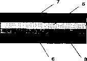
Fig. 1 is the cross sectional view of the siloxanes adhesive sheet of the present invention of production among the embodiment 2.
Fig. 2 is the cross sectional view of the siloxanes adhesive sheet of the present invention of embodiment 1 and embodiment 3-5 production.
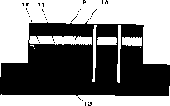
Fig. 3 relates to the cross sectional view of the part cut crystal produced among the embodiment 6 of semi-conductor chip of the present invention and chip connect elements adhering method.
Fig. 4 is the cross sectional view of the semiconducter device of the present invention produced among the embodiment 1-6.
Fig. 5 is the cross sectional view of the semiconducter device of the present invention of production among the embodiment 7.
Reference marker
1: argillaceous curable silicone compositions layer
2: argillaceous curable silicone compositions layer
3: protective membrane
4: protective membrane
5; The siloxanes cured layer
6: argillaceous curable silicone compositions layer
7: protective membrane
8: protective membrane
9: wafer
10: the siloxanes cured layer
11: argillaceous curable silicone compositions layer
12: protective membrane
13: adhesive sheet
14: semi-conductor chip
15: the siloxanes cured layer
16: the siloxanes cured layer
17: the semi-conductor chip connect elements
18: bonding wire
19: silicone rubber base bonding coat
Detailed description of preferred embodiments
The siloxanes adhesive sheet
Fig. 1 shows siloxanes adhesive sheet of the present invention.This sheet material has argillaceous curable silicone compositions layer 1 and have curing speed on opposite side and is slower than the argillaceous silicone composition layer 2 of mentioning for the first time layer on a side.The curing speed of these curable silicone compositions can be for example based on its 90% curing time { t
c(90) } come relatively, described 90% curing time is the regulation according to JIS K 6300, measures down at identical temperature condition (for example 130 ℃, 150 ℃) in the sulfuration test of using vibration sulfuration tester to carry out.Do not limit the poor of curing speed, but have the t of the curable silicone compositions of low curing speed
c(90) with t with curable silicone compositions of high curing rate
c(90) ratio is at 130 ℃ down preferred 5 times or bigger and more preferably 10 times or bigger, perhaps at 150 ℃ preferred down 2 times or bigger and more preferably 5 times or bigger.
The thickness of limit combination layer 1 not, but preferred 100 microns (μ m) or lower, more preferably 1-100 μ m and even more preferably 1-50 μ m.The also thickness of limit combination layer 2 not, but preferred 100 microns or lower, more preferably 1-100 μ m and even more preferably 1-50 μ m.Do not limit sheet thickness yet, but preferred 100 microns or lower.
Do not limit plasticity value as these argillaceous curable silicone compositions of JIS K 6249 regulation, and can be identical or different.Plasticity value is all preferably in the 100-800 scope and more preferably in the 100-700 scope and even more preferably in the 100-500 scope.Plasticity value is when according to the technical requirements of JIS K 6249, and by parallel plate plastometer (William ' sPlastimeter), { volume is 2 ± 0.02cm to apply the sample that loads to of 49 ± 0.05N
3Cylindrical object (diameter: 16mm, highly: 10mm) } numerical value during last 3 minute.
Not restricted passage is solidified these argillaceous curable silicone compositions and the performance of the curing silicone material that obtains, and can be identical or different.The curing silicone material preferably has elastomer performance, more preferably rubber performance.Do not limit the mechanism of solidifying these argillaceous curable silicone compositions and can be identical or different.The example of curable silicone compositions comprises the silicone composition of silicone composition, the condensation curable of hydrosilylation curable, by the curable silicone composition of the free radical reaction that comprises organo-peroxide with by the curable silicone composition of high-energy radiation.In siloxanes adhesive sheet of the present invention, the curable silicone compositions of the curable silicone compositions of slow curing speed and very fast curing speed is the silicone composition of preferred hydrosilylation curable all.
The silicone composition of these hydrosilylation curables preferably comprises the organopolysiloxane that (A) each molecule has at least two alkenyls; (B) filler; (C) each molecule has at least two organopolysiloxanes with the silicon bonded hydrogen atom; (D) adhesion promotor; (E) curable silicone compositions of hydrosilylation catalysts.
Component (A) is the organopolysiloxane that each molecule has at least two alkenyls.The weight average degree of polymerization preferred 3000 of component (A) or bigger and its performance be the performance of natural rubber preferably.The example of the molecular structure of component (A) comprises linear chain structure, branched structure and the reticulated structure of linear chain structure, part branching.The non-limiting examples of alkenyls of component (A) comprises vinyl, allyl group, butenyl, pentenyl and hexenyl, wherein preferred vinyl especially.The example of the bonding position of these alkenyls comprises the end position of molecular chain and/or the side chain of molecular chain.The examples of groups except alkenyl that is bonded on the Siliciumatom comprises replacement or unsubstituted univalence hydrocarbyl such as methyl, ethyl, propyl group, butyl, amyl group, hexyl, heptyl and other this alkyl; Phenyl, tolyl, xylyl, naphthyl and other this aryl; Benzyl, styroyl and other this aralkyl; Chloro methyl, 3-chloropropyl, 3,3,3-trifluoro propyl and other this haloalkyl, wherein especially preferable methyl, phenyl and similar group.When component (A) when containing phenyl, resulting sheet is endowed excellent lower temperature resistance and auxiliary down semi-conductor chip is bonded on the chip connect elements of this sheet material and the reliability of the semiconducter device that obtains can be improved.
Component (B) is a filler, and it reduces the flowability of above-mentioned composition and gives by solidifying the physical strength of the curing composition that above-mentioned composition obtains.Component (B) be can with the filler of curable silicone composition mixed together, only otherwise damage that purpose of the present invention gets final product and example comprises precipitated silica, pyrogenic silica, baked silica, titanium oxide, aluminum oxide, glass, quartz, silico-aluminate, ferric oxide, zinc oxide, lime carbonate, carbon black, silicon carbide, silicon nitride, boron nitride and other this mineral filler; By handling the mineral filler that these fillers obtain with organo-halogen-silane, organoalkoxysilane, organosilazanes and other this silicoorganic compound; Silicone resin, Resins, epoxy, fluoro-resin and other this resin micro mist; Filler and other this conductive metal powder such as silver, copper; With the silicone elastomer powder.The enhancing silicon-dioxide of especially preferred precipitated silica, pyrogenic silica and other type, and colloidal calcium carbonate, carbon black and other this thickening and toughness reinforcing particulate filler.
In above-mentioned composition, do not limit the content of component (B), but in per 100 parts by weight of component (A), preferably in 1-1000 weight part scope, more preferably in 5-800 weight part scope, even more preferably in 5-500 weight part scope, especially preferably in 5-200 weight part scope and ideally in 5-100 weight part scope.Especially, when using the particulate filler can give intensity during as component (B), in per 100 parts by weight of component (A), content is preferably in 1-100 weight part scope and more preferably in 1-50 weight part scope.This is that the gained cured product often can't be endowed enough physical strengths, surpasses going up in limited time of above-mentioned scope and work as content, often is difficult to prepare uniform composition because prescribe a time limit less than the following of above-mentioned scope when the content of component (B).
Component (C) is the linking agent in the above-mentioned composition and is to have at least two organopolysiloxanes with the silicon bonded hydrogen atom on each molecule.The example of the molecular structure of component (C) comprises linear chain structure, the linear chain structure of part branching, branched structure, ring structure and reticulated structure.In component (C), the example that is bonded to the bonding position of the hydrogen atom on the Siliciumatom comprises the side chain of the end position of molecular chain or molecular chain or these two.In component (C), be bonded to the examples of groups except hydrogen atom on the Siliciumatom and comprise and foregoing those identical replacements or unsubstituted univalence hydrocarbyl and especially preferable methyl and phenyl.Do not limit the viscosity of component (C) under 25 ℃, but be preferably 1-100000mPa.s and more preferably 1-10000mPa.s.
In said composition, do not limit the content of component (C), as long as its content is enough to solidify said composition, with in the every mol alkenyl in the component (A), in said composition with the silicon bonded hydrogen atom preferably in the 0.1-10mol scope, more preferably in the 0.1-5mol scope, even more preferably in the 0.5-5mol scope and ideally in the 1-5mol scope.This is that resulting composition tends to solidify insufficient and works as content and surpasses going up in limited time of above-mentioned scope because prescribe a time limit less than the following of above-mentioned scope when the content of component (C), and the thermotolerance of gained cured product is tended to decline.
Component (D) is to give composition satisfied fusible adhesion promotor.Component (D) preferably each molecule has at least one and is bonded to the silicoorganic compound of the hydrolysable group on the Siliciumatom and more preferably has at least two silicoorganic compound that are bonded to the hydrolysable group on the same Siliciumatom.This hydrolysable group can be for example methoxyl group, oxyethyl group, propoxy-, butoxy, methoxyl group-oxyethyl group, or other this alkoxyl group; Acetoxyl group or other this acyloxy; Different propenyloxy group or other this alkenyloxy; Or DMKO, methyl ethyl ketone oxime or other this oximido, but preferred alkoxyl group of hydrolysable group and more preferably methoxyl group.Component (D) preferably has the silicoorganic compound of trimethoxy.In these silicoorganic compound, except with foregoing those identical replacements or unsubstituted univalence hydrocarbyl, the examples of groups except hydrolysable group that is bonded on the Siliciumatom comprises 3-epoxypropoxy, 4-epoxy third oxygen-butyl and other this epoxy third oxyalkyl; 2-(3,4-epoxy group(ing) cyclohexyl) ethyl, 3-(3,4-epoxy group(ing) cyclohexyl) propyl group and other this epoxy group(ing) cyclohexyl alkyl; The unit price organic group that contains epoxy group(ing) is as 4-oxyranyl butyl, 8-oxyranyl octyl group and other this oxyranyl alkyl; 3-methacryloxypropyl and other this unit price organic group that contains acryl; And hydrogen atom.Owing to can provide satisfied bonding to various matrixes, preferred each molecule of these silicoorganic compound has the unit price organic group that at least one contains epoxy group(ing).The example of this silicoorganic compound comprises organosilane, organo-siloxane and silatranes.The example of the molecular structure of this organo-siloxane comprises linear chain structure, branched structure, ring structure and the reticulated structure of linear chain structure, part branching and especially preferred linear chain structure, branched structure or reticulated structure.
In component (D), the example of silicoorganic compound comprises 3-glycidoxy-propyltrimethoxy silane, 2-(3,4-epoxy group(ing) cyclohexyl) ethyl trimethoxy silane, 3-methacryloxypropyl trimethoxy silane and other this organosilane; Each molecule have with the silicon bonded alkoxy group and with the silicon bonded alkenyl or with the silicon bonded hydrogen atom in each at least one organo-siloxane, each molecule have the organosilane of at least one and silicon bonded alkoxy group or organo-siloxane and each molecule have with the hydroxyl of silicon bonding and with the silicon bonded alkenyl in each at least one the mixture of organo-siloxane; Organo-siloxane shown in following averaged unit formula:

A wherein, b and c are positive numbers,
Organo-siloxane shown in following averaged unit formula:
A wherein, b and c are positive numbers,
The silatranes that is shown below

The silatranes that is shown below
In said composition, do not limit the content of component (D), as long as it exists can give the satisfied fusible enough consumptions of composition, but in the component (A) of per 100 weight parts, preferably 0.01-20 weight part and more preferably 0.1-10 weight part.This is to prescribe a time limit less than the following of above-mentioned scope because work as the content of component (D), the binding property of resulting composition is tended to descend, and prescribe a time limit when content surpasses going up of above-mentioned scope, although the binding property of resulting composition remains unaffected, the mechanical features of gained cured product tends to be subjected to negative impact.
Component (E) is the hydrosilylation catalysts that promotes curing reaction in composition.The example of component (E) comprises platinum catalyst, rhodium catalyst and palladium catalyst and preferred platinum catalysts especially, because it can significantly promote curing reaction.The example of this platinum catalyst comprises fine powder, the platinum black of platinum, the fine silica powder of carrying platinum, gac, Platinic chloride, the alcoholic solution of Platinic chloride, platinum-alkene complex, the platinum alkenyl siloxanes complex compound of carrying platinum, and toner, wherein these platinum catalysts disperse or are encapsulated in acrylic resin, polycarbonate resin, silicone resin, polyamide resin or other this thermoplastic resin.
In said composition, do not limit the content of component (E), as long as it exists with the consumption of the curing reaction that is enough to promote above-mentioned composition; For example, when platinum catalyst when the component (E), the content of the platinum in catalyzer is with respect to preferred 0.01-1000ppm unit weight of composition and more preferably 0.1-500ppm.This is to prescribe a time limit less than the following of above-mentioned scope because work as the content of component (E), the curing reaction of resulting composition tends to extremely slow, and prescribe a time limit when content surpasses going up of above-mentioned scope, although it is unaffected substantially that curing speed still keeps, the gained cured product is in and is colored or experiences among the danger of other non-required variation.
In order to regulate curing speed, above-mentioned composition preferably contains curing inhibitors, as 3-methyl isophthalic acid-butine-3-alcohol, 3, and 5-dimethyl-1-hexin-3-alcohol, phenyl butynol, or another this alkynol; 3-methyl-pirylene, 3,5-dimethyl-3-hexene-1-alkynes or another this alkene-alkine compounds; 1,3,5,7-tetramethyl--1,3,5,7-tetrem thiazolinyl cyclotetrasiloxane, 1,3,5,7-tetramethyl--1,3,5,7-four hexenyl cyclotetrasiloxanes or contain another this organo-siloxane of alkenyl; Molecular formula CH
3Si[OC (CH
3)
2C ≡ CH]
3Shown organosilane, molecular formula CH
3(CH
2=CH) Si[OC (CH
3)
2C ≡ CH]
2Shown organosilane, molecular formula (CH
3)
3Si[OC (CH
3)
2C ≡ CH] shown in organosilane or contain another this organosilane of alkynyloxy group; Or benzotriazole.
In said composition, do not limit the content of curing inhibitors, but in per 100 parts by weight of component (A), preferred 0.00001-5 weight part.This is to prescribe a time limit less than the following of above-mentioned scope because work as the content of curing inhibitors, the curing speed of resulting composition is difficult to regulate and the processing operation suffers damage, and prescribe a time limit when content surpasses going up of above-mentioned scope, resulting composition is in and solidifies among the inadequate danger.
But composition also can contain dyestuff, pigment, gives stable on heating reagent, fire retardant and as other optional components mixed together other additive in the curable silicone compositions, only otherwise damaging purpose of the present invention gets final product.
Curing speed for the silicone composition of regulating any hydrosilylation curable of using of the above-mentioned sheet material of preparation, can for example select the type of component (C), select the type of component (E), regulate its content, select the type of curing inhibitors and regulate its content.Particularly, when in composition, when having organopolysiloxane with the silicon bonded hydrogen atom in the end position of molecular chain as component (C), realize higher reactivity, described higher level of reactivity is by having organopolysiloxane with the silicon bonded hydrogen atom and provide and therefore resulting composition fast setting in the side chain of molecular chain.In addition, in said composition, adopt the component (E) of big content, resulting composition solidifies more quickly.In addition, adopt the curing inhibitors of big content, resulting composition solidifies more slowly.Therefore, can prepare argillaceous curable silicone compositions with different curing speeds.The curing speed of these argillaceous curable silicone compositions can be for example based on its 90% curing time { t
c(90) } determine that described 90% curing time is the regulation according to JIS K6300, measure down at identical temperature condition (for example 130 ℃, 150 ℃) in the sulfuration test of using vibration sulfuration tester to carry out.
In Fig. 1, protective membrane 3 and 4 bonds on two surfaces of sheet material securely.The employing of protective membrane is chosen wantonly, but protective membrane preferably bonds on the either side or both sides of sheet material securely, because they avoid dust deposit on the front of sheet material.When using sheet material, peel off protective membrane.Protective membrane 3 can be identical or different with 4.The example of this protective membrane comprises the film that contains polyethylene terephthalate resin (PET), acrylic resin (PP), polyethersulfone resin (PES), cellulose triacetate resin (TAC) and other this celluosic resin and polyimide resin, vibrin, polyether resin, Resins, epoxy, resol, polyamide resin and other this organic resin particularly; Wherein contain the film that the surface of the film of these organic resins covers with fluorocarbon resin or another organic resin.
Do not limit the method for preparing sheet material, comprise wherein and will be applied on the protective membrane with example at the solution of the argillaceous curable silicone compositions in toluene, heptane or another this organic solvent, the organic solvent solution that curing speed is different from the argillaceous curable silicone compositions of foregoing is applied on another film and the method for lamination argillaceous curable silicone compositions together then similarly; Wherein be applied to the organic solvent solution of argillaceous curable silicone compositions on the protective membrane and further apply the method for organic solvent solution that curing speed is different from the argillaceous curable silicone compositions of foregoing; Wherein use the composition covered with protective film, apply the method for organic solvent solution that curing speed is different from the argillaceous curable silicone compositions of foregoing then by calendering.
Fig. 2 shows the present invention, and another can supply alternate siloxanes adhesive sheet.This sheet material has cured silicone layer 5 and have the curable silicone composition layer 6 of argillaceous on another surface on a surface.Do not limit the thickness of cured layer 5, but preferred 100 microns or lower, more preferably 1-100 micron and even more preferably 1-50 micron.The also thickness of limit combination layer 6 not, but preferred 100 microns or lower, more preferably 1-100 micron and even more preferably 1-50 micron.Do not limit the thickness of sheet material yet, but preferred 100 microns or lower.
For example the silicone composition of the silicone composition by solidifying hydrosilylation curable, condensation curable, by the curable silicone composition of the free radical reaction that comprises organo-peroxide, by the curable silicone composition of high-energy radiation, or another curable silicone composition forms cured layer 5, but preferably forms cured layer 5 by the silicone composition that solidifies hydrosilylation curable.Do not limit the performance of cured product, but preferably have elastomeric those performances and especially preferably have those performances of rubber.
In this sheet material, do not limit plasticity value, but preferred 100-800, more preferably 100-700 and even more preferably 100-500 as the argillaceous curable silicone compositions of JIS K 6249 regulation.According to the technical requirements of JIS K 6249, this plasticity value is when by parallel plate plastometer (William ' s Plastimeter), and { volume is 2 ± 0.02cm to apply the sample that loads to of 49 ± 0.05N
3Cylindrical object (diameter: 16mm, highly: 10mm) } numerical value during last 3 minute.
Not restricted passage is solidified the argillaceous curable silicone compositions and the performance of the curing silicone compositions that obtains, but preferably has elastomeric those performances and especially preferably have those performances of rubber.Do not limit the consolidated structures of this curable silicone compositions, comprise the silicone composition of silicone composition, the condensation curable of hydrosilylation curable with the example, by the curable silicone composition of the free radical reaction that comprises organo-peroxide, with by the curable silicone composition of high-energy radiation, the silicone composition of especially preferred hydrosilylation curable wherein.The silicone composition of hydrosilylation curable as previously mentioned.
In Fig. 2, protective membrane 7 and 8 bonds on two surfaces of siloxanes adhesive sheet securely.The employing of these protective membranes is chosen wantonly, but protective membrane preferably bonds on the either side or both sides of sheet material securely, because they avoid dust deposit on the front of sheet material.When using sheet material, peel off protective membrane.Protective membrane 7 can be identical or different with 8.The example of this protective membrane comprises film as hereinbefore.
Do not limit the method for preparing sheet material, comprise wherein and will be applied on the protective membrane with example at the solution of the argillaceous curable silicone compositions in toluene, heptane or another this organic solvent, the organic solvent solution that curing speed is different from the argillaceous curable silicone compositions of foregoing is applied on another film similarly, the lamination argillaceous curable silicone compositions and the method for only solidifying the one deck in the argillaceous curable silicone compositions together then; Wherein the organic solvent solution of argillaceous curable silicone compositions is applied on the protective membrane and solidifies said composition, the method for the organic solvent solution that applies the argillaceous curable silicone compositions then to the cured product; Wherein apply the liquid curable silicone composition to protective membrane, solidify said composition, to be applied on another protective membrane at the solution of the argillaceous curable silicone compositions in toluene, heptane or another this organic solvent then and the method for these films of lamination together; Wherein component (C) or component (E) are applied on the protective membrane, the organic solvent solution of argillaceous curable silicone compositions is applied on another protective membrane similarly, component (C) or component (E) with argillaceous curable silicone compositions lamination, are only solidified the method on a surface of argillaceous curable silicone compositions then; Wherein use the curable silicone compositions covered with protective film, the method for the organic solvent solution that applies the argillaceous curable silicone compositions then to the cured product by calendering.
This siloxanes adhesive sheet of the present invention is suitable for use as the adhesive sheet of all types matrix, because it can bonding satisfactorily smooth matrix and has the matrix of degree of irregularity from the teeth outwards and can make the thickness of adhesive linkage almost become even.Especially, using siloxanes adhesive sheet of the present invention is favourable as chip connect elements and the tackiness agent that has the semi-conductor chip of degree of irregularity at least one surface, because can make the thickness of adhesive linkage become almost even, therefore in wiring technique for sticking process subsequently, can not produce inconvenience.This siloxanes adhesive sheet of the present invention is suitable as tackiness agent, is used for the semi-conductor chip that has degree of irregularity at least one surface is bonded to the chip connect elements.Sheet material preferably has the uranium and the thorium of low levels.Sheet material also preferably has sodium, potassium and other this alkalimetal ion or the halide-ions of low levels.In addition, sheet material preferably has the low molecular weight polyorganosiloxane of low levels.
The method of bonding semi-conductor chip and chip connect elements
Fig. 3 shows the method for bonding semi-conductor chip of the present invention and chip connect elements.The method comprising the steps of:
(1) by layered product is cut into small pieces, produce semi-conductor chip, wherein said layered product by bond to curing silicone layer 10 on the wafer 9, securely bond to argillaceous curable silicone compositions layer 11 on the cured layer 10, bond to the protective membrane 12 on the composition layer 11 and form securely with the sheet material 13 that tackiness agent is connected on the film 12;
(2) from chip, peel off protective membrane 12 and sheet material 13;
(3) by suppressing semi-conductor chips to the chip connect elements, semi-conductor chip is bonded on the chip connect elements by composition layer 11; With
(4) solidify said composition layer 11.
The example that forms the method for layered product (described layered product comprises the cured silicone layer 10 that bonds on the wafer 9 and bonds to argillaceous curable silicone compositions layer 11 on the cured layer 10 securely) comprises, the layer of curing composition in layered product (I), so that prevent the layer solidified method of composition (II), wherein said layered product comprises the layer of the argillaceous curable silicone compositions (I) that bonds to securely on the wafer and bonds to the layer that the argillaceous curable silicone compositions (II) of the layer curing speed that is lower than composition (I) was gone up and given to composition (I) securely; Wherein the cured product layer with the curing silicone material bonds on the wafer, so that prevent argillaceous curable silicone compositions solidified method, described cured product layer forms by lamination solidified silicone material layer and the argillaceous curable silicone compositions layer that bonds to securely on the cured product on the wafer.The siloxanes adhesive sheet that uses in these methods as previously mentioned.
Next, adhesive sheet 13 is laminated on the protective membrane 12 and from wafer 9 sides cuts into small pieces.Can cut adhesive sheet 13 then locates in the middle of almost.Can be by from the semi-conductor chip of acquisition like this, peeling off protective membrane 12 and adhesive sheet 13; by argillaceous curable silicone compositions layer 11; under pressure with die bonding to the semi-conductor chip connect elements; the curing composition layer 11 then, thus bonding semi-conductor chip and chip connect elements.Be not specially limited bonding condition, but preference is as being heated to 50-250 ℃ and more preferably be heated to 100-150 ℃.Suppress preferred 1 second-2 hours bonding time.Be not specially limited pressure, as long as semi-conductor chip or chip connect elements are not damaged, but preferably in the 0.3-2.0MPa scope.
Semiconducter device
In semiconducter device of the present invention, by above-mentioned siloxanes adhesive sheet, semi-conductor chip is bonded on the chip connect elements, comprise diode, transistor, thyristor, monolithic integrated circuit (IC) with the example of semiconducter device, mix IC, large-scale integrated circuit (LSI) and very large-scale integrated circuit (VLSI) and the packaged piece that is called chip scale package (CSP) are also included within the semiconducter device of the present invention.The example of semi-conductor chip comprises diode, transistor, thyristor, monolithic IC and semi-conductor chip and this semi-conductor chip circuit board component mounted thereto, as mixing IC, LSI and VLSI.
The example of semi-conductor chip connect elements comprises pottery, glass, Resins, epoxy, polyimide resin, resol, Bakelite resin, melamine resin, glass fibre enhanced Resins, epoxy, glass fibre enhanced BT resin and other sort circuit plate and chip carrier and joint.The example of bonding wire comprises gold and silver, aluminium and other this metal foil line.The ultrasonic thermocompression bonding method that connects bonding wire that is commonly used for that contracts.
The example of semiconducter device comprises the semiconducter device that contains the siloxanes adhesive sheet, described siloxanes adhesive sheet has the layer of argillaceous curable silicone compositions (I) on a side, with on opposite side, have curing speed be slower than composition (I) the layer argillaceous curable silicone compositions (II) the layer, thereby when semi-conductor chip bonds on the chip connect elements, (i) layer of composition (I) so solidifies, so that keep with when semi-conductor chip contacts at the layer of composition (I), the layer of composition (II) is still uncured, keep layer curing with composition (II) when the semi-conductor chip connect elements contact at the layer of composition (II) subsequently, or thereby (ii) the layer of composition (I) so solidifies, so that keep layer still uncured with composition (II) when the semi-conductor chip connect elements contacts at the layer of composition (I), keep with when semi-conductor chip contacts layer solidified semiconducter device of composition (II) subsequently at the layer of composition (II).
Be not specially limited the siloxanes adhesive sheet is bonded to condition on semi-conductor chip or the chip connect elements, but for example preferably under 100-150 ℃, heating under 50-250 ℃ and more preferably.Suppress preferred 1 second-2 hours bonding time.Be not specially limited pressure, as long as semi-conductor chip or chip connect elements are not damaged, but preferred 0.3-2.0MPa.
In semiconducter device according to above-mentioned (i), bond to the layer of argillaceous curable silicone compositions (I) on the semi-conductor chip and the surface of semi-conductor chip can or smooth or irregular.Under above-mentioned bonding condition, the layer of argillaceous curable silicone compositions (II) solidifies cured product layer (I) under the solidified condition therein.Argillaceous curable silicone compositions (II) the layer bond on the semi-conductor chip connect elements then and the surface of connect elements can or smooth or irregular.Next, can be by under above-mentioned bonding condition, solidifying, thus the layer of bonding composition (II).
In according to above-mentioned semiconducter device (ii), with argillaceous curable silicone compositions (I) the layer bond on the semi-conductor chip connect elements and the surface of chip connect elements can or smooth or irregular.Under above-mentioned bonding condition, the layer of argillaceous curable silicone compositions (II) solidifies cured product layer (I) under the solidified condition therein.Argillaceous curable silicone compositions (II) the layer bond on the semi-conductor chip connect elements then and the surface of connect elements can or smooth or irregular.Next, can be by under above-mentioned bonding condition, solidifying, thus the layer of bonding composition (II).
Wherein the example that is used to this semiconducter device of bonding semi-conductor chip to the chip connect elements at the siloxanes adhesive sheet that has the curing silicone layer on the side and have argillaceous curable silicone compositions layer on the opposite side comprises: bonding cured layer (iii) wherein like this, so that keep still uncured with composition layer when semi-conductor chip contacts at cured layer, keep semiconducter device with curing composition layer when the semi-conductor chip connect elements contacts at composition layer subsequently, bonding cured layer perhaps (iv) wherein like this, so that keep still uncured, with subsequently at the semiconducter device of composition layer maintenance with curing composition layer when semi-conductor chip contacts with composition layer when the semi-conductor chip connect elements contacts at cured layer.
Be not specially limited the siloxanes adhesive sheet is bonded to condition on semi-conductor chip or the chip connect elements, but for example preferably 50-250 ℃ of heating and more preferably 100-150 ℃ of heating down down.Compacting is sticking by preferred 1 second-2 hours time.Be not specially limited pressure, as long as semi-conductor chip or chip connect elements are not damaged, but preferably in the 0.3-2.0MPa scope.
Especially, in above-mentioned (iii) semiconducter device, semi-conductor chip must have slick surface, because the siloxanes cured layer is bonded on the semi-conductor chip, with under above-mentioned bonding condition, argillaceous curable silicone compositions layer bonding cured layer under the solidified condition not therein.Bond to argillaceous curable silicone compositions layer on the semi-conductor chip connect elements then and the surface of chip connect elements preferably has degree of irregularity.Next, by under above-mentioned bonding condition, solidifying, thus bonding composition.
In above-mentioned (iv) semiconducter device, the chip connect elements must have slick surface, because the siloxanes cured layer is bonded on the semi-conductor chip connect elements, with under above-mentioned bonding condition, argillaceous curable silicone compositions layer bonding cured layer under the solidified condition not therein.Bond to argillaceous curable silicone compositions layer on the semi-conductor chip then and the surface of chip preferably has degree of irregularity.Next, by under above-mentioned bonding condition, solidifying, thus bonding composition.
Embodiment
In an embodiment, viscosity is the numerical value under 25 ℃.The plasticity value of argillaceous curable silicone compositions is the technical requirements according to JIS K 6249, and by parallel plate plastometer (William ' s Plastimeter), { volume is 2 ± 0.02cm to apply the sample that loads to of 49 ± 0.05N
3Cylindrical object (diameter: 16mm, highly: 10mm) } numerical value during last 3 minute.The curing speed of argillaceous curable silicone compositions is based on its 90% curing time { t
c(90) } represent that described 90% curing time is the regulation according to JIS K 6300, measure down at identical temperature condition (for example 130 ℃, 150 ℃) in the sulfuration test of using vibration sulfuration tester to carry out.In addition, according to the regulation of JIS K 6253, by the hardness of A type hardness tester instrumentation amount curing silicone material.
The preparation of reference example 1-argillaceous rubber composition I
Adopt kneader, by heating and the two ends of mixing 100 weight parts (weight-average molecular weight=370000) molecular chain with the end capped dimethyl siloxane of dimethylvinylsiloxy/methyl ethylene silicone copolymers untreated rubber (it comprises 99.85mol% dimethyl siloxane units and 0.15mol% methyl vinyl siloxane unit), 10.0 weight part viscosity is the two ends end capped dimethyl siloxane oligopolymer of silanol group of the molecular chain of 60mPa.s, with 40 weight part pyrogenic silicas (AEROSIL 200 , by Japan Aerosil, Co., Ltd. makes; BET specific surface area 200m
2/ g), produce silicone rubber based matter.
Next, use the two-roller mill machine, the described silicon rubber matrix of uniform mixing 100 weight parts, 0.8 weight part viscosity are that the two ends of molecular chain of 30mPa.s are with the end capped hydrogenated methyl polysiloxane of trimethylsiloxy (in the hydrogenated methyl polysiloxane be 3.1mol/mol at the two ends of molecular chain with dimethylvinylsiloxy end-blocking with silicon bonded hydrogen atom content and be included in vinyl in dimethyl siloxane/methyl ethylene silicone copolymers untreated rubber in the above-mentioned silicon rubber matrix), 0.05 weight part formula CH
3Si[OC (CH
3)
2C ≡ CH]
3Shown organosilane as curing inhibitors and 1.0 weight parts by the organo-siloxane shown in the following averaged unit formula as adhesion promotor;

Mix 1 of platinum then, 1 of 3-divinyl tetramethyl disiloxane complex compound, 3-divinyl tetramethyl disiloxane solution (in composition of the present invention, the metal platinum content in complex compound is the 20ppm weight unit) is produced argillaceous rubber composition (I).
The plasticity value of this argillaceous curable silicone compositions (I) is 240.According to the regulation of JIS K 6300, the curing speed t of this argillaceous curable silicone compositions (I)
c(90) be 2.5 minutes under 130 ℃ and be 1 minute under 150 ℃.Hardness by the silicon rubber that solidify to obtain is 60.
Next, stir 20 weight parts these argillaceous rubber composition (I) and 80 parts by weight of toluene in the flask that separates, producing viscosity is the toluene solution of the argillaceous rubber composition (I) of 3500mPa.s.
The preparation of reference example 2-argillaceous rubber composition II
Adopt kneader, by heating and the two ends of mixing 100 weight parts (weight-average molecular weight=370000) molecular chain with the end capped dimethyl siloxane of dimethylvinylsiloxy/methyl ethylene silicone copolymers untreated rubber (it comprises 99.85mol% dimethyl siloxane units and 0.15mol% methyl vinyl siloxane unit), 10.0 weight part viscosity is the two ends end capped dimethyl siloxane oligopolymer of silanol group of the molecular chain of 60mPa.s, with 40 weight part pyrogenic silicas (AEROSIL 200 , by Japan Aerosil, Co., Ltd. makes; BET specific surface area 200m
2/ g), produce silicone rubber based matter.
Next, use the two-roller mill machine, the above-mentioned silicon rubber matrix of uniform mixing 100 weight parts, 0.8 weight part viscosity are that the two ends of molecular chain of 30mPa.s are with the end capped hydrogenated methyl polysiloxane of trimethylsiloxy (in this hydrogenated methyl polysiloxane be 3.1mol/mol at the two ends of molecular chain with dimethylvinylsiloxy end-blocking with silicon bonded hydrogen atom content and be included in vinyl in dimethyl siloxane/methyl ethylene silicone copolymers untreated rubber in the above-mentioned silicon rubber matrix), 0.2 weight part molecular formula CH
3Si[OC (CH
3)
2C ≡ CH]
3Shown organosilane as curing inhibitors and 1.0 weight parts by the organo-siloxane shown in the following averaged unit formula as adhesion promotor;

Mix 1 of platinum then, 1 of 3-divinyl tetramethyl disiloxane complex compound, 3-divinyl tetramethyl disiloxane solution (in composition of the present invention, the metal platinum content in complex compound is the 20ppm weight unit) is produced argillaceous rubber composition (II).
The plasticity value of argillaceous rubber composition (II) is 240.According to the regulation of JIS K 6300, the curing speed t of argillaceous rubber composition (II)
c(90) be 40 minutes under 130 ℃ and be 10 minutes under 150 ℃.Hardness by the silicon rubber that solidify to obtain is 60.
Next, stir above-mentioned argillaceous rubber compositions of 20 weight parts (II) and 80 parts by weight of toluene in the flask that separates, producing viscosity is the toluene solution of the argillaceous rubber composition (II) of 3500mPa.s.
The preparation of reference example 3-argillaceous rubber composition III
Adopt kneader, by heating and the two ends of mixing 100 weight parts (weight-average molecular weight=370000) molecular chain with the end capped dimethyl siloxane of dimethylvinylsiloxy/methyl ethylene silicone copolymers untreated rubber (it comprises 99.85mol% dimethyl siloxane units and 0.15mol% methyl vinyl siloxane unit), 10.0 weight part viscosity is the two ends end capped dimethyl siloxane oligopolymer of silanol group of the molecular chain of 60mPa.s, with 40 weight part pyrogenic silicas (AEROSIL 200 , by Japan Aerosil, Co., Ltd. makes; BET specific surface area 200m
2/ g), produce silicone rubber based matter.
Next, use the two-roller mill machine; This silicon rubber matrix of uniform mixing 100 weight parts, 0.8 weight part viscosity are that the two ends of molecular chain of 30mPa.s are with the end capped hydrogenated methyl polysiloxane of trimethylsiloxy (in the hydrogenated methyl polysiloxane be 3.1mol/mol at the two ends of molecular chain with dimethylvinylsiloxy end-blocking with silicon bonded hydrogen atom content and be included in vinyl in dimethyl siloxane/methyl ethylene silicone copolymers untreated rubber in the above-mentioned silicon rubber matrix), 0.2 weight part molecular formula CH
3Si[OC (CH
3)
2C ≡ CH]
3Shown organosilane as curing inhibitors and 1.0 weight parts by the organo-siloxane shown in the following averaged unit formula as adhesion promotor;

Mix 1 of platinum then, 1 of 3-divinyl tetramethyl disiloxane complex compound, 3-divinyl tetramethyl disiloxane solution (in composition of the present invention, the metal platinum content in complex compound is the 20ppm weight unit) is produced argillaceous rubber composition (II).
The plasticity value of this argillaceous rubber composition (III) is 240.According to the regulation of JIS K 6300, the curing speed t of this argillaceous rubber composition (III)
c(90) be 40 minutes under 130 ℃ and be 10 minutes under 150 ℃.Hardness by the silicon rubber that solidify to obtain is 60.
Next, stir above-mentioned argillaceous rubber compositions of 20 weight parts (III) and 80 parts by weight of toluene in the flask that separates, producing viscosity is the toluene solution of the argillaceous rubber composition (III) of 3500mPa.s.
Embodiment 1
By using scraper, the toluene solution that with thickness is the argillaceous rubber composition (II) produced in 25 microns the reference example 2 is applied on the polyester sulfone resin molding, at room temperature dry up 2 hours then, with by 150 ℃ down the heating gains solidified argillaceous siloxanes rubber composition (II) in 30 minutes, be 5 microns silicon rubber sheet material thereby produce the thickness that bonds to securely on the polyester sulfone resin molding.
Next, use scraper, be that the toluene solution of the argillaceous rubber composition (II) produced in 225 microns the reference example 2 is applied on the silicon rubber sheet material with thickness, and at room temperature dried up products therefrom 2 hours.The total thickness of silicon rubber sheet material that dries up and argillaceous rubber composition layer is 50 microns.Next; pass through rubber rollers; the polyester sulfone resin molding is bonded to securely on the surface of argillaceous rubber composition layer; silastic-layer and the argillaceous rubber composition layer shown in Figure 2 with lamination, production wherein bonds to two lip-deep siloxanes adhesive sheet securely as the polyester sulfone resin molding of protective membrane.
The siloxanes adhesive sheet is cut into the square of 10mm in a side, peel off the polyester sulfone resin molding that bonds to securely on the silastic-layer, compacting is bonded in 1 second of silicon of the 10mm of a side under the compacting of 190 ℃ and 1.0MPa, peel off the polyester sulfone resin molding that bonds to securely on the argillaceous rubber composition layer, bonding this layer of compacting is 20 microns to degree of irregularity under the compacting of 190 ℃ and 1.0MPa, on the wiring surface of the plate of making by glass fibre enhanced Resins, epoxy through 1 second, with at 150 ℃ of following heating gains 60 minutes, the argillaceous rubber composition is solidified, thereby produce device.
Measure the total thickness of this device, with thickness by the plate that deducts silicon and make by glass fibre enhanced Resins, epoxy, measurement is at the thickness of the place, four angles of chip siloxanes bonding coat, so find that the thickness of siloxanes bonding coat evenly is 48 microns in all cases.Upwards the tractive silicon experiences cohesive failure to confirm binding property and discovery siloxanes bonding coat, thereby confirms that binding property is satisfactory.
Next, it is bonding to contract by ultrasonic thermocompression, is that 30 microns metal wire bonds on the above-mentioned device with diameter, produces semiconducter device shown in Figure 4.30 these semiconducter device were left standstill under-50 ℃ 30 minutes, carry out thermal cycling test then immediately, wherein leaving standstill 30 minutes under 150 ℃ is 1 circulation and the defect conduction mark (conductive fraction defective) of estimating above-mentioned device.The results are shown in Table 1.
Embodiment 2
Use scraper, the toluene solution of the argillaceous rubber composition (I) that reference example 1 is produced is applied to 50 microns thickness and is different from the above-mentioned polyester sulfone resin molding and at room temperature dries up 2 hours.After drying, the thickness of the layer of argillaceous rubber composition (I) is 5 microns.
Use scraper, the toluene solution of the argillaceous rubber composition (II) that reference example 2 is produced is applied to 225 microns thickness and is different from the above-mentioned polyester sulfone resin molding and at room temperature dries up 2 hours.After drying, the thickness of the layer of argillaceous rubber composition (II) is 45 microns.
Next, the layer and the layer of argillaceous rubber composition (II) of lamination argillaceous rubber composition (I) together, produce siloxanes adhesive sheet shown in Figure 1, it comprises that the polyester sulfone resin molding bonds to two lip-deep two-layer argillaceous rubber composition.
The siloxanes adhesive sheet is cut into the square of 10mm in a side, peel off the polyester sulfone resin molding on the layer that bonds to argillaceous rubber composition (I) securely, be bonded in the siloxanes chip 2 minutes of the 10mm of a side by compacting under the pressure of 150 ℃ and 1.0MPa, solidify the layer of argillaceous rubber composition (I), peel off the polyester sulfone resin molding on the layer that bonds to argillaceous rubber composition (II) securely then, bonding this layer of compacting is 20 microns to degree of irregularity under the pressure of 190 ℃ and 1.0MPa, on the wiring surface of the plate of making by glass fibre enhanced Resins, epoxy through 1 second, with at 150 ℃ of following heating gains 60 minutes, so that the curing of argillaceous rubber composition, thereby produce device.
Measure the total thickness of this device, with thickness by the plate that deducts chip and make by glass fibre enhanced Resins, epoxy, measurement is at the thickness of the place, four angles of chip siloxanes bonding coat, so find that the thickness of siloxanes bonding coat evenly is 48 microns in all cases.Upwards tractive siloxanes chip experiences cohesive failure to confirm binding property and discovery siloxanes bonding coat, thereby confirms that binding property is satisfactory.
Next, it is bonding to contract by ultrasonic thermocompression, is that 30 microns metal wire bonds on the above-mentioned device with diameter, produces semiconducter device shown in Figure 4.30 these semiconducter device were left standstill under-50 ℃ 30 minutes, carry out thermal cycling test then immediately, wherein leaving standstill 30 minutes under 150 ℃ is 1 circulation and the defect conduction mark of estimating above-mentioned device.The results are shown in Table 1.
Embodiment 3
By the siloxanes adhesive sheet produced among the heating embodiment 2 down at 130 ℃ 10 minutes; solidify the only layer of argillaceous rubber composition (I); thereby produce siloxanes adhesive sheet shown in Figure 2; the layer of lamination silastic-layer and argillaceous rubber composition (II) wherein, and the polyester sulfone resin molding bonded on two surfaces securely as protective membrane.
The siloxanes adhesive sheet is cut into the square of 10mm in a side, peel off the polyester sulfone resin molding that bonds to securely on the silastic-layer, be bonded in the siloxanes chip 1 second of the 10mm of a side by binder under the pressure of 190 ℃ and 1.0MPa, peel off the polyester sulfone resin molding on the layer that bonds to argillaceous rubber composition (II) securely then, bonding this layer of compacting is 20 microns to degree of irregularity under the pressure of 190 ℃ and 1.0MPa, on the wiring surface of the plate of making by glass fibre enhanced Resins, epoxy through 1 second, with at 150 ℃ of following heating gains 60 minutes, the layer of argillaceous rubber composition (II) is solidified, thereby produce device.
Measure the total thickness of this device, with thickness by the plate that deducts chip and make by glass fibre enhanced Resins, epoxy, measurement is at the thickness of the place, four angles of chip siloxanes bonding coat, so find that the thickness of siloxanes bonding coat evenly is 48 microns in all cases.Upwards tractive siloxanes chip experiences cohesive failure to confirm binding property and discovery siloxanes bonding coat, thereby confirms that binding property is satisfactory.
Next, it is bonding to contract by ultrasonic thermocompression, is that 30 microns metal wire bonds on the above-mentioned device with diameter, produces semiconducter device shown in Figure 4.30 these semiconducter device were left standstill under-50 ℃ 30 minutes, carry out thermal cycling test then immediately, wherein leaving standstill 30 minutes under 150 ℃ is 1 circulation and the defect conduction mark of estimating above-mentioned device.The results are shown in Table 1.
Embodiment 4
Use gauze, at thickness be on 50 microns the polyester sulfone resin molding coating platinum 1, the toluene solution of 3-divinyl tetramethyl disiloxane complex compound (wherein in the weight unit of metal platinum, content is 500ppm) and gains were left standstill 2 hours and dry up.
Use scraper, the toluene solution of the argillaceous rubber composition (II) that reference example 2 is produced is applied on the polyester sulfone resin molding with 250 microns thickness and at room temperature dried up gains 2 hours.After drying, the thickness of the layer of argillaceous rubber composition (II) is 50 microns.
Next; the layer of lamination argillaceous rubber composition (II) and be coated with 1 of platinum together; the surface of 3-divinyl tetramethyl disiloxane complex compound; produce the argillaceous siloxanes adhesive sheet that the polyester sulfone resin molding bonds to two lip-deep argillaceous shape rubber composition securely; then by heating gains 10 minutes down at 130 ℃; only solidify and 1 of platinum; the surface of the layer of the argillaceous rubber composition (II) of 3-divinyl tetramethyl disiloxane complex compound contact; with lamination silastic-layer and argillaceous rubber composition layer, producing wherein, the polyester sulfone resin molding bonds to two lip-deep argillaceous siloxanes adhesive sheets securely as protective membrane.In argillaceous layer one side, siloxane layer is kept about 30 microns thickness.
Argillaceous siloxanes adhesive sheet is cut into the square of 10mm in a side, peel off the polyester sulfone resin molding that bonds to securely on the silastic-layer, be bonded in the siloxanes chip 1 second of the 10mm of a side by compacting under the pressure of 190 ℃ and 1.0MPa, peel off the polyester sulfone resin molding on the layer that bonds to argillaceous rubber composition (II) securely then, bonding this layer of compacting is 20 microns to degree of irregularity under the pressure of 190 ℃ and 1.0MPa, on the wiring surface of the plate of making by glass fibre enhanced Resins, epoxy through 1 second, with at 150 ℃ of following heating gains 60 minutes, the layer of argillaceous rubber composition (II) is solidified, thereby produce device.
Measure the total thickness of this device, with thickness by the plate that deducts chip and make by glass fibre enhanced Resins, epoxy, measurement is at the thickness of the place, four angles of chip siloxanes bonding coat, so find that the thickness of siloxanes bonding coat evenly is 48 microns in all cases.Upwards tractive siloxanes chip experiences cohesive failure to confirm binding property and discovery siloxanes bonding coat, thereby confirms that binding property is satisfactory.
Next, it is bonding to contract by ultrasonic thermocompression, is that 30 microns metal wire bonds on the above-mentioned device with diameter, produces semiconducter device.30 these semiconducter device were left standstill under-50 ℃ 30 minutes, carry out thermal cycling test then immediately, wherein leaving standstill 30 minutes under 150 ℃ is 1 circulation and the defect conduction mark of estimating above-mentioned device.The results are shown in Table 1.
Using gauze, is coating averaging unit molecular formula [(CH on 50 microns the polyester sulfone resin molding at thickness
3)
2HSiO
1/2]
0.6(SiO
2)
0.4Shown organopolysiloxane is (with the toluene solution (solid 10wt%) of silicon bonded hydrogen atom content=0.97wt%) with gains were left standstill 2 hours and dry up.
Use scraper, the toluene solution of the argillaceous rubber composition (II) that reference example 2 is produced is applied on the polyester sulfone resin molding with 250 microns thickness and at room temperature dried up products therefrom 2 hours.After drying, the thickness of the layer of argillaceous rubber composition (II) is 50 microns.
Next, the layer of lamination argillaceous rubber composition (II) and be coated with averaging unit molecular formula [(CH together
3)
2HSiO
1/2]
0.6(SiO
2)
0.4The surface of shown organopolysiloxane, produce the polyester sulfone resin molding bonds to the argillaceous shape rubber composition on it securely in both sides siloxanes adhesive sheet, by heating gains 10 minutes down, only solidify and averaging unit molecular formula [(CH then at 130 ℃
3)
2HSiO
1/2]
0.6(SiO
2)
0.4The surface of the layer of the argillaceous rubber composition (II) of shown organopolysiloxane contact; as shown in Figure 2; lamination silastic-layer and argillaceous rubber composition layer, producing wherein, the polyester sulfone resin molding bonds to two lip-deep argillaceous siloxanes adhesive sheet securely as protective membrane.In argillaceous layer one side, siloxane layer is kept about 30 microns thickness.
Argillaceous siloxanes adhesive sheet is cut into the square of 10mm in a side, peel off the polyester sulfone resin molding that bonds to securely on the silastic-layer, be bonded in the siloxanes chip 1 second of the 10mm of a side by compacting under the pressure of 190 ℃ and 1.0MPa, peel off the polyester sulfone resin molding on the layer that bonds to argillaceous rubber composition (II) securely then, bonding this layer of compacting is 20 microns to degree of irregularity under the pressure of 190 ℃ and 1.0MPa, on the wiring surface of the plate of making by glass fibre enhanced Resins, epoxy through 1 second, with at 150 ℃ of following heating gains 60 minutes, the layer of argillaceous rubber composition (II) is solidified, thereby produce device.
Measure the total thickness of this device, with thickness by the plate that deducts chip and make by glass fibre enhanced Resins, epoxy, measurement is at the thickness of the place, four angles of chip siloxanes bonding coat, so find that the thickness of siloxanes bonding coat evenly is 48 microns in all cases.Upwards tractive siloxanes chip experiences cohesive failure to confirm binding property and discovery siloxanes bonding coat, thereby confirms that binding property is satisfactory.
Next, it is bonding to contract by ultrasonic thermocompression, is that 30 microns metal wire bonds on the above-mentioned device with diameter, produces semiconducter device.30 these semiconducter device were left standstill under-50 ℃ 30 minutes, carry out thermal cycling test then immediately, wherein leaving standstill 30 minutes under 150 ℃ is 1 circulation and the defect conduction mark of estimating above-mentioned device.The results are shown in Table 1.
(wherein argillaceous rubber composition layer (I) and argillaceous rubber composition (II's) is pressed together layer by layer to peel off the siloxanes adhesive sheet; and protective layer is closely bonded on two surfaces) the protective membrane (in embodiment 2 produce) on the layer of argillaceous rubber composition (I), and before cutting into small pieces, use rubber rollers securely it to be bonded on 4 inches the silicon wafer.Next, heat gains 10 minutes down and solidify the only layer of argillaceous rubber composition (I) at 130 ℃.
Next; with thickness is that 90 microns adhesive sheet is laminated on the protective membrane that bonds to the siloxanes adhesive sheet securely; and described siloxanes adhesive sheet itself is bonded on the silicon wafer; slitting saw DAD 340 with using by Disco Corporation manufacturing cuts into the 10mm square with this product in a side.Cut away the basal surface of adhesive sheet, thereby stay 60 microns.
When using the semi-conductor chip of adhesive sheet adhesion cutting, protective membrane remains on the adhesive sheet side.By wherein at room temperature, under the pressure of 1.0MPa, on the wiring surface of the plate that to bond to degree of irregularity through compacting in 1 second be 20 microns with bonding to siloxanes adhesive sheet on the semi-conductor chip, made by glass fibre enhanced Resins, epoxy, with at 150 ℃ of following heating gains 60 minutes, make argillaceous rubber composition layer solidified method, thereby produce device.
Measure the total thickness of this device, with thickness by the plate that deducts chip and make by glass fibre enhanced Resins, epoxy, measurement is at the thickness of the place, four angles of chip siloxanes bonding coat, so find that the thickness of siloxanes bonding coat evenly is 48 microns in all cases.Upwards tractive siloxanes chip experiences cohesive failure to confirm binding property and discovery siloxanes bonding coat, thereby confirms that binding property is satisfactory.
Next, it is bonding to contract by ultrasonic thermocompression, is that 30 microns metal wire bonds on the above-mentioned device with diameter, produces semiconducter device shown in Figure 4.30 these semiconducter device were left standstill under-50 ℃ 30 minutes, carry out thermal cycling test then immediately, wherein leaving standstill 30 minutes under 150 ℃ is 1 circulation and the defect conduction mark of estimating above-mentioned device.The results are shown in Table 1.
Comparative Examples 1
At room temperature, by the Ross mixing machine, the two ends of molecular chain of mixing 72 weight part viscosity and be 40000mPa.s are with the end capped dimethyl polysiloxane of dimethylvinylsiloxy (contents of ethylene=0.08wt%), 15 weight part viscosity are that the two ends of molecular chain of 6000mPa.s are with dimethylvinylsiloxy end capped dimethyl siloxane/methyl ethylene silicone copolymers (contents of ethylene=0.84wt%), 1.5 weight parts water, 3 weight part hexamethyldisilazanes and 10 weight part pyrogenic silicas (AEROSIL 200 , by JapanAerosil, Co., Ltd. makes; BET specific surface area 200m
2/ g) 1 hour, decompression is heated and was mixed 2 hours under 170 ℃ then.With the products therefrom cool to room temperature, produce translucent pasty state silicon rubber matrix.
Next, the above-mentioned silicon rubber matrix of uniform mixing 100 weight parts, 3 weight part viscosity be 5mPa.s molecular chain two ends with the end capped dimethyl siloxane of trimethylsiloxy/hydrogenated methyl silicone copolymers (with the content of silicon bonded hydrogen atom=0.7wt%) (the two ends of molecular chain with trimethylsiloxy in end capped dimethyl siloxane/hydrogenated methyl silicone copolymers with silicon bonded hydrogen atom content be 3.0mol/mol the two ends of molecular chain with the end capped dimethyl polysiloxane of dimethyl vinyl silyl in and at the two ends of molecular chain with dimethylvinylsiloxy in end capped dimethyl siloxane/methyl ethylene silicone copolymers and be included in vinyl in the above-mentioned silicon rubber matrix), 0.01 the weight part 3-Phenyl-1-butyn-3-ol as the organopolysiloxane shown in curing inhibitors and the following averaged unit formula of 1.0 weight parts as adhesion promotor;
Then, mix 1 of platinum, 1 of 3-divinyl tetramethyl disiloxane complex compound, 3-divinyl tetramethyl disiloxane solution is (in composition of the present invention, metal platinum content in complex compound is the 5ppm weight unit), production viscosity is the rubber composition (IV) of 70000mPa.s.
It is between 50 microns the polyester sulfone resin molding that rubber composition is clipped in thickness, then in convection oven, 80 ℃ of heating curing in 30 minutes down, simultaneously by having thickness that two stainless steel riders regulating transparency keep above-mentioned rubber composition, thereby obtain the siloxanes adhesive sheet at 50 microns places.
The siloxanes adhesive sheet is cut into the square of 10mm in a side, peel off a slice polyester sulfone resin molding, compacting is bonded in the siloxanes chip 1 second of the 10mm of a side under the pressure of 190 ℃ and 1.0MPa, peel off the polyester sulfone resin molding on opposite side then, be 20 microns to degree of irregularity at bonding this layer of compacting under the pressure of 190 ℃ and 1.0MPa, by the wiring surface of the plate of glass fibre enhanced Resins, epoxy manufacturing on through 1 second, with at 150 ℃ of following heating gains 60 minutes, produce device.In this device, upwards tractive siloxanes chip to confirm fusible result is, the wiring sur-face peeling of the surface of siloxanes bonding coat and the plate made by glass fibre enhanced Resins, epoxy.Therefore, can not be with bonding being applied on the above-mentioned device of wiring.
Embodiment 7
By using scraper, with thickness is that the toluene solution of the argillaceous rubber composition (III) produced of 25 microns reference example 3 is applied on the polyester sulfone resin molding, at room temperature dried up gains 2 hours, heated 30 minutes down at 150 ℃ with passing through, solidify argillaceous rubber composition (III), produce the thickness that bonds to securely on the polyester sulfone resin molding and be 5 microns silicon rubber sheet material.
Next, use scraper, be that the toluene solution of the argillaceous rubber composition (III) produced in 225 microns the reference example 3 is applied on the silicon rubber sheet material with thickness, and at room temperature dried up gains 2 hours.The total thickness of silicon rubber sheet material that dries up and argillaceous rubber composition layer is 50 microns.Next; pass through rubber rollers; the polyester sulfone resin molding is bonded to securely on the surface of argillaceous rubber composition layer; silastic-layer and the argillaceous rubber composition layer shown in Figure 2 with lamination, production wherein bonds to two lip-deep siloxanes adhesive sheets (L) securely as the polyester sulfone resin molding of protective membrane film.
Simultaneously, adopt Ross mixing machine, by mixing the two ends end capped dimethyl polysiloxane (contents of ethylene=0.23wt% of dimethylvinylsiloxy that 31 weight part viscosity are the molecular chain of 2200mPa.s; In the content of the low-molecular-weight siloxane of 200 ℃ of following vapour pressure 〉=10mmHg=0.01wt%), 56 weight part viscosity is that (it is that (contents of ethylene=0.23wt%) and 35wt% are by (CH with the end capped dimethyl polysiloxane of dimethylvinylsiloxy for the two ends of molecular chain of 2000mPa.s by 65wt% viscosity for the organopolysiloxane mixture of 7000mPa.s
2=CH) (CH
3)
2SiO
1/2Unit and SiO
2Organopolysiloxane resins that the unit is formed (contents of ethylene=2.5wt%) form) and 13 weight part pyrogenic silicas (AEROSIL 200 , by Japan Aerosil, Co., Ltd. makes; BET specific surface area 200m
2/ g), then under 170 ℃, under reduced pressure heat and mixed 2 hours, produce silicon rubber matrix.The cooling products therefrom is produced translucent pasty state silicon rubber matrix to room temperature.
Next, the above-mentioned silicon rubber matrix of uniform mixing 100 weight parts 100 weight parts, 6 weight part viscosity be 5mPa.s the two ends of molecular chain with trimethylsiloxy end capped dimethyl siloxane/hydrogenated methyl silicone copolymers (with the content of bonded hydrogen atom=0.7wt%) (the two ends of molecular chain with trimethylsiloxy in end capped dimethyl siloxane/hydrogenated methyl silicone copolymers with silicon bonded hydrogen atom content be 1.8mol/mol the two ends of molecular chain with the end capped dimethyl polysiloxane of dimethyl vinyl silyl in and in organopolysiloxane mixture and be included in vinyl in the above-mentioned silicon rubber matrix), 1.0 the organopolysiloxane shown in the following averaged unit formula of weight part is as adhesion promotor;

With the silatranes shown in the 0.5 weight part formula as adhesion promotor,

Then, mix 1 of platinum, 1 of 3-divinyl tetramethyl disiloxane complex compound, 3-divinyl tetramethyl disiloxane solution is (in composition of the present invention, metal platinum content in complex compound is the 5ppm weight unit), production viscosity is the rubber composition (V) of 70000mPa.s.
Rubber composition (V) is clipped between the polyethylene terephthalate film (at the polyester sulfone resin layer that has 2 micron thickness on this film surface) and 50 micron thickness polyethylene terephthalate resin films (at the rhodia resin layer that has 2 micron thickness on this film surface) of 50 micron thickness, then in convection oven, 80 ℃ of heating curing in 30 minutes down, simultaneously two stainless steel riders in the gap by having adjusting keep above-mentioned rubber composition thickness at 30 microns, thereby obtain siloxanes adhesive sheet (M).
Peel off the protective membrane on the silastic-layer of siloxanes adhesive sheet (L), and before cutting into little side, use rubber rollers to bond to securely on 4 inches the silicon wafer.Next, under 100 ℃, heating gains 30 minutes and only bonding silastic-layer and silicon wafer.Next; with thickness is that 90 microns adhesive sheet is laminated on the protective membrane that bonds to securely on the siloxanes adhesive sheet (L); described siloxanes adhesive sheet (L) itself is bonded on the silicon wafer; with the slitting saw DAD 340 that uses by Disco Corporation manufacturing, this product is cut into the square of 10mm in a side.Cut away the basal surface of adhesive sheet, thereby stay 60 microns.
When using the semi-conductor chip of adhesive sheet adhesion cutting, protective membrane remains on the adhesive sheet side.By wherein at room temperature, under the pressure of 1.0MPa, on the wiring surface of the plate that to bond to degree of irregularity through 1 second compacting be 20 microns with bonding to siloxanes adhesive sheet on the semi-conductor chip, made by glass fibre enhanced Resins, epoxy, with at 150 ℃ of following heating gains 60 minutes, so that argillaceous rubber composition layer solidified method, thereby produce device.
Measure the total thickness of this device, with thickness by the plate that deducts silicon and make by glass fibre enhanced Resins, epoxy, measurement is at the thickness of the place, four angles of chip siloxanes bonding coat, so find that the thickness of siloxanes bonding coat evenly is 48 microns in all cases.Upwards the tractive silicon experiences cohesive failure to confirm binding property and discovery siloxanes bonding coat, thereby confirms that binding property is satisfactory.
Peel off the protective membrane on the silastic-layer of silicone rubber based adhesive sheet (M) (this polyethylene terephthalate film has the rhodia resin layer on the surface at this film); and before cutting into small pieces, use rubber rollers to bond to securely on 4 inches the silicon wafer.Next, under 100 ℃, heating gains 30 minutes and only bonding silastic-layer and silicon wafer.Next; with thickness is that 90 microns adhesive sheet is laminated on the protective membrane that bonds to securely on the siloxanes adhesive sheet (M); described siloxanes adhesive sheet (M) itself is bonded on the silicon wafer; with the slitting saw DAD 340 that uses by Disco Corporation manufacturing, this product is cut into the square of 5mm in a side.Cut away the basal surface of adhesive sheet, thereby stay 60 microns.
When using the semi-conductor chip of adhesive sheet adhesion cutting, protective membrane remains on the adhesive sheet side.By wherein at room temperature, under the clock pressure of 1.0MPa, the siloxanes adhesive sheet (M) that bonds on the semi-conductor chip is bonded on the described semi-conductor chip through compacting in 1 second, and described semi-conductor chip is by bonding at the lip-deep siloxanes adhesive sheet of wiring (L) of the plate of being made by glass fibre enhanced Resins, epoxy, heat gains 60 minutes down at 150 ℃ then, thereby produce device.
Next, it is bonding to contract by ultrasonic thermocompression, is that 30 microns metal line bonds on the above-mentioned device with diameter, produces semiconducter device shown in Figure 5.30 these semiconducter device were left standstill under-50 ℃ 30 minutes, carry out thermal cycling test then immediately, wherein leaving standstill 30 minutes under 150 ℃ is 1 circulation and the defect conduction mark of estimating above-mentioned device.The results are shown in Table 1.
Table 1
Siloxanes adhesive sheet of the present invention is characterised in that, it can bond to smooth matrix satisfactorily and have on the matrix of degree of irregularity from the teeth outwards and can make that the thickness of adhesive linkage is even.Especially, siloxanes adhesive sheet of the present invention is suitable for being bonded on the semi-conductor chip and chip connect elements that has degree of irregularity at least one surface.The method of bonding semi-conductor chip of the present invention and chip connect elements is characterised in that: even semi-conductor chip and chip connect elements have degree of irregularity at least one surface, also can be bonding satisfactorily they.Semiconducter device of the present invention is characterised in that, even semi-conductor chip and chip connect elements have degree of irregularity at least one surface, also can excellence bonding satisfactorily reliably they.
Claims (26)
1. siloxanes adhesive sheet, it is included in the first layer of the argillaceous curable silicone compositions on the side of described sheet material, be slower than the second layer of the argillaceous silicone composition of described the first layer with the curing speed on the opposite side of described sheet material, wherein 90% curing time of the second layer of silicone composition is 5 times or bigger with the ratio of 90% curing time of the first layer of silicone composition under 130 ℃, wherein said 90% curing time is the regulation according to JIS K6300, uses the sulfuration test that vibration sulfuration tester carries out and measures.
2. the siloxanes adhesive sheet of claim 1, the plasticity value according to JIS K 6249 regulations of wherein any described argillaceous curable silicone compositions is 100-800.
3. the siloxanes adhesive sheet of claim 1, the silicone composition that wherein any described argillaceous curable silicone compositions is a hydrosilylation curable.
4. the siloxanes adhesive sheet of claim 3, wherein the silicone composition of any described hydrosilylation curable be comprise organopolysiloxane, (B) filler, (C) each molecule that (A) each molecule has at least two alkenyls have at least two with the organopolysiloxane of silicon bonded hydrogen atom, (D) adhesion promotor and (E) curable silicone compositions of hydrosilylation catalysts.
5. the siloxanes adhesive sheet of claim 1 further is included in the protective membrane at least one side of siloxanes adhesive sheet.
6. siloxanes adhesive sheet, it is included in adhering and solidifying siloxane layer on the side of described sheet material and the argillaceous curable silicone compositions layer on the opposite side of described sheet material.
7. the siloxanes adhesive sheet of claim 6, the plasticity value according to JIS K 6249 regulations of wherein said argillaceous curable silicone compositions is 100-800.
8. the siloxanes adhesive sheet of claim 6, wherein said argillaceous curable silicone compositions is the silicone composition of hydrosilylation curable.
9. the siloxanes adhesive sheet of claim 8, the silicone composition of wherein said hydrosilylation curable comprise organopolysiloxane, (B) filler, (C) each molecule that (A) each molecule has at least two alkenyls have at least two with the organopolysiloxane of silicon bonded hydrogen atom, (D) adhesion promotor and (E) hydrosilylation catalysts.
10. the siloxanes adhesive sheet of claim 6 further is included in the protective membrane at least one side of siloxanes adhesive sheet.
11. one kind bonds to method on the chip connect elements with semi-conductor chip, the method comprising the steps of:
(1) by layered product is cut into small pieces, produce semi-conductor chip, wherein said layered product comprise the curing silicone layer that bonds on the wafer, securely bond to argillaceous curable silicone compositions layer on the described curing silicone layer, bond to the protective membrane on the described argillaceous curable silicone compositions layer and be connected to sheet material on the film securely with tackiness agent;
(2) peel off described protective membrane and described sheet material from described chip;
(3) pass through with the described semi-conductor chip of described argillaceous curable silicone compositions lamination system to described chip connect elements, and described semi-conductor chip is bonded on the described chip connect elements; With
(4) solidify described argillaceous curable silicone compositions layer.
12. the method for claim 11, wherein the first layer by applying argillaceous curable silicone compositions (I) is to wafer, apply the second layer with the argillaceous curable silicone compositions (II) that is lower than the first layer curing speed, with the curing the first layer, solidify so that prevent the layer of composition (II), thereby form cured silicone layer and bond to argillaceous curable silicone compositions layer on this curing silicone layer securely.
13. the method for claim 12, the plasticity value according to JIS K 6249 regulations of wherein any described argillaceous curable silicone compositions is 100-800.
14. the method for claim 12, wherein argillaceous curable silicone compositions (I) or argillaceous curable silicone compositions (II) are the silicone compositions of hydrosilylation curable.
15. the method for claim 14, wherein the silicone composition of any described hydrosilylation curable be comprise at least organopolysiloxane, (B) filler, (C) each molecule that (A) each molecule has at least two alkenyls have at least two with the organopolysiloxane of silicon bonded hydrogen atom, (D) adhesion promotor and (E) curable silicone compositions of hydrosilylation catalysts.
16. a method of making semiconducter device, described semiconducter device comprise semi-conductor chip, siloxanes adhesive sheet and semi-conductor chip connect elements, wherein this method comprises:
A) make the siloxanes adhesive sheet, it has the first layer of argillaceous curable silicone compositions (I) on a side, with on opposite side, have curing speed be slower than described composition (I) the first layer argillaceous curable silicone compositions (II) the second layer and
B) solidify the first layer of described composition (I), so that keep with when semi-conductor chip contacts at the first layer of described composition (I), the second layer of described composition (II) is still uncured, keep with when the semi-conductor chip connect elements contacts the second layer curing of described composition (II) subsequently at the second layer of described composition (II).
17. a method of making semiconducter device, described semiconducter device comprise semi-conductor chip, siloxanes adhesive sheet and semi-conductor chip connect elements, wherein this method comprises:
A) make the siloxanes adhesive sheet, it has the first layer of argillaceous curable silicone compositions (I) on a side, with on opposite side, have curing speed be slower than described composition (I) the first layer argillaceous curable silicone compositions (II) the second layer and
B) solidify the first layer of described composition (I), so that keep with when the semi-conductor chip connect elements contacts at the first layer of described composition (I), the second layer of described composition (II) is still uncured, keep with when semi-conductor chip contacts the second layer curing of described composition (II) subsequently at the second layer of described composition (II).
18. the method for claim 16 or 17, the plasticity value according to JIS K 6249 regulations of wherein any described argillaceous curable silicone compositions is 100-800.
19. the method for claim 16 or 17, the silicone composition that wherein any described argillaceous curable silicone compositions is a hydrosilylation curable.
20. the method for claim 19, the silicone composition of wherein said hydrosilylation curable comprise at least organopolysiloxane, (B) filler, (C) each molecule that (A) each molecule has at least two alkenyls have at least two with the organopolysiloxane of silicon bonded hydrogen atom, (D) adhesion promotor and (E) hydrosilylation catalysts.
21. method of making semiconducter device, described semiconducter device comprises semi-conductor chip, siloxanes adhesive sheet and semi-conductor chip connect elements, wherein the siloxanes adhesive sheet is included in curing silicone layer on the side and the argillaceous curable silicone compositions layer on opposite side, and wherein this method comprises:
A) bonding described cured silicone layer, so that keep with when semi-conductor chip contacts in described cured silicone layer, argillaceous curable silicone compositions layer is still uncured and subsequently
B) keep solidifying described argillaceous curable silicone compositions layer at described argillaceous curable silicone compositions layer with when the semi-conductor chip connect elements contacts.
22. method of making semiconducter device, described semiconducter device comprises semi-conductor chip, siloxanes adhesive sheet and semi-conductor chip connect elements, wherein the siloxanes adhesive sheet is included in curing silicone layer on the side and the argillaceous curable silicone compositions layer on opposite side, and wherein this method comprises:
A) bonding described cured silicone layer, so that keep with when the semi-conductor chip connect elements contacts at described curing silicone layer, argillaceous curable silicone compositions layer is still uncured and subsequently
B) keep solidifying described argillaceous curable silicone compositions layer at described argillaceous curable silicone compositions layer with when described semi-conductor chip contacts.
23. the method for claim 21 or 22, the plasticity value according to JIS K 6249 regulations of wherein said argillaceous curable silicone compositions is 100-800.
24. the method for claim 21 or 22, wherein said argillaceous curable silicone compositions are the silicone compositions of hydrosilylation curable.
25. the method for claim 24, the silicone composition of wherein said hydrosilylation curable comprise organopolysiloxane, (B) filler, (C) each molecule that (A) each molecule has at least two alkenyls have at least two with the organopolysiloxane of silicon bonded hydrogen atom, (D) adhesion promotor and (E) hydrosilylation catalysts.
26. semiconducter device by claim 16,17, the preparation of 21 or 22 method.
Applications Claiming Priority (3)
| Application Number | Priority Date | Filing Date | Title |
|---|---|---|---|
| JP2002205869 | 2002-07-15 | ||
| JP205869/2002 | 2002-07-15 | ||
| PCT/JP2003/008936 WO2004007628A1 (en) | 2002-07-15 | 2003-07-14 | Silicone-based adhesive sheet, method of bonding a semiconductor chip to a chip attachment component, and a semiconductor device |
Publications (2)
| Publication Number | Publication Date |
|---|---|
| CN1668715A CN1668715A (en) | 2005-09-14 |
| CN1276046C true CN1276046C (en) | 2006-09-20 |
Family
ID=30112779
Family Applications (1)
| Application Number | Title | Priority Date | Filing Date |
|---|---|---|---|
| CNB038168367A Expired - Fee Related CN1276046C (en) | 2002-07-15 | 2003-07-14 | Silicone-based adhesive sheet, method of bonding a semiconductor chip to a chip attachment component, and a semiconductor device |
Country Status (8)
| Country | Link |
|---|---|
| US (1) | US7534659B2 (en) |
| EP (1) | EP1539898A1 (en) |
| JP (1) | JP2004043814A (en) |
| KR (1) | KR20050021485A (en) |
| CN (1) | CN1276046C (en) |
| AU (1) | AU2003249594A1 (en) |
| TW (1) | TWI293191B (en) |
| WO (1) | WO2004007628A1 (en) |
Families Citing this family (26)
| Publication number | Priority date | Publication date | Assignee | Title |
|---|---|---|---|---|
| JP4536367B2 (en) * | 2003-12-24 | 2010-09-01 | 東レ・ダウコーニング株式会社 | Sheet for dicing die bonding and manufacturing method thereof |
| JP2006005159A (en) * | 2004-06-17 | 2006-01-05 | Shin Etsu Chem Co Ltd | Cohesive tape for dicing/die bonding |
| JP4676735B2 (en) | 2004-09-22 | 2011-04-27 | 東レ・ダウコーニング株式会社 | Optical semiconductor device manufacturing method and optical semiconductor device |
| JP4664032B2 (en) | 2004-10-13 | 2011-04-06 | 東レ・ダウコーニング株式会社 | Method for producing silylalkoxymethyl halide |
| JP4849814B2 (en) | 2005-03-29 | 2012-01-11 | 東レ・ダウコーニング株式会社 | Hot-melt silicone adhesive |
| JP4828145B2 (en) | 2005-03-30 | 2011-11-30 | 東レ・ダウコーニング株式会社 | Thermally conductive silicone rubber composition |
| JP4828146B2 (en) | 2005-03-30 | 2011-11-30 | 東レ・ダウコーニング株式会社 | Thermally conductive silicone rubber composition |
| JP5004433B2 (en) | 2005-04-27 | 2012-08-22 | 東レ・ダウコーニング株式会社 | Curable silicone composition and cured product thereof |
| JP4931366B2 (en) | 2005-04-27 | 2012-05-16 | 東レ・ダウコーニング株式会社 | Curable silicone composition and electronic component |
| TWI409309B (en) * | 2005-10-04 | 2013-09-21 | Dow Corning Taiwan Inc | A liquid silicone rubber composition for textile coating |
| DE102006009394A1 (en) * | 2006-03-01 | 2007-09-06 | Andreas Jakob | Wafer treatment involves presenting components during thinning of wafer, separation of components and intermediate production steps, where front of wafer is coated with layer or layer system comprising interface and carrier layer |
| US8911583B2 (en) | 2006-03-01 | 2014-12-16 | Thin Materials Ag | Method for processing, in particular, thin rear sides of a wafer, wafer-carrier arrangement and method for producing said type of wafer-carrier arrangement |
| JP5285846B2 (en) | 2006-09-11 | 2013-09-11 | 東レ・ダウコーニング株式会社 | Curable silicone composition and electronic component |
| WO2008056810A1 (en) * | 2006-11-08 | 2008-05-15 | Dow Corning Toray Co., Ltd. | Three-dimentional molded article, manufacturing method thereof and use thereof |
| JP5284143B2 (en) * | 2009-03-02 | 2013-09-11 | 本田技研工業株式会社 | Adhesive for fuel cell and membrane electrode structure using the same |
| JP2010284869A (en) * | 2009-06-11 | 2010-12-24 | Shin-Etsu Chemical Co Ltd | Joining member |
| DE102013225109A1 (en) * | 2013-12-06 | 2015-06-11 | Robert Bosch Gmbh | Method of attaching a microchip to a substrate |
| DE102014219095A1 (en) * | 2014-09-22 | 2016-03-24 | Nissan Chemical Industries, Ltd. | The wafer carrier assembly |
| CN104485304B (en) * | 2015-01-07 | 2018-03-20 | 海太半导体(无锡)有限公司 | A kind of chip sticks together detection means |
| JP2017050322A (en) * | 2015-08-31 | 2017-03-09 | Jsr株式会社 | Substrate processing method, semiconductor device and manufacturing method thereof |
| CN107346746B (en) * | 2016-05-05 | 2020-09-08 | 中芯国际集成电路制造(上海)有限公司 | Semiconductor device, manufacturing method thereof and electronic device |
| JP6953513B2 (en) * | 2016-08-05 | 2021-10-27 | スティーブン アラン マーシュ, | Micro pressure sensor |
| JP6845343B2 (en) | 2017-02-08 | 2021-03-17 | エルケム・シリコーンズ・ユーエスエイ・コーポレーションElkem Silicones Usa Corp. | Rechargeable battery pack with improved temperature control |
| GB2564188B (en) * | 2017-04-24 | 2022-02-09 | Fuji Polymer Ind | Silicone sheet and mounting method using the same |
| TWI762649B (en) | 2017-06-26 | 2022-05-01 | 日商杜邦東麗特殊材料股份有限公司 | Curable silicon composition for die bonding |
| CN110350061A (en) * | 2019-07-10 | 2019-10-18 | 佛山市国星半导体技术有限公司 | A kind of LED chip, packaging and packaging method exempted from packaging plastic |
Family Cites Families (37)
| Publication number | Priority date | Publication date | Assignee | Title |
|---|---|---|---|---|
| US3284406A (en) * | 1963-12-18 | 1966-11-08 | Dow Corning | Organosiloxane encapsulating resins |
| US3457214A (en) * | 1965-12-15 | 1969-07-22 | Gen Electric | Low temperature vulcanizing composition and article made therefrom |
| US3436366A (en) * | 1965-12-17 | 1969-04-01 | Gen Electric | Silicone potting compositions comprising mixtures of organopolysiloxanes containing vinyl groups |
| BE759624A (en) * | 1969-12-01 | 1971-06-01 | Dow Corning | SILICONE RUBBER RESISTANT TO SOIL AND MANUFACTURING |
| US3989790A (en) * | 1974-03-22 | 1976-11-02 | Sws Silicones Corporation | Method for preparing silicone rubber molds |
| US4163082A (en) * | 1978-10-23 | 1979-07-31 | Dow Corning Corporation | U.V.-radiation method for decreasing surface tack of disposed organopolysiloxane greases and gels |
| US4297265A (en) * | 1979-11-23 | 1981-10-27 | Otto Fabric, Inc. | Silicone rubber coating material having reduced surface tension |
| JPS5952910B2 (en) * | 1980-12-26 | 1984-12-21 | 東芝シリコ−ン株式会社 | Room temperature curable polyorganosiloxane composition |
| US4746699A (en) * | 1983-07-07 | 1988-05-24 | General Electric Company | Curable silicone compositions |
| US4500584A (en) * | 1983-07-07 | 1985-02-19 | General Electric Company | Transparent membrane structures |
| JPS6290369A (en) * | 1985-10-11 | 1987-04-24 | ト−レ・シリコ−ン株式会社 | Connection of silicone coated cloth |
| MX174519B (en) * | 1989-05-08 | 1994-05-23 | Atd Corp | PRESSURE SENSITIVE ADHESIVE LAMINATE |
| US4940112A (en) * | 1989-06-20 | 1990-07-10 | Neill Justin T O | High performance flame and smoke foam-barrier-foam-facing acoustical composite |
| US5449560A (en) * | 1991-07-05 | 1995-09-12 | Dow Corning S.A. | Composition suitable for glass laminate interlayer and laminate made therefrom |
| JPH0584861A (en) * | 1991-09-30 | 1993-04-06 | Japan Gore Tex Inc | Composite material using silicone resin |
| JPH05179211A (en) * | 1991-12-30 | 1993-07-20 | Nitto Denko Corp | Dicing die-bonded film |
| JP2994510B2 (en) * | 1992-02-10 | 1999-12-27 | ローム株式会社 | Semiconductor device and manufacturing method thereof |
| EP0571649A1 (en) * | 1992-05-26 | 1993-12-01 | Nitto Denko Corporation | Dicing-die bonding film and use thereof in a process for producing chips |
| US5357007A (en) * | 1993-03-12 | 1994-10-18 | General Electric Company | Method for making a solventless silicone pressure sensitive adhesive composition and product |
| US5658629A (en) * | 1994-03-03 | 1997-08-19 | Morgan Adhesives Company | Double-sided silicone coated liner |
| JP2896752B2 (en) * | 1995-03-30 | 1999-05-31 | 株式会社巴川製紙所 | Adhesive tape for electronic components |
| JPH09183903A (en) * | 1995-12-28 | 1997-07-15 | Toray Dow Corning Silicone Co Ltd | Curable silicone composition |
| JP3280224B2 (en) * | 1996-02-06 | 2002-04-30 | 東レ・ダウコーニング・シリコーン株式会社 | Thermal conductive silicone gel sheet and method for producing the same |
| JP3413707B2 (en) | 1996-07-04 | 2003-06-09 | 信越化学工業株式会社 | Sheet adhesive |
| JP3420473B2 (en) | 1997-04-30 | 2003-06-23 | 東レ・ダウコーニング・シリコーン株式会社 | Silicone adhesive sheet, method for producing the same, and semiconductor device |
| JP3915940B2 (en) * | 1997-06-10 | 2007-05-16 | 日立化成工業株式会社 | Insulating layer adhesive film |
| US5993590A (en) * | 1997-07-01 | 1999-11-30 | Manni-Kit, Inc. | Method for coating objects with silicone |
| US5932060A (en) * | 1997-09-12 | 1999-08-03 | General Electric Company | Paper release laminates having improved release characteristics |
| US6369185B1 (en) * | 1999-03-31 | 2002-04-09 | Dow Corning Toray Silicone Co., Ltd. | Curable organopolysiloxane composition, cured products formed therefrom and unified articles |
| JP2001019933A (en) * | 1999-07-09 | 2001-01-23 | Dow Corning Toray Silicone Co Ltd | Silicone based adhesive sheet and its production |
| JP2001139894A (en) * | 1999-11-15 | 2001-05-22 | Dow Corning Toray Silicone Co Ltd | Adhesive silicone sheet and semiconductor device |
| JP3850629B2 (en) * | 2000-05-19 | 2006-11-29 | ユニ・チャーム株式会社 | Absorbent article having a layer of silicone compound |
| US6319754B1 (en) * | 2000-07-10 | 2001-11-20 | Advanced Semiconductor Engineering, Inc. | Wafer-dicing process |
| US6716533B2 (en) * | 2001-08-27 | 2004-04-06 | General Electric Company | Paper release compositions having improved adhesion to paper and polymeric films |
| TWI250190B (en) * | 2001-10-03 | 2006-03-01 | Dow Corning Toray Silicone | Adhesive sheet of cross-linked silicone, method of manufacturing thereof, and device |
| US6660396B1 (en) * | 2002-06-03 | 2003-12-09 | Truseal Usa, Inc. | Molded encapsulated indicia system |
| JP3919001B2 (en) * | 2002-08-08 | 2007-05-23 | 信越化学工業株式会社 | Addition reaction curable organopolysiloxane composition |
-
2003
- 2003-07-08 JP JP2003272095A patent/JP2004043814A/en active Pending
- 2003-07-14 KR KR10-2005-7000776A patent/KR20050021485A/en not_active Application Discontinuation
- 2003-07-14 EP EP03764198A patent/EP1539898A1/en not_active Withdrawn
- 2003-07-14 CN CNB038168367A patent/CN1276046C/en not_active Expired - Fee Related
- 2003-07-14 WO PCT/JP2003/008936 patent/WO2004007628A1/en active Application Filing
- 2003-07-14 US US10/521,287 patent/US7534659B2/en not_active Expired - Fee Related
- 2003-07-14 AU AU2003249594A patent/AU2003249594A1/en not_active Abandoned
- 2003-07-15 TW TW092119248A patent/TWI293191B/en not_active IP Right Cessation
Also Published As
| Publication number | Publication date |
|---|---|
| AU2003249594A1 (en) | 2004-02-02 |
| TW200405492A (en) | 2004-04-01 |
| WO2004007628A1 (en) | 2004-01-22 |
| JP2004043814A (en) | 2004-02-12 |
| US20060057779A1 (en) | 2006-03-16 |
| US7534659B2 (en) | 2009-05-19 |
| TWI293191B (en) | 2008-02-01 |
| EP1539898A1 (en) | 2005-06-15 |
| CN1668715A (en) | 2005-09-14 |
| KR20050021485A (en) | 2005-03-07 |
Similar Documents
| Publication | Publication Date | Title |
|---|---|---|
| CN1276046C (en) | Silicone-based adhesive sheet, method of bonding a semiconductor chip to a chip attachment component, and a semiconductor device | |
| CN1229439C (en) | Silicone composition and cured silicone product | |
| CN1300253C (en) | Curable organopolysiloxane composition and a semiconductor device made with the use of this composition | |
| JP3420473B2 (en) | Silicone adhesive sheet, method for producing the same, and semiconductor device | |
| US5804631A (en) | Curable organosiloxane compositions and semiconductor devices | |
| CN1666326A (en) | Semiconductor package and method of preparing same | |
| CN1898786A (en) | Semiconductor device and method of manufacturing thereof | |
| CN1680506A (en) | Thermal pressed silicon rubber sheets and manufacture thereof | |
| CN1863875A (en) | Curable organopolysiloxane composition and semiconductor device | |
| CN1871305A (en) | Thin bond-line silicone adhesive composition and method for preparing the same. | |
| CN1837284A (en) | Epoxy-organosilicon mixed resin composition and method for preparing same, and light-emitting semiconductor device | |
| KR20070114303A (en) | Hot-melt silicone adhesive | |
| JP2002285130A (en) | Adhesive for silicone rubber | |
| CN1495245A (en) | Heat-conducting composite sheet and preparing method thereof | |
| CN1088954A (en) | The controlled release compositions of UV curable epoxysilicone separant | |
| CN101044209A (en) | Silicone composition and cured silicone resin | |
| US20220169894A1 (en) | Curable silicone composition, cured product of same, and method for manufacturing same | |
| CN1850503A (en) | Multilayer rubber slice for hot pressing conjugation | |
| CN101044208A (en) | Organohydrogenpolysiloxane resin and silicone composition | |
| EP3950846A1 (en) | Curable silicone composition, cured product of same, and method for producing same | |
| JPWO2019124417A1 (en) | Manufacturing method of silicone-based adhesive sheet, laminate containing it, and semiconductor device | |
| US20220064491A1 (en) | Curable silicone composition, cured product thereof, and method for producing same | |
| JP5601481B2 (en) | Highly transparent silicone composition and light-emitting semiconductor device sealed with the composition | |
| CN100349962C (en) | Siloxane copolymer, making method, and thermosetting resin composition | |
| US20220186099A1 (en) | Curable silicone composition, cured product of same and method for producing same |
Legal Events
| Date | Code | Title | Description |
|---|---|---|---|
| C06 | Publication | ||
| PB01 | Publication | ||
| C10 | Entry into substantive examination | ||
| SE01 | Entry into force of request for substantive examination | ||
| C14 | Grant of patent or utility model | ||
| GR01 | Patent grant | ||
| CF01 | Termination of patent right due to non-payment of annual fee |
Granted publication date: 20060920 Termination date: 20140714 |
|
| EXPY | Termination of patent right or utility model |