CN1257503C - Method for making ultra-distance inductive optical disk - Google Patents
Method for making ultra-distance inductive optical disk Download PDFInfo
- Publication number
- CN1257503C CN1257503C CNB021275920A CN02127592A CN1257503C CN 1257503 C CN1257503 C CN 1257503C CN B021275920 A CNB021275920 A CN B021275920A CN 02127592 A CN02127592 A CN 02127592A CN 1257503 C CN1257503 C CN 1257503C
- Authority
- CN
- China
- Prior art keywords
- overdistance
- producing method
- disc producing
- area
- inductive
- Prior art date
- Legal status (The legal status is an assumption and is not a legal conclusion. Google has not performed a legal analysis and makes no representation as to the accuracy of the status listed.)
- Expired - Fee Related
Links
- 238000000034 method Methods 0.000 title claims abstract description 30
- 230000001939 inductive effect Effects 0.000 title claims description 21
- 230000003287 optical effect Effects 0.000 title abstract description 74
- 238000004519 manufacturing process Methods 0.000 claims abstract description 54
- 230000000994 depressogenic effect Effects 0.000 claims abstract description 21
- 238000003801 milling Methods 0.000 claims description 8
- 230000015572 biosynthetic process Effects 0.000 claims 1
- 238000004804 winding Methods 0.000 abstract description 20
- 238000002347 injection Methods 0.000 abstract description 6
- 239000007924 injection Substances 0.000 abstract description 6
- 230000006698 induction Effects 0.000 abstract description 3
- 239000011248 coating agent Substances 0.000 abstract 3
- 238000000576 coating method Methods 0.000 abstract 3
- 239000010410 layer Substances 0.000 description 20
- 238000010586 diagram Methods 0.000 description 9
- 238000001746 injection moulding Methods 0.000 description 6
- 239000000758 substrate Substances 0.000 description 4
- 230000000694 effects Effects 0.000 description 3
- 239000002184 metal Substances 0.000 description 3
- 239000011241 protective layer Substances 0.000 description 3
- 238000013500 data storage Methods 0.000 description 2
- 239000012943 hotmelt Substances 0.000 description 2
- 238000004528 spin coating Methods 0.000 description 2
- 238000004544 sputter deposition Methods 0.000 description 2
- 239000003086 colorant Substances 0.000 description 1
- 238000001816 cooling Methods 0.000 description 1
- 238000004049 embossing Methods 0.000 description 1
- 230000004927 fusion Effects 0.000 description 1
- 239000003292 glue Substances 0.000 description 1
- 238000002513 implantation Methods 0.000 description 1
- 238000009434 installation Methods 0.000 description 1
- 230000007774 longterm Effects 0.000 description 1
- 239000000463 material Substances 0.000 description 1
- 230000010355 oscillation Effects 0.000 description 1
- 229920000515 polycarbonate Polymers 0.000 description 1
- 239000004417 polycarbonate Substances 0.000 description 1
- 238000003672 processing method Methods 0.000 description 1
- 230000000750 progressive effect Effects 0.000 description 1
- 239000000243 solution Substances 0.000 description 1
- 238000003466 welding Methods 0.000 description 1
Images


Landscapes
- Optical Record Carriers And Manufacture Thereof (AREA)
Abstract
Description
技术领域technical field
本发明是一种感应式光盘片制作方法,特别是关于一种具有超距感应能力的光盘片制作方法。The invention relates to a method for making an inductive optical disk, in particular to a method for making an optical disk with ultra-distance sensing capability.
背景技术Background technique
现今光盘片的使用量已非常大,不论是CD(Compact Disc)或是DVD(Digital Versatile Disc),均已为现代人广泛而普遍使用的数据存储媒体。Nowadays, the use of optical discs is very large. Whether it is CD (Compact Disc) or DVD (Digital Versatile Disc), it has become a data storage medium widely and commonly used by modern people.
图1绘示一公知的小型光盘白片10,该白片10指以光盘模板(stamper)压模直接射出成型方式射出成型(射出成型机未绘出)。其中白片10的中心,有一中心孔洞11,中心孔洞周围通常为没有信息的空白区域12,空白区域12的外围,则为有坑洞或轨道信号的数据区13。FIG. 1 shows a known mini-disc blank 10, which is injection molded by direct injection molding of a stamper (injection molding machine is not shown). Wherein the center of the white sheet 10 has a
请参阅图2,为一般只读光盘CD在数据区13垂直纸面方向A-A的剖面结构示意图。数据区13的表面所具有的坑洞或轨道信号(未绘示)脱膜于光盘模板,在此形成一信息表面26,而具有信息表面26区域的基板21即形成一白片10,该白片10结构包括有聚碳酸酯材质的基板21(substrate),一信息面26及一读取面27。公知的白片10进行一系列的后续制作工艺以完成一光盘片的完整制作工作:包括一金属反射层22的溅镀制作工艺、一保护层23的旋涂制作工艺及一印刷制作工艺,并在印刷层24的表面形成一印刷面25,相对于印刷面的反面,为镜面读取面27。Please refer to FIG. 2 , which is a schematic cross-sectional structure diagram of a general read-only optical disc CD in the direction A-A perpendicular to the paper surface of the
除了在传统上作为数据存储的媒体外,也可利用光盘片多样、大量和价格便宜的特性,进一步扩大光盘片的应用层面。In addition to being traditionally used as a data storage medium, the characteristics of various, large quantities and low prices of optical discs can also be used to further expand the application level of optical discs.
发明内容Contents of the invention
本发明的目的是提供各种光盘片家族一进步而可行的解决方案,使光盘片本身不仅能发挥光盘的功能,更进而使光盘具备超距感应的能力。The purpose of the present invention is to provide a progressive and feasible solution for various optical disc families, so that the optical disc itself can not only play the function of the optical disc, but also enable the optical disc to have the ability of remote sensing.
本发明提供了一种超距感应式光盘片制作方法,在射出机内的装设具有突起部的镜面板或是有突起部的光盘模板,突起部以环状或是环状梯形的布置在光盘内环空白区域,或是在光盘外环空白区域,以一体射出成型具有凹陷区的光盘白片,并在该凹陷区内进行绕线组制作工艺及一埋设芯片制作工艺,再进行一覆盖层的制作工艺在该凹陷区,以形成一覆盖层而保护及固定位于内部的该绕线组及该控制芯片,并使其外侧表面与光盘片的外表面保持平整。The invention provides a method for making an ultra-distance inductive optical disk. A mirror plate with a protrusion or an optical disc template with a protrusion is installed in the injection machine, and the protrusion is arranged in a ring shape or a ring trapezoid. In the blank area of the inner ring of the optical disc, or in the blank area of the outer ring of the optical disc, an optical disc white sheet with a recessed area is integrally injection-molded, and a winding group manufacturing process and an embedded chip manufacturing process are performed in the recessed area, and then a covering Layer manufacturing process forms a covering layer in the recessed area to protect and fix the winding group and the control chip located inside, and keep the outer surface of it flat with the outer surface of the optical disc.
本发明提供另一种超距感应光盘片制作方法,在光盘片的一面,进行一环状或环状梯形旋铣的制作工艺,以形成一环状或环状梯状凹陷区;在该环状或环形梯状凹陷区内进行一绕线制作工艺及埋设芯片制作工艺;及进行一覆盖层的制作工艺以达保护和固定位于内部的该绕线组及该控制芯片,并且该覆盖层的外侧表面与光盘片的外表面保持平整。The present invention provides another method for manufacturing an ultra-distance induction optical disk. On one side of the optical disk, a ring-shaped or ring-shaped trapezoidal spin milling process is performed to form a ring-shaped or ring-shaped ladder-shaped recessed area; Carry out a winding manufacturing process and embedded chip manufacturing process in the shape or annular ladder-shaped recessed area; and perform a covering layer manufacturing process to protect and fix the winding group and the control chip located inside, and the covering layer The outer surface is kept flat with the outer surface of the optical disc.
通过以上的制作方法可知,在光盘内环空白区域,或是在光盘外环空白区域等不影响光盘的正常读取的信息空白区域,形成一凹陷区,如此制作的光盘不仅具有普通光盘的功效,而且在凹陷区内可布置例如是具有感应功能的绕线组和控制芯片,扩大了此光盘的功能。此感应功能可产生许多不同附加价值的应用,例如是辨识盘片来源或其它控制如开关等的功用,并通过其感应效果,达成各种可能的不同应用层面效果,如防盗拷、长短期的门禁管制(如演唱会等)、个人化信息的辨识、计算机接口设备的开关控制等等。Through the above production method, it can be known that a concave area is formed in the blank area of the inner ring of the optical disc, or in the blank area of the outer ring of the optical disc, which does not affect the normal reading of the optical disc, and the optical disc produced in this way not only has the effect of an ordinary optical disc , and in the recessed area, for example, a winding group and a control chip with sensing function can be arranged, which expands the function of the optical disc. This sensing function can produce many different value-added applications, such as identifying the source of the disc or other functions such as switches, and through its sensing effect, various possible different application-level effects can be achieved, such as anti-piracy, long-term and short-term Access control (such as concerts, etc.), identification of personalized information, switch control of computer interface equipment, etc.
附图说明Description of drawings
图1为公知的小型光盘白片。FIG. 1 is a known mini-disc white sheet.
图2为在图1的数据区13位置,一般只读光盘的剖面结构示意图。FIG. 2 is a schematic cross-sectional view of a general read-only optical disc at the position of the
图3为本发明射出成型实施例相对位置示意图。Fig. 3 is a schematic diagram of the relative positions of the injection molding embodiment of the present invention.
图4为本发明光盘白片与镜面板部分剖面放大示意图。Fig. 4 is an enlarged schematic diagram of a section of a white disc and a mirror panel of the present invention.
图5为本发明射出成型后的光盘实施图例。FIG. 5 is an example of an optical disc after injection molding according to the present invention.
图6为本发明的光盘中心孔洞附近剖面放大示意图。FIG. 6 is an enlarged schematic view of a section near the central hole of the optical disc of the present invention.
图7为本发明的另一实施例示意图。Fig. 7 is a schematic diagram of another embodiment of the present invention.
图8为本发明的另一光盘外环实施例示意图。FIG. 8 is a schematic diagram of another embodiment of an outer ring of an optical disc according to the present invention.
图9为本发明的另一其它信息空白区实施例示意图。FIG. 9 is a schematic diagram of another embodiment of another information blank area of the present invention.
图号说明:Description of figure number:
10、白片 11、中心孔洞10.
12、环状空白区域 13、数据区12. Ring
21、基板 22、金属反射层21. Substrate 22. Metal reflective layer
23、保护层 24、印刷层23. Protective layer 24. Printing layer
25、印刷面 26、信息面25.
27、读取面 31、光盘模板27.
32、光盘白片 33、镜面板32. CD
41、第一阶突起部 42、第二阶突起部41. The first-
411、第一阶凹陷区 421、第二阶凹陷区411. The first-
411F、第一阶凹陷区内表面 421F、第二阶凹陷区内表面411F, the inner surface of the first-
61、绕线组 62、控制芯片61.
63、覆盖层 631、外侧表面63. Covering
81、外环区 91、信息空白区81.
具体实施方式Detailed ways
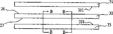
本发明为一种超距感应式光盘片制作方法,为方便说明,以预录型小型光盘片的实施为例,请参阅图3,为本发明超距感应式光盘片制作方法射出成型最佳实施例相对位置示意图。光盘模板31及镜面板33均预先置于射出成型机内,光盘白片32则形成于光盘模板31(stamper)与镜面板33(mirror plate)之间,在射出成型的过程中,塑性材料经光盘模板31与镜面板33双重挤压后,脱模冷却便形成一光盘白片32。该光盘白片有一信息面26与该光盘模板31相接触而形成。该信息面26形成于一数据区13,具有与光盘模板31相对应的坑、洞(pits and lands)或轨道(groove)等信号数据;信息面26的另一面在射出成型时与镜面板33接触而形成一镜面读取面27,该镜面读取面27通常是一光滑的平面。The present invention is a manufacturing method of an ultra-distance induction optical disc. For the convenience of explanation, the implementation of a pre-recorded compact optical disc is taken as an example. Please refer to FIG. The schematic diagram of the relative position of the embodiment. The
请参阅图4,为本发明光盘白片32与镜面板33在中心孔洞11与空白区域12附近的剖面放大示意图(即图3中所示的BB区域),其中镜面板33相对于光盘白片32中心孔洞11外环适当距离处,有一呈环状梯形的第一阶突起部41及第二阶突起部42,该环状第一阶突起部41略低于第二阶突起部42,且位于第二阶突起部42的两侧。由于镜面板33具有环状梯形的突起,使得射出成型后的光盘白片32相应产生环状梯形的第一阶凹陷区411及第二阶凹陷区421。Please refer to FIG. 4 , which is an enlarged cross-sectional schematic view of the disc blank 32 and the
请继续参阅图5,为射出成型后的光盘白片32在镜面读取面的正面视图,正面显示为读取面27,由图中可看出其第一阶凹陷区411及第二阶凹陷区421分布在光盘片上的相对位置,由中心孔洞11往圆周方向,依次为空白区12,第一阶凹陷区411,第二阶凹陷区421,第一阶凹陷区411和空白区域12,空白区的外侧,则为数据区13。Please continue to refer to FIG. 5 , which is a front view of the optical disk
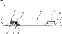
图6所示为本发明的中心孔洞11附近剖面放大示意图,为方便说明起见,右侧与左侧分别绘示本发明实施例中凹陷区后段的制作工艺的实施前及实施后示意图,其中在第二阶凹陷区421中布置绕线组61及一控制芯片62,绕线组61的功能可感应外界的变化磁场,其感应方式以非接触式的超距感应,而控制芯片的作用则捕捉绕线组61特定频率的振荡和电力并通过产生一预定的响应信号,该响应信号可通过芯片的精密控制使其响应信号为唯一且独特,进而将该唯一且独特的信号作为辨识盘片来源或其它控制如开关等的功用,可产生许多不同附加价值的应用。FIG. 6 is an enlarged schematic diagram of a cross-section near the
在第一阶凹陷区411内,为一覆盖层63,以保护并固定位于内部的绕线组61及控制芯片62,覆盖层63的外侧表面631,则与镜面读取面27保持平整。Inside the first-level recessed
尚需说明,上述本发明的超距感应式光盘片制作方法,如图3至图5所示,其中环状梯形突起位于镜面板33的一侧331。同理,也可将环状梯形突起布置于光盘模板31的一侧311,且该环状突起位于空白区域12,并不影响信息面26的信息。另一种可能的环状梯形突起布置方式,设在数据区13的外环区,如实施例的图8外环区81所示,同样可以达到本发明超距感应的目的,唯需注意只要不影响数据的正常读取及能有效感应即可。另外也可在除内环空白区域12或前述外环区81以外的其它信息空白区91设置环状梯形凹陷区,如图9中名片型光盘片的两侧区域等,图中以阴影区域来表现。It needs to be further explained that the above-mentioned method for manufacturing an ultra-distance inductive optical disc of the present invention is shown in FIGS. Similarly, the ring-shaped trapezoidal protrusion can also be arranged on one
另需说明为实施例中的第一阶凹陷区411,其环状梯形布置的目的为增加覆盖层63与光盘白片32的接触面积,以使覆盖层63本身易于固持在第一阶凹陷区内不致因外力而脱落,进而影响盘片本身寿命,倘以不同的加工方式,如热熔接或超音波表面熔结等技术实施,或以射出植入法或适当的UV胶的使用,致覆盖层(即覆盖层73)无脱落之虞时,则可以环状ㄇ形第二阶凹陷区421取代原梯形第一阶凹陷区411;其相对应的镜面板33则可省略梯状的第一阶突起部41,而以第二阶突起部42取代,即如图7中本发明的另一实施例所绘示。It should also be explained that the first-level recessed
依据上述,本发明的超距感应式光盘片制作方法,在射出机内的模具装设具有突起部的镜面板33及一般的光盘模板31,这种装设方式对于射出而言,是较为理想的,但是另外一种相反的安排方式,如以具有突起部的光盘模板和一般的镜面板,也是可以被实施的。突起部可以呈现环状或是环状梯形的布置,以一体射出成型具有相对凹陷区的光盘白片,突起部及凹陷区的位置可以在光盘内环空白区域,或是在光盘外环空白区域,或是其它适当位置。According to the above, in the method for making an ultra-distance inductive optical disc of the present invention, a
具有凹陷区的光盘白片,可以进行光盘的后续制作工艺或是进行凹陷区后段的制作工艺。光盘的后续制作工艺可以包括金属反射层22的溅镀制作工艺、一保护层23的旋涂制作工艺及一印刷制作工艺等,以完成一光盘片本身的完整制作工艺。凹陷区的后段制作工艺则包括在光盘的凹陷区内进行绕线组61制作工艺以形成绕线圈,同时埋设一芯片62,并使该绕线圈61与该芯片62形成一电气回路,再进行一覆盖层63/覆盖层73的制作工艺于该凹陷区,以形成一覆盖层而保护及固定位于内部的该绕线组61及该控制芯片62,并使其外侧表面与光盘片的外表面保持平整。上述的两制作工艺原则上彼此并不互相干扰,若在射出有凹陷区的光盘白片后,先进行光盘的后续制作工艺,好处是其制作工艺几乎完全不受光盘白片是否有凹陷区的影响,甚至可以在凹陷区内表面411F及421F涂布光泽的色彩,以进一步美化光盘片完成后的外观。另外,在光盘的后续制作工艺中,也可因地因时的需要,插入进行凹陷区后段的制作工艺,例如待机、待料或消除瓶颈制作工艺的考虑等。The disc white sheet with the depressed area can be used for the subsequent production process of the optical disc or the subsequent production process for the depressed area. The subsequent manufacturing process of the optical disc may include the sputtering manufacturing process of the metal reflective layer 22, the spin-coating manufacturing process of a protective layer 23, and the printing manufacturing process, etc., so as to complete the complete manufacturing process of the optical disc itself. The post-production process of the recessed area includes performing the manufacturing process of the winding
对于小量或其它特殊、个别考虑下的制造,本发明的超距感应式光盘片制作方法,也可以铣床在一般的光盘片上,铣出环状梯形的第一阶凹陷区411及第二阶凹陷区421,其方法包括于光盘片的一面,进行一环状或环状梯形旋铣的制作工艺,以形成一环状或环状梯形凹陷区,其中该光盘片进行旋铣之位置,位于光盘内环空白区域,或是在光盘外环区域,或是其它适当空间位置。并于该环状凹陷区内进行凹陷区的后段制作工艺,包括在光盘的凹陷区内进行绕线组制作工艺以形成绕线圈,同时埋设一芯片,并使该绕线圈与该芯片形成一电气回路,及进行一覆盖层的制作工艺以达保护和固定位于内部的该绕线组及该控制芯片,并使其外侧表面与光盘片的外表面保持平整。For small quantities or other special and individual considerations, the manufacturing method of the ultra-distance inductive optical disc of the present invention can also mill out the annular trapezoidal first-order recessed
除此之外,热熔印的方式,也是可以被接受的方法,即以热熔印压印的方式,例如使用一热压模,在光盘片的适当区域,如内环空白区内,制作一环状或环状梯形突起部,以在光盘片的适当位置产生相对凹陷区,同样可以达到进行凹陷区后段制作工艺的目的,不过这样的施作方法,对于少量生产,有其正面的意义,但对于大量的生产,反而增加了不必要的加工程序,如所产生的毛边,须进行剪修毛边等工作等,反使成本增加。In addition, the method of hot-melt printing is also acceptable, that is, by hot-melt embossing, for example, using a hot stamping mold, on a suitable area of the optical disc, such as the inner ring blank area, to make A ring-shaped or ring-shaped trapezoidal protrusion can produce a relatively depressed area at an appropriate position on the optical disc, which can also achieve the purpose of carrying out the post-production process of the depressed area. Meaning, but for a large number of production, unnecessary processing procedures are added instead, such as the burrs generated, the burrs must be trimmed, etc., which increases the cost.
本发明所举的各实施例,并非用以限定本发明,任何运用本发明的精神所为之各种变化,如因不同规格光盘片本身不同的特殊制作工艺、或将其制作工艺内容顺序作些许之相关的调整等效变化等,均仍为本发明的申请专利范围所当然涵盖。The various embodiments cited in the present invention are not intended to limit the present invention, and any various changes made by using the spirit of the present invention, such as the special production process due to the different specifications of the optical disc itself, or the sequence of the production process content Some related adjustments, equivalent changes, etc., are still covered by the scope of the patent application of the present invention.
Claims (15)
Priority Applications (1)
| Application Number | Priority Date | Filing Date | Title |
|---|---|---|---|
| CNB021275920A CN1257503C (en) | 2002-08-01 | 2002-08-01 | Method for making ultra-distance inductive optical disk |
Applications Claiming Priority (1)
| Application Number | Priority Date | Filing Date | Title |
|---|---|---|---|
| CNB021275920A CN1257503C (en) | 2002-08-01 | 2002-08-01 | Method for making ultra-distance inductive optical disk |
Publications (2)
| Publication Number | Publication Date |
|---|---|
| CN1472734A CN1472734A (en) | 2004-02-04 |
| CN1257503C true CN1257503C (en) | 2006-05-24 |
Family
ID=34143563
Family Applications (1)
| Application Number | Title | Priority Date | Filing Date |
|---|---|---|---|
| CNB021275920A Expired - Fee Related CN1257503C (en) | 2002-08-01 | 2002-08-01 | Method for making ultra-distance inductive optical disk |
Country Status (1)
| Country | Link |
|---|---|
| CN (1) | CN1257503C (en) |
-
2002
- 2002-08-01 CN CNB021275920A patent/CN1257503C/en not_active Expired - Fee Related
Also Published As
| Publication number | Publication date |
|---|---|
| CN1472734A (en) | 2004-02-04 |
Similar Documents
| Publication | Publication Date | Title |
|---|---|---|
| CA2135279C (en) | Disk-shaped optical storage medium and method for its fabrication | |
| EP1343153B1 (en) | Optical recording medium, optical recording medium production method, optical recording medium production apparatus, program, and medium | |
| US6246656B1 (en) | Reduced thickness of a light transmissive layer for a high density optical disc | |
| EP1291874B1 (en) | Method and apparatus for reducing the shrinkage of an optical disc's clamp area, and the resulting optical disc | |
| US7457227B2 (en) | Optical disc | |
| US5604726A (en) | Pre-format configuration of optical disks and method of data processing using the same | |
| US7710854B2 (en) | Multi-layer optical disc format | |
| CN1257503C (en) | Method for making ultra-distance inductive optical disk | |
| CN1666281A (en) | Information carrier provided with a transitional region between the clambing area and the information area | |
| WO1994010684A1 (en) | Optically readable information disc including visible ornamental hologram, and method of fabricating same | |
| JP2004103170A (en) | Optical pickup | |
| WO1997041557A1 (en) | Process for producing an optical information carrier and optical information carrier | |
| JP2003006936A (en) | High-density optical disk having center hole of asymmetrical upper and lower structure and manufacturing method therefor | |
| JP2003242680A (en) | Disk-shaped optical recording medium | |
| US20050046689A1 (en) | Optical disk medium, optical disk medium production method, turntable and optical disk apparatus | |
| KR100286295B1 (en) | High Density / Low Density Optical Discs | |
| JP3483539B2 (en) | Stamper, mold system, recording medium substrate, stamper manufacturing method | |
| US20030218968A1 (en) | Vacuum-resistant compact disc | |
| KR100565071B1 (en) | Manufacturing method of stamper for substrate manufacturing for optical disk | |
| JP2005032392A (en) | Optical information recording medium and manufacturing method thereof | |
| CN2426191Y (en) | Composite Smart Optical Card | |
| JPH09293279A (en) | Stamper for injection molding of substrate of optical recording medium and manufacturing method thereof | |
| US7785689B2 (en) | Raw material conserving optical data storage media | |
| KR20050032302A (en) | Substrate for optical disc, optical disc employing the substrate and method for manufacturing the same, and stamper for manufacturing the substrate and method for making the stamper | |
| TWI380292B (en) | Image optical storage medium and method for manufacturing the same |
Legal Events
| Date | Code | Title | Description |
|---|---|---|---|
| C06 | Publication | ||
| PB01 | Publication | ||
| C10 | Entry into substantive examination | ||
| SE01 | Entry into force of request for substantive examination | ||
| C14 | Grant of patent or utility model | ||
| GR01 | Patent grant | ||
| C19 | Lapse of patent right due to non-payment of the annual fee | ||
| CF01 | Termination of patent right due to non-payment of annual fee |