CN1229536A - Single ended forward DC-to-DC converter providing enhanced resetting for synchronous rectification - Google Patents
Single ended forward DC-to-DC converter providing enhanced resetting for synchronous rectification Download PDFInfo
- Publication number
- CN1229536A CN1229536A CN97196460A CN97196460A CN1229536A CN 1229536 A CN1229536 A CN 1229536A CN 97196460 A CN97196460 A CN 97196460A CN 97196460 A CN97196460 A CN 97196460A CN 1229536 A CN1229536 A CN 1229536A
- Authority
- CN
- China
- Prior art keywords
- mentioned
- switch
- mosfet
- former
- transducer
- Prior art date
- Legal status (The legal status is an assumption and is not a legal conclusion. Google has not performed a legal analysis and makes no representation as to the accuracy of the status listed.)
- Granted
Links
Images


Classifications
-
- H—ELECTRICITY
- H02—GENERATION; CONVERSION OR DISTRIBUTION OF ELECTRIC POWER
- H02M—APPARATUS FOR CONVERSION BETWEEN AC AND AC, BETWEEN AC AND DC, OR BETWEEN DC AND DC, AND FOR USE WITH MAINS OR SIMILAR POWER SUPPLY SYSTEMS; CONVERSION OF DC OR AC INPUT POWER INTO SURGE OUTPUT POWER; CONTROL OR REGULATION THEREOF
- H02M3/00—Conversion of dc power input into dc power output
- H02M3/22—Conversion of dc power input into dc power output with intermediate conversion into ac
- H02M3/24—Conversion of dc power input into dc power output with intermediate conversion into ac by static converters
- H02M3/28—Conversion of dc power input into dc power output with intermediate conversion into ac by static converters using discharge tubes with control electrode or semiconductor devices with control electrode to produce the intermediate ac
- H02M3/325—Conversion of dc power input into dc power output with intermediate conversion into ac by static converters using discharge tubes with control electrode or semiconductor devices with control electrode to produce the intermediate ac using devices of a triode or a transistor type requiring continuous application of a control signal
- H02M3/335—Conversion of dc power input into dc power output with intermediate conversion into ac by static converters using discharge tubes with control electrode or semiconductor devices with control electrode to produce the intermediate ac using devices of a triode or a transistor type requiring continuous application of a control signal using semiconductor devices only
- H02M3/33569—Conversion of dc power input into dc power output with intermediate conversion into ac by static converters using discharge tubes with control electrode or semiconductor devices with control electrode to produce the intermediate ac using devices of a triode or a transistor type requiring continuous application of a control signal using semiconductor devices only having several active switching elements
- H02M3/33576—Conversion of dc power input into dc power output with intermediate conversion into ac by static converters using discharge tubes with control electrode or semiconductor devices with control electrode to produce the intermediate ac using devices of a triode or a transistor type requiring continuous application of a control signal using semiconductor devices only having several active switching elements having at least one active switching element at the secondary side of an isolation transformer
-
- H—ELECTRICITY
- H02—GENERATION; CONVERSION OR DISTRIBUTION OF ELECTRIC POWER
- H02M—APPARATUS FOR CONVERSION BETWEEN AC AND AC, BETWEEN AC AND DC, OR BETWEEN DC AND DC, AND FOR USE WITH MAINS OR SIMILAR POWER SUPPLY SYSTEMS; CONVERSION OF DC OR AC INPUT POWER INTO SURGE OUTPUT POWER; CONTROL OR REGULATION THEREOF
- H02M3/00—Conversion of dc power input into dc power output
- H02M3/22—Conversion of dc power input into dc power output with intermediate conversion into ac
- H02M3/24—Conversion of dc power input into dc power output with intermediate conversion into ac by static converters
- H02M3/28—Conversion of dc power input into dc power output with intermediate conversion into ac by static converters using discharge tubes with control electrode or semiconductor devices with control electrode to produce the intermediate ac
- H02M3/325—Conversion of dc power input into dc power output with intermediate conversion into ac by static converters using discharge tubes with control electrode or semiconductor devices with control electrode to produce the intermediate ac using devices of a triode or a transistor type requiring continuous application of a control signal
- H02M3/335—Conversion of dc power input into dc power output with intermediate conversion into ac by static converters using discharge tubes with control electrode or semiconductor devices with control electrode to produce the intermediate ac using devices of a triode or a transistor type requiring continuous application of a control signal using semiconductor devices only
- H02M3/33569—Conversion of dc power input into dc power output with intermediate conversion into ac by static converters using discharge tubes with control electrode or semiconductor devices with control electrode to produce the intermediate ac using devices of a triode or a transistor type requiring continuous application of a control signal using semiconductor devices only having several active switching elements
- H02M3/33576—Conversion of dc power input into dc power output with intermediate conversion into ac by static converters using discharge tubes with control electrode or semiconductor devices with control electrode to produce the intermediate ac using devices of a triode or a transistor type requiring continuous application of a control signal using semiconductor devices only having several active switching elements having at least one active switching element at the secondary side of an isolation transformer
- H02M3/33592—Conversion of dc power input into dc power output with intermediate conversion into ac by static converters using discharge tubes with control electrode or semiconductor devices with control electrode to produce the intermediate ac using devices of a triode or a transistor type requiring continuous application of a control signal using semiconductor devices only having several active switching elements having at least one active switching element at the secondary side of an isolation transformer having a synchronous rectifier circuit or a synchronous freewheeling circuit at the secondary side of an isolation transformer
-
- Y—GENERAL TAGGING OF NEW TECHNOLOGICAL DEVELOPMENTS; GENERAL TAGGING OF CROSS-SECTIONAL TECHNOLOGIES SPANNING OVER SEVERAL SECTIONS OF THE IPC; TECHNICAL SUBJECTS COVERED BY FORMER USPC CROSS-REFERENCE ART COLLECTIONS [XRACs] AND DIGESTS
- Y02—TECHNOLOGIES OR APPLICATIONS FOR MITIGATION OR ADAPTATION AGAINST CLIMATE CHANGE
- Y02B—CLIMATE CHANGE MITIGATION TECHNOLOGIES RELATED TO BUILDINGS, e.g. HOUSING, HOUSE APPLIANCES OR RELATED END-USER APPLICATIONS
- Y02B70/00—Technologies for an efficient end-user side electric power management and consumption
- Y02B70/10—Technologies improving the efficiency by using switched-mode power supplies [SMPS], i.e. efficient power electronics conversion e.g. power factor correction or reduction of losses in power supplies or efficient standby modes
Abstract
A single ended forward DC-to-DC converter includes a transformer having a. primary winding electrically connected to a primary switch and a secondary winding electrically connected to a secondary switch and a clamping capacitor. The clamping capacitor stores the magnetization energy from the secondary winding when the primary switch is turned off, thus causing the transformer core to be reset during the period that the primary switch remains off. The converter can use mosfets as the primary and secondary switches, such that a change in the voltage at the secondary winding of the transformer, due to the turning off of the primary switch, results in an automatic turning on of the secondary switch. The combination of the clamping capacitor and the mosfet switches increases the simplicity of the DC-to-DC converter while eliminating undesirable characteristics such as dead time and voltage stresses on the switches. The DC-to-DC converter of the present invention can be used to carry out synchronous rectification and zero voltage switching.
Description
To the DC transducer
The present invention relates to a kind of DC to DC transducer, particularly relate to and have a kind of single ended forward DC-to-DC converter providing that makes the circuit that transformer core resets.
DC to DC transducer is used to convert the dc voltage of input the dc voltage of different outputs to offer load.This transducer generally includes one and is connected electrically in transformer between voltage source and the load by switching circuit.The transducer that is called as single-ended forward converter is a kind of like this transducer, and it relies on the single switch that is connected between voltage source and the transformer primary winding that the power of forward conveying is provided to the auxiliary winding of transformer when switch connection and conduction.
In order to allow the leakage inductance of transformer discharge, transformer core " is resetted " at the switch off period.Normally adopting additional circuit to finish and reset, for example is one the 3rd Transformer Winding with the parallel connection of transformer primary winding, or is electrically connected to a Lc resonant circuit on the auxiliary winding.Yet, having one " idle time " (" dead time ") in the drive waveforms of sort circuit, switch is still kept disconnection during this period, and the voltage of switch ends equals the voltage of voltage source, and does not have electric current.Can reduce the whole efficiency of transducer idle time, and produce voltage stress on switch.
The purpose of this invention is to provide a kind of single ended forward DC-to-DC converter providing (single-ended forward I) C-to-DC converter that can make the transformer core active homing), and do not have idle time basically, make the voltage stress minimum that acts on the commutator assemble.
The present invention relates to a kind of single ended forward DC-to-DC converter providing that can make transformer core active homing (reset), thereby improve the ability that it carries out self-device synchronous rectification.In one embodiment, transducer comprises a transformer, and its primary winding is electrically connected to a former switch, and auxiliary winding is electrically connected to an auxiliary switch and a clamping capacitance device.Auxiliary winding is electrically connected to a pair of rectifier and a LC filter circuit, is used for carrying out rectification and level and smooth for the power signal that arrives load.When former switch is switched on, the primary winding conduction, and at input voltage of auxiliary winding two ends generation.When former switch was disconnected, auxiliary winding was switched on, and the magnetizing current that will be present in the auxiliary winding is transported to the clamping capacitance device, and the clamping capacitance device is charged to was substantially equal to input voltage.During former switch was disconnected, the voltage at auxiliary winding two ends was remained unchanged, and transformer core is resetted.
In other embodiments of the invention, former and auxiliary switch comprises switch mosfet.In such an embodiment, when former switch mosfet was disconnected, the voltage that appears on the auxiliary winding made the MOSFET auxiliary switch enter conducting state.In other embodiments, former switch comprises a kind of n-channel mosfet, and auxiliary switch comprises a kind of p-channel mosfet.In a further embodiment, auxiliary switch comprises a kind of n-channel mosfet, and auxiliary winding is electrically connected to the tertiary winding.Provide starting n one channel mosfet needed positive voltage by the tertiary winding.
Other embodiment of the present invention relate to a kind of method, by starting and closing a former MOSFET who is connected to the transformer primary winding iron core of transformer is resetted, when former MOSFET is closed, secondary MOSFET is started, a clamping capacitance device is charged, and auxiliary winding is clamped at the voltage of clamping capacitance device.
Synchronous rectification provided by the invention and zero voltage switching technology can be used to load that lower output voltage and higher power density are provided effectively.In addition, use clamping capacitance device and switch mosfet that DC to DC transducer is further simplified, and eliminate undesirable idle time and the voltage stress that occurs on the switch.
Can recognize above-mentioned and other features of the present invention according to the following description and claims.
Feature of the present invention has been proposed in appending claims.By following with reference to the description of the drawings above-mentioned and other advantage that the present invention may be better understood, in the accompanying drawings:
Fig. 1 is a kind of single ended forward DC-to-DC converter providing according to one embodiment of the invention;
Fig. 2 A is the single ended forward DC-to-DC converter providing according to another embodiment of the present invention;
Fig. 2 B is the conducting schematic diagram of single ended forward DC-to-DC converter providing when former switch connection of Fig. 2 A;
Fig. 2 C is the conducting schematic diagram of single-ended forward Dc to DC transducer when former switch disconnects of Fig. 2 A;
Fig. 3 A is the single ended forward DC-to-DC converter providing according to further embodiment of this invention;
Fig. 3 B is the conducting schematic diagram of single ended forward DC-to-DC converter providing when former switch connection of Fig. 3 A;
Fig. 3 C is the conducting schematic diagram of single ended forward DC-to-DC converter providing when former switch disconnects of Fig. 3 A;
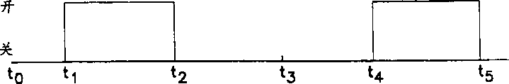
Fig. 4 A is an oscillogram, and the former switch of expression single ended forward DC-to-DC converter providing is switched on the waveform with off period;
Fig. 4 B is an oscillogram, represents that former switch is switched on off period to appear at voltage on the transformer primary winding of single ended forward DC-to-DC converter providing;
Fig. 4 c is an oscillogram, represents that former switch is switched on off period to appear at voltage on the former switch of single ended forward DC-to-DC converter providing:
Fig. 4 D is an oscillogram, represents that former switch is switched on off period to appear at voltage on the transformer auxiliary winding of single ended forward DC-to-DC converter providing.
An embodiment who in Fig. 1, has represented single ended forward DC-to-DC converter providing.As shown in FIG., transformer 10 by electric coupling between DC power supply 20 with certain input voltage V and load 50.Transformer 1O comprises a primary winding 12 and an auxiliary winding 14.The number of turn of winding normally depends on load 50 needed output voltages.For example the typical input voltage in telecommunications industry is 48V, and the typical output voltage that needs is 4V, and therefore, required turn ratio approximately is 12: 1.
Yet for convenience of explanation, the turn ratio of supposing transformer 10 is 1: 1.The former switch of representing with Q1 16 is electrically connected in series between primary winding 12 and the power supply 20.When switch 16 is switched on, just when switch 16 is in closure state, just formed closed circuit, electric current returns power supply 20 after power supply 20 is flowed through primary winding 12, induce a voltage in auxiliary winding 14.
Auxiliary switch 22 and the clamping capacitance device 24 represented with Q2 are electrically connected in series with auxiliary winding 14.Described in hereinafter, clamping capacitance device 24 charges when auxiliary switch 22 is switched on.A diode 26 of representing with Dl is electrically connected in series with the auxiliary winding 14 of transformer 10, and with auxiliary switch 22 and clamping capacitance device 24 in parallel electrical connections.As mentioned below, conducting when diode 26 is switched at former switch 16.One second diode of representing with D2 28 is electrically connected with auxiliary winding 14 parallel connections of transformer 1 O.A Lc circuit 30 is electrically connected to auxiliary winding 14 and diode 26.Lc circuit 30 comprises the filter inductor 32 of connecting with auxiliary winding 14 and diode 28, and a filtering capacitor 34 in parallel with auxiliary winding 14 and diode 28.Diode 26,28 and Lc circuit 30 have constituted a rectification and smoothing circuit jointly, and the voltage to auxiliary winding before offering load 50 carries out filtering.
A control device 40 is electrically connected to former switch 16 and auxiliary switch 22.Control the operation of former switch 16 and auxiliary switch 22 with control device 40, they are switched on and off in desired time.Control device 40 is preferably according to different phase place starting switchs 16,22, and in the present embodiment, control device 40 can produce the delay of a little time when switch 16 and 22 all is in off-state.Auxiliary switch 22 after being disconnected, is connected through behind the predetermined amount of time by former switch 16.Just can realize zero voltage switching by this delay, because the voltage on the former switch 16 can turn back to approximately zero volt before former switch 16 is connected once more.As mentioned below, at this timing period, the magnetizing current that appears at after former switch 16 is disconnected among the transformer 1O is used to keep a constant voltage on auxiliary winding.
When control device 40 was connected former switch 16, the electric current primary winding 12 of flowing through induced electric current in auxiliary winding 14, and this electric current flows to lc circuit 30 through diode 26.With the voltage on the lc circuit 30 level and smooth auxiliary winding 14, in load 50, obtain a DC output.When control device 40 disconnected former switch 16, the electric current of carrying by primary winding 12 and auxiliary winding 14 forwards had just disappeared.At this moment, diode 28 becomes conducting, and the magnetic field energy that is stored in the filter inductor 32 is discharged to filtering capacitor 34 and load 50.Simultaneously the magnetizing current in the transformer is stored in the clamping capacitance device 24, thereby the voltage on the auxiliary winding 14 of transformer 10 is clamped at basically the amplitude of input voltage.It is constant that voltage on the auxiliary winding 14 is kept basically, and because the flux-reversal in the transformer impels transformer 10 to reset.
The electric capacity of clamping capacitance device 34 is enough big, and the voltage at two ends and time relation can be ignored on the clamping capacitance device 34.Under the condition of stable state, be applied to voltage product second on the primary winding 12 of transformer 10 at the time durations that former switch 16 is switched on and equal to be applied to voltage product second (volt-second product) on the auxiliary winding 14 at the time durations that former switch 16 is disconnected.For turn ratio is that 1: 1 transformer 1O can be expressed as:
(V
In) (t
On)=(V
c) (t
Off) or be expressed as:
V
c=(V
Ln) (D/I-D), D wherein is a duty cycle, t
OnBe former switch 16 connect the time interval, and t
OrtBe former switch 16 disconnect the time interval.
Fig. 2 A has represented another embodiment of single ended forward DC-to-DC converter providing of the present invention.As shown in FIG., transformer 110 is connected electrically between DC power supply 120 with certain input voltage V and the load 150.Transformer 11O comprises a primary winding 112 and an auxiliary winding 114.The former switch of representing with Q3 116 of a n-channel mosfet is electrically connected in series with primary winding 112.118, one DC power supplys 120 of drain electrode end that primary winding 112 is electrically connected to MOSFET 116 are electrically connected to the source terminal 122 of MOSFET 116.In the present embodiment, control device 140 is electrically connected to the gate terminal 124 of MOSFET 116, and provides a voltage to grid 124, makes selectively conducting of MOSFET 116.When MOSFET 116 conductings, it and primary winding 112 and DC power supply 120 have constituted the circuit of a closure.A kind of distressed structure as foregoing circuit, if the input polarity on MOSFET 116 drain electrode ends 118 makes MOSFET 116 become forward conduction, and make its reverse bias from the input of controlling device 140 according to coming on the gate terminal 124, just DC power supply 120 can be electrically connected to drain electrode end 118, and primary winding 112 is electrically connected to source terminal 122.
A n-channel mosfet rectifier 126 of representing with D3 is electrically connected in series with the auxiliary winding 114 of transformer 1O.As mentioned below, conducting when rectifier 126 is connected at MOSFET 116.Rectifier 126 is in parallel with auxiliary switch 130 and clamping capacitance device 132.In the present embodiment, auxiliary switch 130 is p-channel mosfets of representing with Q4.The drain electrode end 136 of p-channel mosfet 130 and gate terminal 138 are connected auxiliary winding 114 two ends, allow MOSFET 130 enter forward bias according to the change in voltage at auxiliary winding 114 two ends.Its source terminal 139 is connected to a clamping capacitance device 132.A n-channel mosfet second rectifier of representing with D4 134 is electrically connected in series with clamping capacitance device 132, and in parallel with the auxiliary winding 114 of transformer 110.A lc circuit 160 is electrically connected to auxiliary winding 114 and rectifier 134.With mentioned above similar, lc circuit 160 comprises a filter inductor 162 of connecting with auxiliary winding 114 and rectifier 134, and a filtering capacitor 164 in parallel with auxiliary winding 114 and rectifier 134.Rectifier 126 and 134 function provide self-device synchronous rectification.Rectifier 126 and l 34 have reduced input voltage, and the voltage that appears on the lc circuit is reduced.Rectifier 126 and 134 and lc circuit 160 constituted a rectification and smoothing circuit.
With reference to figure 2B, Fig. 2 B is the conduction schematic diagram of converter circuit part when control device 140 is connected the n-channel mosfet Q3 of former switch 116 of Fig. 2 A.When MOSFET 116 conductings, just formed the circuit of a closure, the input voltage that appears at primary winding 112 two ends makes electric current flow through the primary winding 112 of transformer 110 from voltage source 120, and induces a voltage in auxiliary winding 114.Voltage on the auxiliary winding 114 makes rectifier 126 forward bias, and makes electric current flow through lc circuit 160.Smoothly appear at the voltage at auxiliary winding 114 two ends with lc circuit 160, and in load 150, obtain a DC output.
With reference to figure 2C, Fig. 2 C is the conduction schematic diagram of converter circuit part when control device 140 disconnects n-channel mosfet 116 of Fig. 2 A.Between DC power supply 120 and primary winding 112 and MOSFET 116 connection that dots is arranged, expression does not have electric current to flow through primary winding 112 and MOSFET116.When n channel mosfet 116 was reverse biased, the electric current of carrying to auxiliary winding 114 forwards by primary winding 112 had just stopped.Voltage on the auxiliary winding 114 makes the rectifier 134 of n-channel mosfet D4 become forward bias, and the electric current that the energy that is stored in the filter inductor 162 is discharged enters filtering capacitor 164 and load 15O.Simultaneously, the voltage on the auxiliary winding 4 makes auxiliary switch 130 conductings that p-channel mosfet Q4 constitutes.Like this, the magnetizing current in the auxiliary winding 114 just can 136 flow to source electrode 139 from draining, to 132 chargings of clamping capacitance device.At n-channel mosfet 116 off periods, clamping capacitance device 132 is clamped at input voltage V basically with the voltage on the auxiliary winding 114 of transformer 11O.Self-driven characteristic that it should be noted that the auxiliary switch 130 that obtains with MOSFET Q4 does not especially need control device 140 is connected to and is used for controlling its conducting and disconnection on the MOSFET 130.
Please refer to Fig. 3 A, Fig. 3 A has represented another embodiment of single ended forward DC-to-DC converter providing of the present invention.As shown in FIG., transformer 210 is connected electrically between DC power supply 220 with certain input voltage and the load 250.Transformer 2lO comprises a primary winding 212 and an auxiliary winding 214.The former switch of representing with Q5 216 of a n-channel mosfet is electrically connected in series with primary winding 212.Primary winding 212 is connected electrically between the drain electrode end 218 and Dc power supply 220 of MOSFET 216, and power supply 220 is electrically connected to the source terminal 222 of MOSFET 216.As mentioned above, if the working method of MOSFET 216 remains unchanged, the connection of MOSFET 216 terminals can be different from primary winding 212 and voltage source 220.A control device 240 is electrically connected to the gate terminal 224 of MOSFET 216, and provides a voltage, make MOSFET 216 conductings selectively to grid 224.When MOSFET 216 conductings, it and primary winding 112 and voltage source 120 constitute the circuit of a closure.
The n one channel mosfet auxiliary switch of representing with Q6 230 is electrically connected in series with auxiliary winding 214, when the former switch of n-channel mosfet Q5 is disconnected, and auxiliary switch 230 conductings.The gate terminal 238 of n channel mosfet 230 is electrically connected to the transformer tertiary winding 237 that the output with drain electrode end 236 is in parallel.The tertiary winding 237 provides positive voltage required when making its conducting for auxiliary switch 230.The source terminal 239 of MOSFET 230 is electrically connected to a clamping capacitance device 232.A n-channel mosfet rectifier 226 of representing with D5 also is electrically connected in series with the auxiliary winding 214 of transformer 210.When MOSFET 216 conductings, rectifier 226 is with regard to conducting.Rectifier 226 is also in parallel with auxiliary switch 230 and clamping capacitance device 2 32 that MOSFET Q6 constitutes.A n one channel mosfet second rectifier of representing with D6 2 34 is electrically connected in series with clamping capacitance device 232, and in parallel with the auxiliary winding 214 of transformer 21O.There is a lc circuit 260 to be electrically connected to auxiliary winding 214 and rectifier 234.Lc circuit 260 comprises the filtering capacitor 264 that a filter inductor 262 of connecting with auxiliary winding 214 and rectifier 234 and and auxiliary winding 214 and rectifier 234 are in parallel.As indicated above, rectifier 226 and 234 and lc circuit 260 constituted a rectification and smoothing circuit.
Fig. 3 B has represented the partial circuit diagram of the transducer of Fig. 3 A, its conducting when control circuit 240 makes former switch 216 conductings of n-channel mosfet Q5 formation.When MOSFET Q5 conducting, just form closed circuit, and on drain electrode 218 and source electrode 222 two ends, produced an input voltage, make electric current flow to the primary winding 212 of transformer 210 from voltage source 220, in auxiliary winding 214, induce a voltage.Rectifier 226 forward bias that voltage on the auxiliary winding 214 constitutes MOSFET D5 make electric current flow through lc circuit 260.With the voltage on the lc circuit 260 level and smooth auxiliary winding 214, and in load 250, obtain a DC output.
A partial circuit diagram of the transducer of Fig. 3 C presentation graphs 3A, its conducting when control circuit 240 makes MOSFET 216 conductings.When MOSFET 216 was disconnected, the electric current of carrying by primary winding 212 and auxiliary winding 214 forwards had just stopped.Illustrate once more between DC power supply 220 and primary winding 212 are with OSFET 216 connection that dots is also arranged, expression does not have electric current to flow through MOSFET 216 or primary winding 212. is when MOSFET 216 disconnects, on the tertiary winding 214, positive voltage will occur, make n-channel mosfet 230 become conducting.Self-driven characteristic that it should be noted that the auxiliary switch 230 that obtains with MOSFET Q6 does not especially need control device 240 is connected to and is used for controlling its conducting and disconnection on the switch 230.
Similar to above-mentioned situation, when auxiliary switch 230 conductings, the magnetizing current in the auxiliary winding 214 will 236 flow to source electrode 239 from draining, to 232 chargings of clamping capacitance device.The voltage on the auxiliary winding 214 of transformer 210 is clamped at basically the value of input voltage with clamping capacitance device 232.In addition, the rectifier 234 that the voltage on the auxiliary winding 214 constitutes OSFET D6 becomes forward bias, and the energy that is stored in the filter inductor 262 is discharged to filtering capacitor 264 and load 250.
In each above embodiment, the auxiliary winding of clamping capacitance device and transformer has constituted a resonant circuit, because the clamping capacitance device has reclaimed the magnetic energy of transformer, therefore, the voltage on the transformer can not be lower than the voltage of clamping capacitance device.Therefore, transformer can reset effectively, and has reduced the stress that acts on the former switch.
These features of the present invention in Fig. 4 A-4D, have further been shown.Fig. 4 A has represented the timing diagram of former switch (16,116,216).As shown in FIG., waveform is periodic; Between time t1 and t2, switch (16,116,216) is conducting, and between the t4, switch (16,116,216) disconnects at time t2, between time t4 and t5, and switch (16,116,216) conducting once more.Fig. 4 B has represented the voltage on the primary winding (12,11 2,212) that appears at transformer (10,110,210) in the conducting of former switch (16,116,216) and the break period.As shown in FIG., when former switch (16,116,216) conducting, in the time cycle between time cycle t1 and t2 and t4 and t5 just, primary winding is a high voltage on (12,112,212).When former switch (16,116,216) disconnected, in the time cycle between time cycle t2 and t4 just, primary winding was a low-voltage on (12,112,212).
Fig. 4 C has represented to appear at the voltage on the former switch shown in Fig. 2 A and the 3A (16,116,216).As seen, between time t2 and time t4 that switch disconnects, voltage maintains on the input voltage constant from waveform, and gets back to zero immediately during conducting when switch once more on time t4 and lie prostrate.Fig. 4 D is illustrated in the voltage on the auxiliary winding (14,114,214) that appears at transformer (10,110,210) in the conducting of former switch (16,116,216) and the break period.As shown in FIG., at the t1 of former switch (16,116,216) conducting with in the time cycle between t2 and t4 and the t5, auxiliary winding is a high voltage on (14,114,214). at former switch (116,216) t2 of Duan Kaiing and in the time cycle between the t4, auxiliary winding is a negative voltage on (114,214).Owing to stored the magnetic energy that auxiliary winding (14,114,214) discharges in clamping capacitance device (24,132,232), this voltage is constant in the whole cycle that former switch (16,116,216) disconnects.This negative voltage causes the flow direction in the transformer to change, and transformer core is resetted.
As seen, Dc to the Dc transducer in the foregoing description has been eliminated ubiquitous unnecessary idle time in the conventional transducer from above Fig. 4 A one 4D.In addition, the constant voltage that appears on the auxiliary winding at former switch off period can make transformer core reset effectively.So just improved the function that resets by self, be convenient to it and finish self-device synchronous rectification automatically, this function needs the occasion of low output voltage and high power density in load be useful.
The trend of power transfer technical field is requirement low output voltage and high power density.Synchronous rectification and zero voltage switching also belong to the technology contents that is used for satisfying these requirements.The rectifier that DC to DC transducer of the present invention constitutes can be realized synchronous rectification, has reduced the input voltage of Lc filter circuit under the operating state of out-phase.The present invention has further realized self-device synchronous rectification, because this rectifier is to drive with the voltage on the transformer auxiliary winding.In addition, resetting technique of the present invention has improved synchronous rectification, because the performance of self-device synchronous rectification is to be guaranteed by resetting of transformer core.
The present invention can also realize zero voltage switching.Once more before the conducting, the present invention utilizes the magnetizing current in the transformer that the voltage on the former switch is reduced to a value near zero volt at former switch.So just greatly reduce the power consumption of switch.
Those skilled in the art can also realize various modifications to foregoing under the condition that does not break away from the definite the spirit and scope of the present invention of claims.Therefore, scope of the present invention is not limited in above explanation, but determine by the scope of claims.
Claims (20)
1. self-driven single-ended DC transducer is characterized in that comprising:
The transformer that comprises a primary winding and an auxiliary winding;
Be electrically coupled to the former switch of above-mentioned primary winding, start above-mentioned former switch with an input;
Be electrically coupled to the auxiliary switch of above-mentioned auxiliary winding;
Be electrically coupled to a capacitor of above-mentioned auxiliary switch:
Thus, when first voltage appeared on the above-mentioned auxiliary winding, above-mentioned auxiliary switch was disconnected, when second voltage appears on the above-mentioned auxiliary winding, above-mentioned auxiliary switch is switched on, and with above-mentioned capacitor above-mentioned auxiliary winding is clamped at a constant voltage, makes above-mentioned transformer reset.
2. according to the self-driven single-ended Dc transducer of claim 1, it is characterized in that the conducting after the scheduled time that above-mentioned former switch disconnects of above-mentioned auxiliary switch.
3. according to the self-driven single-ended Dc transducer of claim 1, it is characterized in that above-mentioned former switch and above-mentioned auxiliary switch are MOSFET.
4. self-driven single-ended DC transducer is characterized in that comprising:
The transformer that comprises a primary winding and an auxiliary winding:
Former switch with above-mentioned primary winding series coupled:
Be electrically coupled to the auxiliary switch of above-mentioned auxiliary winding:
Be electrically coupled to a clamping capacitance device of above-mentioned auxiliary winding;
Be electrically coupled to a smoothing circuit of above-mentioned clamping capacitance device and auxiliary winding:
Be electrically coupled to a voltage source of above-mentioned primary winding, be used to provide an input voltage, thereby when above-mentioned former switch conduction, allow electric current flow through the above-mentioned primary winding of above-mentioned transformer, when above-mentioned former switch disconnects, above-mentioned auxiliary winding is in predetermined voltage, makes above-mentioned auxiliary switch conducting, and with above-mentioned clamping capacitance device above-mentioned auxiliary winding is clamped at a constant voltage when above-mentioned former switch disconnects.
5. self-driven single-ended Dc transducer is characterized in that comprising:
The transformer that comprises a primary winding and an auxiliary winding:
The former switch of connecting with above-mentioned primary winding:
The auxiliary switch of connecting, and in parallel with first diode with above-mentioned auxiliary winding, above-mentioned first diode is switched on when above-mentioned auxiliary switch conducting:
A capacitor of connecting with above-mentioned first diode wherein is clamped at above-mentioned first diode and above-mentioned auxiliary winding on one voltage with above-mentioned capacitor when above-mentioned auxiliary switch conducting: and
Provide signal with a control circuit to above-mentioned former switch, above-mentioned switch is out of phase worked to each other.
6. according to the single-ended DC transducer of claim 5, it is characterized in that further comprising second diode of connecting with above-mentioned auxiliary winding, above-mentioned second diode is switched on when above-mentioned former switch conduction.
7. according to the single-ended DC transducer of claim 6, it is characterized in that further comprising an inductor of connecting with above-mentioned second diode.
8. according to the single-ended DC transducer of claim 5, it is characterized in that at above-mentioned former switch when conducting state switches to off-state, be sent to above-mentioned capacitor from the magnetizing current of above-mentioned transformer.
9. according to the single-ended DC transducer of claim 5, it is characterized in that after one of above-mentioned switch is disconnected and before another above-mentioned switch is switched on that above-mentioned control circuit makes above-mentioned former switch and above-mentioned auxiliary switch remain on open position in during preset time.
10. single-ended DC transducer is characterized in that comprising:
The transformer that comprises a primary winding and an auxiliary winding;
The former MOSFET that connects with above-mentioned primary winding;
With the secondary MOSFET that above-mentioned auxiliary winding is connected, above-mentioned secondary MOSFET responds the automatic conducting of voltage on the above-mentioned auxiliary winding;
A capacitor of connecting with above-mentioned secondary MOSFET, above-mentioned capacitor is charged on the voltage when above-mentioned former MOSFET is disconnected; And
Be connected to the control circuit of above-mentioned former MOSFET, be used for making above-mentioned former MOSFET between conducting state and off-state, to replace.
11. according to the single-ended DC transducer of claim 1O, it is characterized in that the drain electrode end of above-mentioned former MOSFET is connected to above-mentioned primary winding, its gate terminal is connected to above-mentioned control circuit.
12., it is characterized in that above-mentioned secondary MOSFET automatic conducting when above-mentioned former MOSFET reaches off-state according to the single-ended DC transducer of claim 11.
13., it is characterized in that above-mentioned secondary MOSFET conducting automatically after the scheduled time that above-mentioned former MOSFET is disconnected according to the single-ended DC transducer of claim 12.
14., it is characterized in that driving above-mentioned former MOSFET, and above-mentioned secondary MOSFET is self-driven with above-mentioned control circuit according to the single-ended DC transducer of claim 10.
15., it is characterized in that above-mentioned former MOSFET is a n-channel mosfet, and above-mentioned secondary MOSFET is a p-channel mosfet according to the single-ended DC transducer of claim 1O.
16., it is characterized in that above-mentioned former MOSFET and above-mentioned secondary MOSFET are n-ditch MOSFET according to the single-ended DC transducer of claim 10.
17., it is characterized in that further comprising a tertiary winding of connecting with above-mentioned auxiliary winding according to the single-ended DC transducer of claim 10.
18., it is characterized in that the grid of above-mentioned secondary MOSFET and drain electrode are connected to the above-mentioned tertiary winding according to the single-ended DC transducer of claim 17.
19., it is characterized in that further comprising a lc circuit with above-mentioned auxiliary winding electric coupling according to the single-ended DC transducer of claim 10.
20. a method that in single-ended DC transducer transformer core is resetted is characterized in that may further comprise the steps:
Make a former MOSFET conducting that is electrically coupled on the transformer primary winding with a control circuit, energy is sent to an auxiliary winding from above-mentioned primary winding;
Disconnect above-mentioned former MOSFET with above-mentioned control circuit, make the automatic conducting of secondary MOSFET of being coupled to above-mentioned auxiliary winding; And
Use a clamping capacitance device charging that is electrically connected in series from the magnetizing current of above-mentioned auxiliary winding pair and above-mentioned secondary MOSFET; And
When above-mentioned former MOSFET keeps disconnection, above-mentioned auxiliary winding is clamped at the charging voltage that equals to be stored in the above-mentioned capacitor, above-mentioned transformer is resetted.
Applications Claiming Priority (4)
| Application Number | Priority Date | Filing Date | Title |
|---|---|---|---|
| US2255596P | 1996-07-18 | 1996-07-18 | |
| US60/022,555 | 1996-07-18 | ||
| US08/730,684 | 1996-10-11 | ||
| US08/730,684 US5781420A (en) | 1996-07-18 | 1996-10-11 | Single ended forward DC-to-DC converter providing enhanced resetting for synchronous rectification |
Publications (2)
| Publication Number | Publication Date |
|---|---|
| CN1229536A true CN1229536A (en) | 1999-09-22 |
| CN1076139C CN1076139C (en) | 2001-12-12 |
Family
ID=26696061
Family Applications (1)
| Application Number | Title | Priority Date | Filing Date |
|---|---|---|---|
| CN97196460A Expired - Fee Related CN1076139C (en) | 1996-07-18 | 1997-07-18 | Single ended forward Dc-to-DC converter providing enhanced resetting for synchronous rectification |
Country Status (7)
| Country | Link |
|---|---|
| US (5) | US5781420A (en) |
| EP (1) | EP0913026B1 (en) |
| KR (1) | KR100481065B1 (en) |
| CN (1) | CN1076139C (en) |
| AT (1) | ATE242562T1 (en) |
| DE (1) | DE69722625T2 (en) |
| WO (1) | WO1998004028A1 (en) |
Cited By (3)
| Publication number | Priority date | Publication date | Assignee | Title |
|---|---|---|---|---|
| CN100388602C (en) * | 2004-12-24 | 2008-05-14 | 中兴通讯股份有限公司 | DC-DC power convertor with low output ripple and low stresses of parts |
| CN101847935A (en) * | 2010-05-24 | 2010-09-29 | 深圳市核达中远通电源技术有限公司 | DC-to-DC converter |
| CN105915060A (en) * | 2016-05-03 | 2016-08-31 | 西安科技大学 | Forward conversion circuit with secondary winding magnetic reset function and reset method thereof |
Families Citing this family (54)
| Publication number | Priority date | Publication date | Assignee | Title |
|---|---|---|---|---|
| US5781420A (en) | 1996-07-18 | 1998-07-14 | International Power Devices, Inc. | Single ended forward DC-to-DC converter providing enhanced resetting for synchronous rectification |
| US7269034B2 (en) | 1997-01-24 | 2007-09-11 | Synqor, Inc. | High efficiency power converter |
| CN1262808A (en) * | 1998-02-03 | 2000-08-09 | 皇家菲利浦电子有限公司 | Switching voltage converter with synchronous rectification |
| US5991171A (en) * | 1998-02-05 | 1999-11-23 | Pi Electronics (H.K.) Ltd. | DC-to-DC converters |
| JP3280615B2 (en) * | 1998-02-18 | 2002-05-13 | ティーディーケイ株式会社 | Switching power supply |
| CN1179475C (en) * | 1998-09-16 | 2004-12-08 | 西门子公司 | Circuit and method for automatic rectification in converters |
| WO2000025413A1 (en) * | 1998-10-23 | 2000-05-04 | Ronald Kevin Fricker | Switch mode and computer power supply with a method of its controlling |
| JP3387456B2 (en) * | 1998-10-29 | 2003-03-17 | 株式会社村田製作所 | Switching power supply |
| US6038148A (en) * | 1998-12-11 | 2000-03-14 | Ericsson, Inc. | Self-driven synchronous rectification scheme |
| US6256214B1 (en) | 1999-03-11 | 2001-07-03 | Ericsson Inc. | General self-driven synchronous rectification scheme for synchronous rectifiers having a floating gate |
| JP3336995B2 (en) * | 1999-04-30 | 2002-10-21 | 株式会社村田製作所 | DC-DC converter |
| ES2157784B1 (en) | 1999-05-06 | 2002-02-16 | Cit Alcatel | POWER CONVERTER SWITCHED TO ZERO VOLTAGE. |
| US6304463B1 (en) * | 1999-05-07 | 2001-10-16 | Power-One, Inc. | Single-ended forward converter circuit with quasi-optimal resetting for synchronous rectification |
| US6369408B1 (en) | 1999-10-06 | 2002-04-09 | Agere Systems Guardian Corp. | GaAs MOSFET having low capacitance and on-resistance and method of manufacturing the same |
| WO2001033708A1 (en) | 1999-11-05 | 2001-05-10 | Power-One, Inc. | Forward converter circuit having reduced switching losses |
| US6163467A (en) * | 1999-12-14 | 2000-12-19 | Nagano Japan Radio Co., Ltd. | Switching power supply for generating DC voltage by synchronous rectification |
| ATE261204T1 (en) * | 2000-06-09 | 2004-03-15 | Cit Alcatel | RESONANCE SWITCHING POWER SUPPLY |
| JP2002153054A (en) * | 2000-11-10 | 2002-05-24 | Fujitsu Ltd | Switching power circuit |
| US6343023B1 (en) * | 2000-12-15 | 2002-01-29 | Celestica International Inc. | System and method for recovering energy in power converters |
| US6625043B2 (en) * | 2001-02-21 | 2003-09-23 | Tdk Corporation | Power supply unit and driving method thereof |
| US6324077B1 (en) | 2001-04-19 | 2001-11-27 | Martek Power, Inc. | Switch mode power supply |
| US6807073B1 (en) | 2001-05-02 | 2004-10-19 | Oltronics, Inc. | Switching type power converter circuit and method for use therein |
| US6452818B1 (en) * | 2001-08-27 | 2002-09-17 | Anastasios A. Simopoulos | Self driven active clamp |
| US6937483B2 (en) * | 2002-01-16 | 2005-08-30 | Ballard Power Systems Corporation | Device and method of commutation control for an isolated boost converter |
| KR100508208B1 (en) * | 2002-09-26 | 2005-08-17 | 동양이엔피 주식회사 | Synchronous rectifier for switching power supplies |
| WO2004036726A1 (en) * | 2002-10-21 | 2004-04-29 | Sanken Electric Co., Ltd. | Dc converter |
| US6939347B2 (en) * | 2002-11-19 | 2005-09-06 | Conmed Corporation | Electrosurgical generator and method with voltage and frequency regulated high-voltage current mode power supply |
| US6882548B1 (en) | 2003-02-24 | 2005-04-19 | Tyco Electronics Power Systems, Inc. | Auxiliary active clamp circuit, a method of clamping a voltage of a rectifier switch and a power converter employing the circuit or method |
| US6822882B1 (en) | 2003-08-01 | 2004-11-23 | Tyco Electronics Power Systems, Inc. | Gate driver with a DC offset bias circuit and a power converter employing the same |
| CN1295854C (en) * | 2003-10-17 | 2007-01-17 | 中兴通讯股份有限公司 | Self-drive reset circuit for single-end ortho-excited powder source |
| FR2861916A1 (en) * | 2003-10-31 | 2005-05-06 | St Microelectronics Sa | CONTROLLING A MOS TRANSISTOR AS A RECOVERY ELEMENT |
| EP1687890A1 (en) * | 2003-11-14 | 2006-08-09 | Koninklijke Philips Electronics N.V. | Optocouplerless switched mode power supply |
| US7130201B2 (en) * | 2004-05-14 | 2006-10-31 | Grand Power Sources Inc. | Power supply device for outputting stable programmable power supply |
| JP4430531B2 (en) * | 2004-12-28 | 2010-03-10 | 株式会社日立製作所 | Bi-directional isolated DC-DC converter |
| US7606051B1 (en) * | 2005-11-03 | 2009-10-20 | Wittenbreder Jr Ernest Henry | Fully clamped coupled inductors in power conversion circuits |
| DE102007060231A1 (en) * | 2007-12-14 | 2009-06-18 | Robert Bosch Gmbh | Generator with rectifier arrangement |
| US7924579B2 (en) * | 2008-02-05 | 2011-04-12 | Cisco Technology, Inc. | Fly-forward converter power supply |
| US9397502B2 (en) | 2009-03-02 | 2016-07-19 | Volterra Semiconductor LLC | System and method for proportioned power distribution in power converter arrays |
| US10283974B2 (en) | 2009-03-02 | 2019-05-07 | Volterra Semiconductor LLC | Systems and methods for intelligent, adaptive management of energy storage packs |
| US8686693B2 (en) * | 2009-03-02 | 2014-04-01 | Volterra Semiconductor Corporation | Systems and methods for scalable configurations of intelligent energy storage packs |
| DE102009055331A1 (en) * | 2009-12-28 | 2011-06-30 | Robert Bosch GmbH, 70469 | Device and method for detecting a reverse polarity on a low-voltage side of a DC-DC converter in a two-voltage on-board network |
| GB2480822B (en) * | 2010-06-01 | 2017-05-17 | Global Inkjet Systems Ltd | Driver circuit |
| CN102170732B (en) * | 2011-04-24 | 2014-02-19 | 魏其萃 | Drive circuit topological device for MR16 (Multifaceted Reflector) light-emitting diode |
| CN102497106A (en) * | 2011-12-05 | 2012-06-13 | 北京新雷能科技股份有限公司 | Single-end forward power inverter |
| JP5641368B2 (en) * | 2012-04-12 | 2014-12-17 | 株式会社村田製作所 | Switching power supply |
| US10199950B1 (en) | 2013-07-02 | 2019-02-05 | Vlt, Inc. | Power distribution architecture with series-connected bus converter |
| KR102344534B1 (en) * | 2014-11-11 | 2021-12-29 | 엘지이노텍 주식회사 | Power converter |
| US10262829B2 (en) * | 2015-12-14 | 2019-04-16 | General Electric Company | Protection circuit assembly and method for high voltage systems |
| IT201900006000A1 (en) * | 2019-04-17 | 2020-10-17 | St Microelectronics Srl | A PROCEDURE FOR OPERATING A FLYBACK CONVERTER WITH AN ACTIVE CLAMP, CORRESPONDING CONTROL CIRCUIT AND FLYBACK CONVERTER |
| CN111682778B (en) * | 2020-06-02 | 2023-06-30 | 西安科技大学 | Magnetic reset forward converter |
| CN111682775B (en) * | 2020-06-02 | 2022-12-09 | 西安科技大学 | Forward converter for realizing excitation energy transfer by serially connecting secondary side with LCD |
| CN111682776B (en) * | 2020-06-02 | 2022-12-09 | 西安科技大学 | Secondary-side parallel LCD forward converter capable of inhibiting output energy from flowing backwards |
| CN111682750B (en) * | 2020-06-02 | 2022-12-30 | 西安摩达芯电子科技有限公司 | Forward converter for realizing forward and backward excitation energy transmission by parallel LCD (liquid crystal display) on secondary side |
| US11804782B2 (en) * | 2022-01-28 | 2023-10-31 | Analog Devices, Inc. | Active-clamp current-fed push-pull converter for bidirectional power transfer |
Family Cites Families (32)
| Publication number | Priority date | Publication date | Assignee | Title |
|---|---|---|---|---|
| SU89614A1 (en) | 1949-08-13 | 1949-11-30 | С.А. Дарбинян | Bakery Oven |
| SU892614A1 (en) * | 1980-04-11 | 1981-12-23 | Московский Ордена Ленина Энергетический Институт | One-cycle dc voltage regulator |
| US4444146A (en) | 1982-01-13 | 1984-04-24 | Honeywell Inc. | Ultrasonic subsurface cleaning |
| US4441146A (en) * | 1982-02-04 | 1984-04-03 | Vicor Corporation | Optimal resetting of the transformer's core in single ended forward converters |
| US4688160A (en) * | 1985-12-19 | 1987-08-18 | American Telephone And Telegraph Co., At&T Bell Labs | Single ended forward converter with resonant commutation of magnetizing current |
| US4809148A (en) * | 1987-10-21 | 1989-02-28 | British Columbia Telephone Company | Full-fluxed, single-ended DC converter |
| US4975821A (en) * | 1989-10-10 | 1990-12-04 | Lethellier Patrice R | High frequency switched mode resonant commutation power supply |
| JPH0748944B2 (en) * | 1989-10-14 | 1995-05-24 | 東光株式会社 | DC-DC converter |
| US5126931A (en) * | 1990-09-07 | 1992-06-30 | Itt Corporation | Fixed frequency single ended forward converter switching at zero voltage |
| US5291382A (en) * | 1991-04-10 | 1994-03-01 | Lambda Electronics Inc. | Pulse width modulated DC/DC converter with reduced ripple current coponent stress and zero voltage switching capability |
| EP0515988B1 (en) * | 1991-05-29 | 1997-01-22 | Siemens Aktiengesellschaft | Single-ended forward converter with a transformer and with a protection circuit for an electronic switch |
| US5353212A (en) * | 1992-04-20 | 1994-10-04 | At&T Bell Laboratories | Zero-voltage switching power converter with ripple current cancellation |
| US5521807A (en) * | 1992-12-31 | 1996-05-28 | Interpoint Corporation | DC-To-DC converter with secondary flyback core reset |
| US5434768A (en) * | 1993-02-12 | 1995-07-18 | Rompower | Fixed frequency converter switching at zero voltage |
| US5303138A (en) * | 1993-04-29 | 1994-04-12 | At&T Bell Laboratories | Low loss synchronous rectifier for application to clamped-mode power converters |
| US5625541A (en) * | 1993-04-29 | 1997-04-29 | Lucent Technologies Inc. | Low loss synchronous rectifier for application to clamped-mode power converters |
| US5457620A (en) * | 1993-07-30 | 1995-10-10 | At&T Ipm Corp. | Current estimating circuit for switch mode power supply |
| US5434767A (en) * | 1994-01-10 | 1995-07-18 | University Of Central Florida | Power converter possessing zero-voltage switching and output isolation |
| US5636106A (en) * | 1994-01-10 | 1997-06-03 | University Of Central Florida | Variable frequency controlled zero-voltage switching single-ended current-fed DC-to-AC converter with output isolation |
| US5610508A (en) * | 1994-06-16 | 1997-03-11 | Reltec Corporation | Circuitry to maintain proper current transformer operation |
| JP3328429B2 (en) * | 1994-06-20 | 2002-09-24 | パイオニア株式会社 | Beam power control device for optical disk recording |
| JP2795217B2 (en) * | 1995-06-01 | 1998-09-10 | 日本電気株式会社 | Synchronous rectification type converter |
| JP2806320B2 (en) * | 1995-09-13 | 1998-09-30 | 日本電気株式会社 | Synchronous rectification circuit |
| JP2792536B2 (en) * | 1995-09-26 | 1998-09-03 | 日本電気株式会社 | Resonant DC-DC converter |
| JPH09103073A (en) * | 1995-10-05 | 1997-04-15 | Fujitsu Denso Ltd | Dc-dc converter |
| US5636107A (en) * | 1995-11-15 | 1997-06-03 | International Power Devices, Inc. | DC-DC converters |
| KR0164098B1 (en) * | 1996-04-02 | 1999-04-15 | 이준 | An active forward converter |
| US5781420A (en) * | 1996-07-18 | 1998-07-14 | International Power Devices, Inc. | Single ended forward DC-to-DC converter providing enhanced resetting for synchronous rectification |
| US5991171A (en) * | 1998-02-05 | 1999-11-23 | Pi Electronics (H.K.) Ltd. | DC-to-DC converters |
| US5999419A (en) * | 1998-08-07 | 1999-12-07 | National Semiconductor Corporation | Non-isolated boost converter with current steering |
| JP2000078841A (en) * | 1998-08-28 | 2000-03-14 | Nec Corp | Rectifier circuit of dc/dc converter |
| US6021051A (en) * | 1998-12-29 | 2000-02-01 | General Electric Company | Power converter with crowbar circuit and control for very fast output voltage turn-off |
-
1996
- 1996-10-11 US US08/730,684 patent/US5781420A/en not_active Expired - Fee Related
-
1997
- 1997-07-18 WO PCT/US1997/012667 patent/WO1998004028A1/en active IP Right Grant
- 1997-07-18 KR KR10-1999-7000377A patent/KR100481065B1/en not_active IP Right Cessation
- 1997-07-18 DE DE69722625T patent/DE69722625T2/en not_active Expired - Fee Related
- 1997-07-18 CN CN97196460A patent/CN1076139C/en not_active Expired - Fee Related
- 1997-07-18 EP EP97936977A patent/EP0913026B1/en not_active Expired - Lifetime
- 1997-07-18 AT AT97936977T patent/ATE242562T1/en not_active IP Right Cessation
-
1998
- 1998-06-26 US US09/105,511 patent/US5886881A/en not_active Expired - Lifetime
-
1999
- 1999-03-10 US US09/266,199 patent/US5986899A/en not_active Expired - Lifetime
- 1999-11-15 US US09/439,748 patent/US6141224A/en not_active Expired - Lifetime
-
2000
- 2000-06-06 US US09/587,943 patent/US6278621B1/en not_active Expired - Fee Related
Cited By (4)
| Publication number | Priority date | Publication date | Assignee | Title |
|---|---|---|---|---|
| CN100388602C (en) * | 2004-12-24 | 2008-05-14 | 中兴通讯股份有限公司 | DC-DC power convertor with low output ripple and low stresses of parts |
| CN101847935A (en) * | 2010-05-24 | 2010-09-29 | 深圳市核达中远通电源技术有限公司 | DC-to-DC converter |
| CN105915060A (en) * | 2016-05-03 | 2016-08-31 | 西安科技大学 | Forward conversion circuit with secondary winding magnetic reset function and reset method thereof |
| CN105915060B (en) * | 2016-05-03 | 2018-07-27 | 西安科技大学 | Forward conversion circuit with vice-side winding magnetic reset function and its repositioning method |
Also Published As
| Publication number | Publication date |
|---|---|
| DE69722625T2 (en) | 2004-05-13 |
| US5781420A (en) | 1998-07-14 |
| US6141224A (en) | 2000-10-31 |
| US6278621B1 (en) | 2001-08-21 |
| EP0913026B1 (en) | 2003-06-04 |
| KR100481065B1 (en) | 2005-04-07 |
| WO1998004028A1 (en) | 1998-01-29 |
| EP0913026A1 (en) | 1999-05-06 |
| KR20000067919A (en) | 2000-11-25 |
| US5886881A (en) | 1999-03-23 |
| DE69722625D1 (en) | 2003-07-10 |
| CN1076139C (en) | 2001-12-12 |
| US5986899A (en) | 1999-11-16 |
| ATE242562T1 (en) | 2003-06-15 |
Similar Documents
| Publication | Publication Date | Title |
|---|---|---|
| CN1229536A (en) | Single ended forward DC-to-DC converter providing enhanced resetting for synchronous rectification | |
| US6452814B1 (en) | Zero voltage switching cells for power converters | |
| US6198260B1 (en) | Zero voltage switching active reset power converters | |
| US5590032A (en) | Self-synchronized drive circuit for a synchronous rectifier in a clamped-mode power converter | |
| US6349044B1 (en) | Zero voltage zero current three level dc-dc converter | |
| USRE37889E1 (en) | Low loss synchronous rectifier for application to clamped-mode power converters | |
| EP0851566B1 (en) | Half-bridge zero-voltage-switched PWM flyback DC/DC converter | |
| US5625541A (en) | Low loss synchronous rectifier for application to clamped-mode power converters | |
| JP4574930B2 (en) | Resonant gate driver for synchronous rectifier | |
| US20050073861A1 (en) | Active resonant snubber for dc-dc converter | |
| US7035120B2 (en) | Driving circuit employing synchronous rectifier circuit | |
| CN1797921B (en) | Synchronous rectifier drive circuit for low output voltage active clamp forward converter | |
| CN101826810A (en) | Synchronous rectifier circuit for switching power supply | |
| CN109980903B (en) | Drive circuit and power supply | |
| US4760512A (en) | Circuit for reducing transistor stress and resetting the transformer core of a power converter | |
| US6043993A (en) | Resonance type switching power source | |
| CN1479441B (en) | Electric regenerative circuit and power conversion device | |
| US7944713B2 (en) | Electric power conversion circuit having transfer gain variable by pulse-width modulation | |
| US11527963B2 (en) | Control unit for improving conversion efficiency | |
| US6650558B1 (en) | Asymmetrical drive circuit for full-wave bridge | |
| KR200266522Y1 (en) | Energy regenerative snubber circuit for 2-switch forward converter | |
| JPH05260739A (en) | Forward converter | |
| EP0770281B1 (en) | Power supply apparatus comprising an improved limiter circuit | |
| CN220896531U (en) | Power supply circuit, power supply system and power supply equipment | |
| CN100461598C (en) | Reset circuit of single-end ortho-exciting electric source |
Legal Events
| Date | Code | Title | Description |
|---|---|---|---|
| C06 | Publication | ||
| PB01 | Publication | ||
| C10 | Entry into substantive examination | ||
| SE01 | Entry into force of request for substantive examination | ||
| C14 | Grant of patent or utility model | ||
| GR01 | Patent grant | ||
| C19 | Lapse of patent right due to non-payment of the annual fee | ||
| CF01 | Termination of patent right due to non-payment of annual fee |