CN1211873C - Magnetic resistance element and magnetic device using same - Google Patents
Magnetic resistance element and magnetic device using same Download PDFInfo
- Publication number
- CN1211873C CN1211873C CNB011372362A CN01137236A CN1211873C CN 1211873 C CN1211873 C CN 1211873C CN B011372362 A CNB011372362 A CN B011372362A CN 01137236 A CN01137236 A CN 01137236A CN 1211873 C CN1211873 C CN 1211873C
- Authority
- CN
- China
- Prior art keywords
- mentioned
- substrate
- magnetosphere
- layer
- magnetoresistive element
- Prior art date
- Legal status (The legal status is an assumption and is not a legal conclusion. Google has not performed a legal analysis and makes no representation as to the accuracy of the status listed.)
- Expired - Fee Related
Links
- 230000005291 magnetic effect Effects 0.000 title claims abstract description 118
- NRTOMJZYCJJWKI-UHFFFAOYSA-N Titanium nitride Chemical compound [Ti]#N NRTOMJZYCJJWKI-UHFFFAOYSA-N 0.000 claims abstract description 51
- 239000000758 substrate Substances 0.000 claims abstract description 49
- 230000005415 magnetization Effects 0.000 claims abstract description 21
- 239000013078 crystal Substances 0.000 claims abstract description 19
- CPLXHLVBOLITMK-UHFFFAOYSA-N magnesium oxide Inorganic materials [Mg]=O CPLXHLVBOLITMK-UHFFFAOYSA-N 0.000 claims description 30
- 239000000395 magnesium oxide Substances 0.000 claims description 19
- XEEYBQQBJWHFJM-UHFFFAOYSA-N iron Substances [Fe] XEEYBQQBJWHFJM-UHFFFAOYSA-N 0.000 claims description 16
- AXZKOIWUVFPNLO-UHFFFAOYSA-N magnesium;oxygen(2-) Chemical compound [O-2].[Mg+2] AXZKOIWUVFPNLO-UHFFFAOYSA-N 0.000 claims description 8
- 230000005294 ferromagnetic effect Effects 0.000 claims description 6
- 229910052742 iron Inorganic materials 0.000 claims description 4
- OSGAYBCDTDRGGQ-UHFFFAOYSA-L calcium sulfate Chemical compound [Ca+2].[O-]S([O-])(=O)=O OSGAYBCDTDRGGQ-UHFFFAOYSA-L 0.000 claims 3
- 238000002425 crystallisation Methods 0.000 claims 2
- 230000008025 crystallization Effects 0.000 claims 2
- 238000001514 detection method Methods 0.000 claims 1
- 238000009413 insulation Methods 0.000 claims 1
- 230000008859 change Effects 0.000 abstract description 30
- 230000000694 effects Effects 0.000 abstract description 14
- 239000000126 substance Substances 0.000 abstract description 3
- 229910052596 spinel Inorganic materials 0.000 abstract 1
- 239000011029 spinel Substances 0.000 abstract 1
- 239000010408 film Substances 0.000 description 27
- 239000000463 material Substances 0.000 description 13
- 238000000034 method Methods 0.000 description 9
- 229910052802 copper Inorganic materials 0.000 description 6
- 239000010949 copper Substances 0.000 description 6
- 239000000696 magnetic material Substances 0.000 description 6
- 229910003321 CoFe Inorganic materials 0.000 description 5
- RYGMFSIKBFXOCR-UHFFFAOYSA-N Copper Chemical compound [Cu] RYGMFSIKBFXOCR-UHFFFAOYSA-N 0.000 description 5
- 239000010409 thin film Substances 0.000 description 5
- 239000004020 conductor Substances 0.000 description 4
- 229910052737 gold Inorganic materials 0.000 description 4
- 239000010931 gold Substances 0.000 description 4
- 238000003860 storage Methods 0.000 description 4
- VTLYFUHAOXGGBS-UHFFFAOYSA-N Fe3+ Chemical compound [Fe+3] VTLYFUHAOXGGBS-UHFFFAOYSA-N 0.000 description 3
- GWEVSGVZZGPLCZ-UHFFFAOYSA-N Titan oxide Chemical compound O=[Ti]=O GWEVSGVZZGPLCZ-UHFFFAOYSA-N 0.000 description 3
- 230000004888 barrier function Effects 0.000 description 3
- 230000015572 biosynthetic process Effects 0.000 description 3
- PCHJSUWPFVWCPO-UHFFFAOYSA-N gold Chemical compound [Au] PCHJSUWPFVWCPO-UHFFFAOYSA-N 0.000 description 3
- JEIPFZHSYJVQDO-UHFFFAOYSA-N iron(III) oxide Inorganic materials O=[Fe]O[Fe]=O JEIPFZHSYJVQDO-UHFFFAOYSA-N 0.000 description 3
- TWNQGVIAIRXVLR-UHFFFAOYSA-N oxo(oxoalumanyloxy)alumane Chemical compound O=[Al]O[Al]=O TWNQGVIAIRXVLR-UHFFFAOYSA-N 0.000 description 3
- BASFCYQUMIYNBI-UHFFFAOYSA-N platinum Chemical compound [Pt] BASFCYQUMIYNBI-UHFFFAOYSA-N 0.000 description 3
- VEALVRVVWBQVSL-UHFFFAOYSA-N strontium titanate Chemical compound [Sr+2].[O-][Ti]([O-])=O VEALVRVVWBQVSL-UHFFFAOYSA-N 0.000 description 3
- OGIDPMRJRNCKJF-UHFFFAOYSA-N titanium oxide Inorganic materials [Ti]=O OGIDPMRJRNCKJF-UHFFFAOYSA-N 0.000 description 3
- 230000007704 transition Effects 0.000 description 3
- XKRFYHLGVUSROY-UHFFFAOYSA-N Argon Chemical compound [Ar] XKRFYHLGVUSROY-UHFFFAOYSA-N 0.000 description 2
- IJGRMHOSHXDMSA-UHFFFAOYSA-N Atomic nitrogen Chemical compound N#N IJGRMHOSHXDMSA-UHFFFAOYSA-N 0.000 description 2
- PXHVJJICTQNCMI-UHFFFAOYSA-N Nickel Chemical compound [Ni] PXHVJJICTQNCMI-UHFFFAOYSA-N 0.000 description 2
- XUIMIQQOPSSXEZ-UHFFFAOYSA-N Silicon Chemical compound [Si] XUIMIQQOPSSXEZ-UHFFFAOYSA-N 0.000 description 2
- FAPWRFPIFSIZLT-UHFFFAOYSA-M Sodium chloride Chemical compound [Na+].[Cl-] FAPWRFPIFSIZLT-UHFFFAOYSA-M 0.000 description 2
- 229910052782 aluminium Inorganic materials 0.000 description 2
- 230000005290 antiferromagnetic effect Effects 0.000 description 2
- 238000005229 chemical vapour deposition Methods 0.000 description 2
- PMHQVHHXPFUNSP-UHFFFAOYSA-M copper(1+);methylsulfanylmethane;bromide Chemical compound Br[Cu].CSC PMHQVHHXPFUNSP-UHFFFAOYSA-M 0.000 description 2
- 238000010586 diagram Methods 0.000 description 2
- 230000006872 improvement Effects 0.000 description 2
- 230000010354 integration Effects 0.000 description 2
- 238000004519 manufacturing process Methods 0.000 description 2
- 230000007246 mechanism Effects 0.000 description 2
- 229910052751 metal Inorganic materials 0.000 description 2
- 239000002184 metal Substances 0.000 description 2
- BPUBBGLMJRNUCC-UHFFFAOYSA-N oxygen(2-);tantalum(5+) Chemical compound [O-2].[O-2].[O-2].[O-2].[O-2].[Ta+5].[Ta+5] BPUBBGLMJRNUCC-UHFFFAOYSA-N 0.000 description 2
- 238000000206 photolithography Methods 0.000 description 2
- 230000008569 process Effects 0.000 description 2
- 238000012545 processing Methods 0.000 description 2
- 230000035945 sensitivity Effects 0.000 description 2
- 229910052710 silicon Inorganic materials 0.000 description 2
- 239000010703 silicon Substances 0.000 description 2
- 235000002639 sodium chloride Nutrition 0.000 description 2
- 239000011780 sodium chloride Substances 0.000 description 2
- 238000004544 sputter deposition Methods 0.000 description 2
- IATRAKWUXMZMIY-UHFFFAOYSA-N strontium oxide Chemical compound [O-2].[Sr+2] IATRAKWUXMZMIY-UHFFFAOYSA-N 0.000 description 2
- 229910001936 tantalum oxide Inorganic materials 0.000 description 2
- VYZAMTAEIAYCRO-UHFFFAOYSA-N Chromium Chemical compound [Cr] VYZAMTAEIAYCRO-UHFFFAOYSA-N 0.000 description 1
- CWYNVVGOOAEACU-UHFFFAOYSA-N Fe2+ Chemical compound [Fe+2] CWYNVVGOOAEACU-UHFFFAOYSA-N 0.000 description 1
- 229910017771 LaFeO Inorganic materials 0.000 description 1
- PWHULOQIROXLJO-UHFFFAOYSA-N Manganese Chemical compound [Mn] PWHULOQIROXLJO-UHFFFAOYSA-N 0.000 description 1
- 229910020068 MgAl Inorganic materials 0.000 description 1
- 229910001199 N alloy Inorganic materials 0.000 description 1
- 229910020018 Nb Zr Inorganic materials 0.000 description 1
- 229910004298 SiO 2 Inorganic materials 0.000 description 1
- VYPSYNLAJGMNEJ-UHFFFAOYSA-N Silicium dioxide Chemical compound O=[Si]=O VYPSYNLAJGMNEJ-UHFFFAOYSA-N 0.000 description 1
- 229910002796 Si–Al Inorganic materials 0.000 description 1
- RTAQQCXQSZGOHL-UHFFFAOYSA-N Titanium Chemical compound [Ti] RTAQQCXQSZGOHL-UHFFFAOYSA-N 0.000 description 1
- 229910045601 alloy Inorganic materials 0.000 description 1
- 239000000956 alloy Substances 0.000 description 1
- XAGFODPZIPBFFR-UHFFFAOYSA-N aluminium Chemical compound [Al] XAGFODPZIPBFFR-UHFFFAOYSA-N 0.000 description 1
- PNEYBMLMFCGWSK-UHFFFAOYSA-N aluminium oxide Inorganic materials [O-2].[O-2].[O-2].[Al+3].[Al+3] PNEYBMLMFCGWSK-UHFFFAOYSA-N 0.000 description 1
- 229910000808 amorphous metal alloy Inorganic materials 0.000 description 1
- 229910052786 argon Inorganic materials 0.000 description 1
- 239000000919 ceramic Substances 0.000 description 1
- 229910000420 cerium oxide Inorganic materials 0.000 description 1
- 229910052804 chromium Inorganic materials 0.000 description 1
- 239000011651 chromium Substances 0.000 description 1
- 229910017052 cobalt Inorganic materials 0.000 description 1
- 239000010941 cobalt Substances 0.000 description 1
- GUTLYIVDDKVIGB-UHFFFAOYSA-N cobalt atom Chemical compound [Co] GUTLYIVDDKVIGB-UHFFFAOYSA-N 0.000 description 1
- 239000002131 composite material Substances 0.000 description 1
- 230000007423 decrease Effects 0.000 description 1
- 238000002050 diffraction method Methods 0.000 description 1
- 238000009713 electroplating Methods 0.000 description 1
- 238000005516 engineering process Methods 0.000 description 1
- 238000011156 evaluation Methods 0.000 description 1
- 230000006870 function Effects 0.000 description 1
- 239000011521 glass Substances 0.000 description 1
- 238000010438 heat treatment Methods 0.000 description 1
- CDRCPXYWYPYVPY-UHFFFAOYSA-N iron(2+) oxygen(2-) Chemical compound [O-2].[O-2].[O-2].[O-2].[Fe+2].[Fe+2].[Fe+2].[Fe+2] CDRCPXYWYPYVPY-UHFFFAOYSA-N 0.000 description 1
- 238000003475 lamination Methods 0.000 description 1
- 229910052748 manganese Inorganic materials 0.000 description 1
- 239000011572 manganese Substances 0.000 description 1
- 239000000203 mixture Substances 0.000 description 1
- 229910052759 nickel Inorganic materials 0.000 description 1
- 150000004767 nitrides Chemical class 0.000 description 1
- 229910052757 nitrogen Inorganic materials 0.000 description 1
- 230000001590 oxidative effect Effects 0.000 description 1
- BMMGVYCKOGBVEV-UHFFFAOYSA-N oxo(oxoceriooxy)cerium Chemical compound [Ce]=O.O=[Ce]=O BMMGVYCKOGBVEV-UHFFFAOYSA-N 0.000 description 1
- 230000035699 permeability Effects 0.000 description 1
- 229910052697 platinum Inorganic materials 0.000 description 1
- 238000011160 research Methods 0.000 description 1
- 229910052594 sapphire Inorganic materials 0.000 description 1
- 239000010980 sapphire Substances 0.000 description 1
- 229910052814 silicon oxide Inorganic materials 0.000 description 1
- 229910052709 silver Inorganic materials 0.000 description 1
- 239000010944 silver (metal) Substances 0.000 description 1
- 238000000992 sputter etching Methods 0.000 description 1
- 239000010936 titanium Substances 0.000 description 1
- 229910052719 titanium Inorganic materials 0.000 description 1
- 229910000314 transition metal oxide Inorganic materials 0.000 description 1
Images


Classifications
-
- G—PHYSICS
- G11—INFORMATION STORAGE
- G11B—INFORMATION STORAGE BASED ON RELATIVE MOVEMENT BETWEEN RECORD CARRIER AND TRANSDUCER
- G11B5/00—Recording by magnetisation or demagnetisation of a record carrier; Reproducing by magnetic means; Record carriers therefor
- G11B5/127—Structure or manufacture of heads, e.g. inductive
- G11B5/33—Structure or manufacture of flux-sensitive heads, i.e. for reproduction only; Combination of such heads with means for recording or erasing only
- G11B5/39—Structure or manufacture of flux-sensitive heads, i.e. for reproduction only; Combination of such heads with means for recording or erasing only using magneto-resistive devices or effects
-
- B—PERFORMING OPERATIONS; TRANSPORTING
- B82—NANOTECHNOLOGY
- B82Y—SPECIFIC USES OR APPLICATIONS OF NANOSTRUCTURES; MEASUREMENT OR ANALYSIS OF NANOSTRUCTURES; MANUFACTURE OR TREATMENT OF NANOSTRUCTURES
- B82Y25/00—Nanomagnetism, e.g. magnetoimpedance, anisotropic magnetoresistance, giant magnetoresistance or tunneling magnetoresistance
-
- G—PHYSICS
- G01—MEASURING; TESTING
- G01R—MEASURING ELECTRIC VARIABLES; MEASURING MAGNETIC VARIABLES
- G01R33/00—Arrangements or instruments for measuring magnetic variables
- G01R33/02—Measuring direction or magnitude of magnetic fields or magnetic flux
- G01R33/06—Measuring direction or magnitude of magnetic fields or magnetic flux using galvano-magnetic devices
- G01R33/09—Magnetoresistive devices
- G01R33/093—Magnetoresistive devices using multilayer structures, e.g. giant magnetoresistance sensors
-
- H—ELECTRICITY
- H01—ELECTRIC ELEMENTS
- H01F—MAGNETS; INDUCTANCES; TRANSFORMERS; SELECTION OF MATERIALS FOR THEIR MAGNETIC PROPERTIES
- H01F10/00—Thin magnetic films, e.g. of one-domain structure
- H01F10/32—Spin-exchange-coupled multilayers, e.g. nanostructured superlattices
- H01F10/324—Exchange coupling of magnetic film pairs via a very thin non-magnetic spacer, e.g. by exchange with conduction electrons of the spacer
-
- H—ELECTRICITY
- H10—SEMICONDUCTOR DEVICES; ELECTRIC SOLID-STATE DEVICES NOT OTHERWISE PROVIDED FOR
- H10N—ELECTRIC SOLID-STATE DEVICES NOT OTHERWISE PROVIDED FOR
- H10N50/00—Galvanomagnetic devices
- H10N50/10—Magnetoresistive devices
-
- H—ELECTRICITY
- H10—SEMICONDUCTOR DEVICES; ELECTRIC SOLID-STATE DEVICES NOT OTHERWISE PROVIDED FOR
- H10N—ELECTRIC SOLID-STATE DEVICES NOT OTHERWISE PROVIDED FOR
- H10N50/00—Galvanomagnetic devices
- H10N50/80—Constructional details
- H10N50/85—Materials of the active region
Landscapes
- Engineering & Computer Science (AREA)
- Chemical & Material Sciences (AREA)
- Physics & Mathematics (AREA)
- Crystallography & Structural Chemistry (AREA)
- Nanotechnology (AREA)
- General Physics & Mathematics (AREA)
- Condensed Matter Physics & Semiconductors (AREA)
- Power Engineering (AREA)
- Manufacturing & Machinery (AREA)
- Hall/Mr Elements (AREA)
- Measuring Magnetic Variables (AREA)
- Thin Magnetic Films (AREA)
- Mram Or Spin Memory Techniques (AREA)
- Magnetic Heads (AREA)
- Semiconductor Memories (AREA)
Abstract
Description
技术领域technical field
本发明涉及电阻随外界磁场变化的磁阻元件和使用磁阻元件的磁器件,例如检测磁信号的检测器,存储磁信号的存储装置等。The invention relates to a magneto-resistance element whose resistance changes with an external magnetic field and a magnetic device using the magneto-resistance element, such as a detector for detecting magnetic signals, a storage device for storing magnetic signals, and the like.
背景技术Background technique
作为磁阻元件,利用各向异性磁阻(AMR)效应的元件同利用依赖与非磁性层交替层叠的磁性层间的磁化相对角的电阻变化的巨磁阻(GMR)元件已实用化。同时对利用磁层间的隧道电流的磁化相对角的光晶石型磁阻(TMR)元件进行了研究。这类元件在两个磁性层之间具有夹着极薄的绝缘阻挡层的三层结构。As the magnetoresistive element, an element using an anisotropic magnetoresistance (AMR) effect and a giant magnetoresistance (GMR) element utilizing a change in resistance depending on the relative angle of magnetization between magnetic layers stacked alternately with nonmagnetic layers have been put into practical use. At the same time, a photopar type magnetoresistive (TMR) element using the magnetization relative angle of the tunnel current between the magnetic layers was studied. These components have a three-layer structure with an extremely thin insulating barrier layer sandwiched between two magnetic layers.
因为TMR元件中的磁阻变化率依赖磁性材料的自旋极化率,所以磁性体的自旋极化率越大,获得的磁阻的变化率就越大。在铁、钴等金属磁性体中自旋极化率高达50%左右,这个极化率限制了元件的磁阻变化率。因此,人们期待用含迁移金属氧化物的磁性体材料作为具有更大极化率的材料。例如具有LaMnO3等钙钛结构的材料,特别是具有双极钙钛结构的材料,即使在室温条件下也显示出高的自旋极化率。特开2000-174359号公报中公开了含具有双极钙钛结构的氧化物的磁阻元件。Since the rate of change of magnetoresistance in a TMR element depends on the spin polarizability of the magnetic material, the greater the spin polarizability of the magnetic body, the greater the rate of change of magnetoresistance obtained. In metal magnetic bodies such as iron and cobalt, the spin polarizability is as high as about 50%, and this polarizability limits the magnetoresistance change rate of the element. Therefore, it is expected to use a magnetic material containing a transition metal oxide as a material having a larger polarizability. For example, materials with perovskite structures such as LaMnO 3 , especially those with bipolar perovskite structures, show high spin polarizability even at room temperature. JP-A-2000-174359 discloses a magnetoresistive element containing an oxide having a bipolar perovskite structure.
然而钙钛结构材料因为磁转变温度低而在高温时动作困难。双极钙钛结构材料的磁转移温度稍高,但也在200℃左右,仍需要考虑动作时元件升温的问题。而具有光晶石型结晶结构的氧化物的磁转变温度在400℃以上。在利用光晶石型磁性体的TMR元件的报道中采用了四氧化三铁(Fe3O4)薄膜磁性层的三层叠层接合元件(X.W.Li等,应用物理通信集73卷22号3282~2284页,1998年发行)。然而,以往的利用光晶石型磁性体的TMR元件获得的磁阻变化率比根据自旋极化率予想的还小,仅有百分之几。虽然其详细的机理还不清楚,但被认为是因为以光晶石型磁性层的电子状态为中心的各种特性没有充分起作用,引起随机的自旋进动,而导致自旋极化率下降。However, perovskite structure materials have difficulty operating at high temperatures due to their low magnetic transition temperatures. The magnetic transition temperature of the bipolar perovskite structure material is slightly higher, but it is also around 200°C, and the problem of heating up the element during operation still needs to be considered. On the other hand, the magnetic transition temperature of oxides having a photonite crystal structure is above 400°C. A three-layer laminated junction element using a triiron tetroxide (Fe 3 O 4 ) thin-film magnetic layer was reported on a TMR element using a pistol-type magnetic material (XWLi et al., Applied Physics Communications Vol. 73, No. 22, No. 3282-2284 pp., 1998 issue). However, the change rate of magnetoresistance obtained by conventional TMR elements using optelite-type magnets is only a few percent smaller than expected from the spin polarizability. Although the detailed mechanism is not clear, it is considered that various characteristics centered on the electronic state of the optinite magnetic layer do not fully function, causing random spin precession, resulting in spin polarizability decline.
光晶石型磁性体的结晶结构比合金系磁性材料的结构复杂。因此通过适当地控制结晶学、电和磁的特性获得优质的光晶石型磁性层谈何容易。为了制成优质的光晶石型磁性层薄膜必需具备高精度的设备和高超的技术。而且制造很烦琐,再现性也难于实现。从这种情况出发,从利用光晶石型磁体的元件中还不能得到足够大的磁阻变化。The crystal structure of a photonite-type magnetic body is more complicated than that of an alloy-based magnetic material. Therefore, it is not easy to obtain a high-quality cartilite-type magnetic layer by properly controlling the crystallographic, electric and magnetic properties. High-precision equipment and superb technology are necessary to produce high-quality photonite-type magnetic layer thin films. Moreover, the manufacture is cumbersome, and reproducibility is difficult to achieve. From this situation, a sufficiently large change in magnetoresistance has not been obtained from an element using a optarite type magnet.
因此,本发明的目的是提供一种改进的利用光晶石型磁性体的磁阻元件。SUMMARY OF THE INVENTION Accordingly, it is an object of the present invention to provide an improved magneto-resistive element utilizing a optinite type magnetic body.
发明内容Contents of the invention
本发明人为了达到上述目的锐意研究的结果发现,通过在基底与光晶石型磁性体之间夹一层氮化钛(TiN)层可以获得比较大的磁阻效应。即本发明的磁阻元件具有基底和在上述基底上形成的多层膜,上述多层膜从上述基底侧开始包含第一磁层,形成在上述第一磁层上的非磁性层和形成在上述非磁性层上的第二磁性层,使用于检测电阻的变化的电流沿垂直于上述多层膜的膜面的方向流动,所述电阻的变化是基于上述第一磁性层的磁化方向与上述第二磁性层的磁化方向的相对角度的变化而产生的;其特征在于:上述第一磁性层具有光晶石型结晶结构,上述多层膜还包括夹于上述基底与上述第一磁性层之间的氮化钛层。As a result of earnest research by the present inventors in order to achieve the above object, it has been found that a relatively large magnetoresistance effect can be obtained by interposing a titanium nitride (TiN) layer between the substrate and the crystal-type magnetic body. That is, the magnetoresistive element of the present invention has a substrate and a multilayer film formed on the substrate, the multilayer film includes a first magnetic layer from the substrate side, a nonmagnetic layer formed on the first magnetic layer, and a nonmagnetic layer formed on the substrate. The second magnetic layer on the above-mentioned non-magnetic layer allows a current to flow in a direction perpendicular to the film surface of the above-mentioned multilayer film for detecting a change in resistance based on the magnetization direction of the above-mentioned first magnetic layer and the above-mentioned Produced by the change of the relative angle of the magnetization direction of the second magnetic layer; it is characterized in that: the above-mentioned first magnetic layer has a light crystal crystal structure, and the above-mentioned multilayer film also includes a layer sandwiched between the above-mentioned substrate and the above-mentioned first magnetic layer. between titanium nitride layers.
按照本发明,虽然用具有光晶石型结构的磁性体,也能比较容易地获得良好的接合。这种良好接合是由居中间的氮化钛层本身产生的,即使不使用高精度的装置也能获得称得上好的元件。According to the present invention, good bonding can be relatively easily obtained even if a magnetic body having a photonite structure is used. This good junction is produced by the intervening titanium nitride layer itself, and a reasonably good component can be obtained even without the use of high-precision devices.
如果利用本发明的元件,则可以提高各种磁器件例如磁传感器,磁存储装置的性能。可以举出磁阻效应型的磁头作为磁传感器的一个例子。If the element of the present invention is used, the performance of various magnetic devices such as magnetic sensors and magnetic storage devices can be improved. A magnetic head of a magnetoresistive effect type can be cited as an example of a magnetic sensor.
附图说明Description of drawings
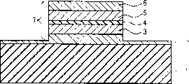
图1是本发明的磁阻元件的一例的剖视图;Fig. 1 is a cross-sectional view of an example of a magnetoresistive element of the present invention;
图2是本发明的磁阻元件的另一例的剖视图;2 is a cross-sectional view of another example of the magnetoresistive element of the present invention;
图3(a)~图3(c)表示本发明的磁阻元件一例中的磁特性和磁阻特性的图。3(a) to 3(c) are diagrams showing magnetic characteristics and magnetoresistance characteristics in an example of the magnetoresistive element of the present invention.
图4是表示利用本发明的元件的磁头的一例的图。FIG. 4 is a diagram showing an example of a magnetic head using the device of the present invention.
图5是利用本发明的元件的存储装置一例中的单元剖视图。Fig. 5 is a cross-sectional view of a cell in an example of a memory device using the device of the present invention.
具体实施方式Detailed ways
下面参照附图说明本发明的磁阻元件和利用这类元件的磁器件的优选实施例。DETAILED DESCRIPTION OF THE PREFERRED EMBODIMENTS Preferred embodiments of a magnetoresistive element and a magnetic device using such an element according to the present invention will be described below with reference to the accompanying drawings.
在图1所示的磁阻元件中,在基底1上依次层叠氮化钛(TiN)层2,光晶石型磁性层(第一磁性层)3,非磁性层4,第二磁性层5。在第二磁性层5上还配置电极6(上部电极)。用于检测外磁场的电流沿垂直于薄膜表面的方向流过两磁性层和非磁性层。In the magnetoresistive element shown in FIG. 1, a titanium nitride (TiN)
在上述元件中,氮化钛层处在形成光晶石型磁性层的整个区域上。如果这样夹入氮化钛层,可以确认,与没有该层时相比,磁阻变化可达二倍以上。其机理目前还不清楚。氮化钛具有晶格常数为4.24的岩盐型立方晶结构。该晶格常数相当于作为典型的光晶石型磁性体的四氧化三铁的立方晶结构的晶格常数8.4的大约一半。当然,对改善晶格特性有贡献的除结晶晶格的整合性以外还有其它重要因素。这是因为即使采用晶格接合良好的氧化镁(晶格常数为4.20,岩盐型立方结晶结构),MgAl2O4(晶格常数为8.1,光晶石型结晶结构)等基底,也不能获得象将氮化钛层介入的元件那样的高性能元件。除结晶晶格的整合性以外,还可能与例如在光晶石型磁性层与氮化钛层的界面上的包含电的化学的准位和稳定性的综合整合性有关。对氮化钛层的膜厚没有特别限定,但为了充分提高磁阻效应最好是50nm以上。In the above-mentioned element, the titanium nitride layer is on the entire region where the photonite type magnetic layer is formed. When the titanium nitride layer was interposed in this way, it was confirmed that the magnetoresistance change was more than double that of the case without the layer. Its mechanism is still unclear. Titanium nitride has a rock-salt type cubic crystal structure with a lattice constant of 4.24 Å. This lattice constant corresponds to about half of the lattice constant of 8.4 Å in the cubic crystal structure of ferric iron tetroxide, which is a typical optinite-type magnetic material. Of course, there are other important factors besides the integrity of the crystal lattice that contribute to the improvement of the lattice properties. This is because even with substrates such as magnesium oxide (lattice constant of 4.20 Å, rock-salt cubic crystal structure) and MgAl 2 O 4 (lattice constant of 8.1 Å, cartilite crystal structure) with good lattice bonding, the A high-performance element like an element in which a titanium nitride layer is interposed cannot be obtained. In addition to the integrity of the crystal lattice, it may also be related to, for example, the comprehensive integration of electrical, chemical potential and stability at the interface between the kangite-type magnetic layer and the titanium nitride layer. The film thickness of the titanium nitride layer is not particularly limited, but it is preferably 50 nm or more in order to sufficiently enhance the magnetoresistance effect.
虽然在用含铬、镍、锰的磁性体作为具有光晶石型结构的第一磁性层3的情况下,也能获得用氮化钛层改善特性的效果,但在利用含铁元素的氧化物铁磁体的情况下,也可以获得电特性和化学稳定性优良的磁阻元件。可获得最大磁阻变化的材料是二价铁和三价铁的复合价数氧化物四氧化三铁(Fe3O4)。Although in the case of using a magnetic body containing chromium, nickel, and manganese as the first magnetic layer 3 having a cartilite structure, the effect of improving the characteristics of the titanium nitride layer can also be obtained, but in the case of using an oxidizing element containing iron Even in the case of a ferromagnet, a magnetoresistive element excellent in electrical characteristics and chemical stability can be obtained. The material that can obtain the largest magnetoresistance change is triiron tetroxide (Fe 3 O 4 ), a composite valence oxide of ferrous iron and ferric iron.
业已确认在利用铜这样的良导体作为非磁性层4的情况(所谓CPP-GMR元件的情况)也可以得到如采用氮化钛层改善性能一样的效果。但是,在采用氧化物、氮化物等作为非磁性层的TMR元件中,将使磁阻效应显著增强。It has been confirmed that when a good conductor such as copper is used as the non-magnetic layer 4 (in the case of a so-called CPP-GMR element), the same performance-improving effect as when a titanium nitride layer is used can be obtained. However, in a TMR element using oxide, nitride, etc. as a nonmagnetic layer, the magnetoresistance effect will be remarkably enhanced.
虽然也可以利用玻璃这样的非晶形材料或多晶陶瓷作为基底1,但单晶材料最适合。因为利用单晶基底时,氮化钛的结晶方向容易大致朝一个方向,其结果也容易影响光晶石型磁性层的取向。Although an amorphous material such as glass or polycrystalline ceramics can also be used as the substrate 1, a single crystal material is most suitable. When a single crystal substrate is used, the crystallographic direction of titanium nitride tends to be roughly in one direction, and as a result, the orientation of the photonite-type magnetic layer tends to be affected.
虽然也可以用硅、兰宝石等作为单晶基底,但使用氧化镁的单晶能得到特别优良的效果,被认为是因为可以同时在氧化镁基底,氮化钛层和光晶石型磁性体层的两界面中实现结晶学和化学的高整合性。并且把基底的表面作为氧化镁结晶面(110)时,与在由(111)面和(211)面等组成的氧化镁表面上制作的情况下相比,可以得到良好的特性。另外在把基底表面作为(110)面的情况下,当把引起电阻变化的外磁场沿氧化镁的(110)方向形成45°角的方向加入时,可以得到大的磁阻变化率。如上所述,利用氮化钛和整合性高的基底,并在该基底上直接形成氮化钛层时,可以通过简单结构实现良好的接合。Although silicon, sapphire, etc. can also be used as a single crystal substrate, the use of a single crystal of magnesium oxide can achieve particularly good results. The high integration of crystallography and chemistry is achieved in the two interfaces of . In addition, when the surface of the substrate is the magnesia crystal plane (110), better characteristics can be obtained compared with the case where the magnesia surface is composed of (111) plane and (211) plane. In addition, when the surface of the substrate is used as the (110) plane, when the external magnetic field that causes the resistance change is added along the direction of the (110) direction of magnesium oxide forming a 45° angle, a large magnetoresistance change rate can be obtained. As described above, when titanium nitride is used and a substrate with high integrity is used, and a titanium nitride layer is directly formed on the substrate, good bonding can be achieved with a simple structure.
上面示出的氮化钛以外的各种材料是几个例子。对于用在第二磁性层5,电极6以及其它层上的材料没有特别限制,也可以使用过去一直使用的材料。对各层的成膜法也没有特殊限定,对氮化钛层的成膜法也不限定,例如可使用各种溅射法,化学气相沉积法(CVD)等。上述元件,是本发明的元件的一个例子,上述元件也可以制成包含图中没有示出的层,例如包括象抗强磁性层那种抑制磁性层的磁化回转的层的多层膜。在图示的结构中,通过把氮化钛层也作为下部电极使用,在基底1与第一磁性层3之间只夹入氮化钛层,当然,只要能达到本发明的目的也可以采用夹入其它层的结构。元件的形状也不限于图1中所例示。如图2所示也可以光刻技术等微细加工在器件上形成台阶部7。这种情况如图2所示,可以进行加工,以使作为电极的氮化钛层2残留在基底1上。Various materials other than titanium nitride shown above are a few examples. There are no particular limitations on the materials used for the second
在图4中示出了磁阻效应型磁头作为使用上述元件的磁传感器(sensor)的一个例子。在该磁头中,待检测的外磁场H通过由导磁率高的磁性膜构成的磁轭8加到磁阻元件9中,这时,虽然外磁场可以加到整个元件上,但也可以加到磁化回转相对容易的磁化层中。磁轭的材料可以用以前一直用的材料,例如可以用Fe-Si-Al,Co-Nb-Zr,Fe-Ta-N合金等软磁性膜,其形成方法也可以使用电镀等公知的成膜方法。A magnetoresistance effect type magnetic head is shown in FIG. 4 as an example of a magnetic sensor (sensor) using the above elements. In this magnetic head, the external magnetic field H to be detected is applied to the magnetoresistive element 9 through the yoke 8 made of a magnetic film with high magnetic permeability. At this time, although the external magnetic field can be applied to the entire element, it can also be added to In the magnetized layer where the magnetization reversal is relatively easy. The material of the yoke can be used in the past. For example, soft magnetic films such as Fe-Si-Al, Co-Nb-Zr, and Fe-Ta-N alloys can be used. The formation method can also use known film formation methods such as electroplating. method.
在图5中示出了利用上述元件构成磁存储器装置的一例。在该例中,如图2所示的磁阻元件的表面被绝缘层10覆盖,在该层上还层叠产生信息记录用磁场的导线11。在该单元中例如通过使电流在导线11中流过而产生磁场,使在初始状态中磁化方向一致的磁性层3、5中之一磁化反转。在图5中例示的元件中,由于第二磁性层5比第一磁性层3容易磁化回转,而显示第二磁性层5的磁化反转状态。这样,通过其中一个磁性层磁化反转后进行信息的记录。在该元件中,通过检测氮化钛层2与输出电极6之间的电阻变化读出信息。另外,作为导体11的材料也没有特别限定,可以采用Al、Au、Cu和Ag等低电阻导线。FIG. 5 shows an example of a magnetic memory device constructed using the above elements. In this example, the surface of the magnetoresistive element shown in FIG. 2 is covered with an insulating
在上面所述中只不过例示地说明器件构成和动作,本发明的元件可适用各种结构的磁器件。磁器件的动作例如也只列举了上述说明的存储器动作的一个例子。The above descriptions are merely illustrative of device configurations and operations, and the elements of the present invention are applicable to magnetic devices of various structures. The operation of the magnetic device is, for example, only an example of the operation of the memory described above.
实施例Example
实施例1Example 1
采用作为反光晶石型结晶构造的铁磁体的四氧化三铁(Fe3O4)磁性薄膜制作与图1同样结构的磁阻元件。用表面被无定形状态氧化硅(热氧化膜)覆盖的硅基底作为基底。在该基底上通过在把钛金属作为靶的氩/氮混合物气氛中溅射形成膜厚100nm的氮化钛(TiN)膜。其中,设定TiN膜成膜时基底温度为500℃。接着形成膜厚50nm的四氧化三铁磁性薄膜层。并在使铝的溅射膜附着2nm后氧化该膜,形成氧化铝膜作为绝缘层。接着形成膜厚20nm的CoFe强磁性层,最后形成金电极作为输出电极。A magnetoresistive element having the same structure as that in FIG. 1 was produced by using a ferromagnetic ferromagnetic thin film of iron tetraoxide (Fe 3 O 4 ) which is a reflective crystal structure. A silicon substrate whose surface was covered with silicon oxide (thermal oxide film) in an amorphous state was used as the substrate. A titanium nitride (TiN) film having a film thickness of 100 nm was formed on the substrate by sputtering in an argon/nitrogen mixture atmosphere using titanium metal as a target. Wherein, the substrate temperature is set at 500° C. when the TiN film is formed. Next, a ferroferromagnetic thin film layer with a film thickness of 50 nm was formed. And after attaching a sputtered film of aluminum to 2 nm, the film was oxidized to form an aluminum oxide film as an insulating layer. Next, a CoFe ferromagnetic layer with a film thickness of 20 nm was formed, and finally a gold electrode was formed as an output electrode.
测定这样获得的元件的电阻(TiN与金电极之间的电阻)随外磁场的变化关系,观测到约4%的电阻变化。与此相对应,在与上述同样方法制作的没有TiN层的元件中,电阻变化为1%以下。The resistance (resistance between TiN and gold electrodes) of the element thus obtained was measured against an external magnetic field, and a resistance change of about 4% was observed. On the other hand, in the element without the TiN layer fabricated by the same method as above, the resistance change was 1% or less.
另外,在与上述各层的层叠顺序相反在作为第二磁性层形成的四氧化三铁膜上形成TiN层的情况下,虽然得到了有效的特性提高的效果,但上述效果并不如与基底相邻地形成TiN层的情况。In addition, in the case where the TiN layer is formed on the ferric iron tetroxide film formed as the second magnetic layer in the reverse order of the stacking order of the above-mentioned layers, although an effective characteristic improvement effect is obtained, the above-mentioned effect is not as good as that of the base layer. The case where a TiN layer is adjacently formed.
实施例2Example 2
除用氧化镁单晶基底作为基底外,其它均按实施例1那样制作磁阻元件。把基底面设定为(100)面。当在TiN层的成膜过程中把基底的温度加热到300℃以上时,可获得TiN的<100>轴相对基底表面垂直取向的薄膜。另外,如果基底温度为室温~200℃左右,则变成具有多晶结构的TiN层。这两个TiN层呈金色,都是具有0.02mΩ·cm以下的电阻率的良导体。对这些元件的磁阻特性的评价表明,含多晶TiN层的元件的磁阻变化率为5%,与此相对,含<100>取向的TiN层的元件的磁阻变化率可达10%。A magnetoresistive element was manufactured in the same manner as in Example 1 except that a magnesium oxide single crystal substrate was used as a substrate. Set the base plane to the (100) plane. When the temperature of the substrate is heated to above 300°C during the formation of the TiN layer, a thin film with the <100> axis of TiN vertically oriented relative to the surface of the substrate can be obtained. In addition, if the substrate temperature is about room temperature to 200° C., it becomes a TiN layer having a polycrystalline structure. These two TiN layers are golden in color, and both are good conductors having a resistivity of 0.02 mΩ·cm or less. The evaluation of the magnetoresistance characteristics of these elements showed that the magnetoresistance change rate of the element containing the polycrystalline TiN layer was 5%, while the magnetoresistance change rate of the element containing the <100>-oriented TiN layer could reach 10% .
在用MnFe2O4、CoFe2O4等铁磁性层作为光晶石型磁性层的情况下,可以制作出显示8%左右的磁阻变化率的元件。另外若制作插入作为代替TiN层的良导体的白金(Pt)的取向膜的元件,磁阻变化率降到2%。When a ferromagnetic layer such as MnFe 2 O 4 or CoFe 2 O 4 is used as the optelite type magnetic layer, an element showing a magnetoresistance change rate of about 8% can be fabricated. In addition, when an element is manufactured in which an alignment film of platinum (Pt), which is a good conductor instead of the TiN layer, is inserted, the magnetoresistance change rate is reduced to 2%.
实施例3Example 3
利用具有(100)、(110)或(111)面方位的表面的MgO作为基底制作具有与图2同样构成的磁阻元件。首先把基底加热到400℃形成厚度为300nm的TiN层,接着依次层叠厚度为50nm的Fe3O4磁性层、厚度为1nm的氧化铝绝缘层、厚度为20nm的CoFe磁性层和厚度为100nm的铜电极层,结果确认到以下情况:在上述层叠工序中,TiN层与使用的基底表面相对应,上述基底分别大致垂直于轴<100><110>或<111>取向,Fe3O4磁性层也具有与TiN层同样的取向性。利用光刻和离子蚀刻等超精细加工,加工出具有台阶的台面式元件。把台面的图形制成边长为10000nm的正方形。A magnetoresistive element having the same configuration as in FIG. 2 was fabricated using MgO having a surface with a (100), (110) or (111) plane orientation as a base. First, the substrate is heated to 400°C to form a TiN layer with a thickness of 300nm, and then a Fe 3 O 4 magnetic layer with a thickness of 50nm, an aluminum oxide insulating layer with a thickness of 1nm, a CoFe magnetic layer with a thickness of 20nm, and a magnetic layer with a thickness of 100nm are sequentially stacked. Copper electrode layer, as a result, it was confirmed that the TiN layer corresponds to the surface of the substrate used in the above-mentioned lamination process, the above-mentioned substrate is approximately perpendicular to the axis <100><110> or <111> orientation, and Fe 3 O 4 magnetic The layer also has the same orientation as the TiN layer. Utilize ultra-fine processing such as photolithography and ion etching to process mesa elements with steps. The figure of the mesa is made into a square with a side length of 10000nm.
对这样制成的各元件,通过使TiN与铜电极之间流过电流检测磁阻变化。在图3(a)~(c)中示出了结果。虽然在用MgO(100)面的情况下可获得磁阻变化率约12%,在用MgO(111)面情况下可获得6%的磁阻变化率,但如利用MgO(110)面时,磁阻变化率超过20%。并且如沿MgO基底表面平行的<111>方向平行施加外磁场,可以使磁阻变化率达到最大。For each of the elements thus fabricated, a change in magnetoresistance was detected by passing a current between the TiN and copper electrodes. The results are shown in FIGS. 3( a ) to ( c ). Although about 12% of the magnetoresistance change rate can be obtained in the case of the MgO(100) surface, and 6% of the magnetoresistance change rate can be obtained in the case of the MgO(111) surface, but when using the MgO(110) surface, The magnetoresistance change rate exceeds 20%. And if the external magnetic field is applied parallel to the <111> direction parallel to the surface of the MgO substrate, the magnetoresistance change rate can be maximized.
(实施例4)(Example 4)
在本实施例中测定了磁阻变化率随着非磁性层种类的不同而异的情况。把MgO(110)面作为基底依次形成TiN层(300nm),下部Fe3O4磁性层(10nm)、绝缘层(2nm)、上部Fe3O4磁性层(20nm)。其中括弧内的数字是膜厚度。在TiN层成膜时,将基底加热到400℃。另外层叠膜厚50nm的LaFeO3层作为用于固定上部Fe3O4磁性层的磁化的抗强磁性层,最后从上部Fe3O4磁性层厚度为100nm的金输出电极。In this example, it was measured that the magnetoresistance change rate differs depending on the type of the nonmagnetic layer. The MgO(110) surface is used as the base to form a TiN layer (300nm), a lower Fe 3 O 4 magnetic layer (10nm), an insulating layer (2nm), and an upper Fe 3 O 4 magnetic layer (20nm). The numbers in parentheses are the film thicknesses. When the TiN layer is formed, the substrate is heated to 400°C. A LaFeO 3 layer with a thickness of 50 nm was laminated as an antiferromagnetic layer for fixing the magnetization of the upper Fe 3 O 4 magnetic layer, and finally a gold output electrode with a thickness of 100 nm was output from the upper Fe 3 O 4 magnetic layer.
分别用氧化铝、氧化钽、氧化钛、氧化镁、氧化铈、钛酸锶、氮化铝作为绝缘层。在MgO的<110>方向施加磁场,测定磁阻率变化,测定值在氧化钽、氧化镁、氮化铝的情况中为10%以下,在氧化钛,氧化锶的情况中为15%左右,在氧化铝的情况下为20%左右,在钛酸锶的情况下达到25%。虽然磁阻效应对绝缘阻挡层的材料的依赖原因尚不确定,但推测是绝缘阻挡层的元素对磁性层的电子状态的影响而致的。Aluminum oxide, tantalum oxide, titanium oxide, magnesium oxide, cerium oxide, strontium titanate, and aluminum nitride are respectively used as insulating layers. Apply a magnetic field in the <110> direction of MgO, and measure the change in magnetic resistivity. The measured value is 10% or less in the case of tantalum oxide, magnesium oxide, and aluminum nitride, and about 15% in the case of titanium oxide and strontium oxide. In the case of alumina, it is about 20%, and in the case of strontium titanate, it reaches 25%. Although the reason for the dependence of the magnetoresistance effect on the material of the insulating barrier layer is not certain, it is presumed to be due to the influence of the elements of the insulating barrier layer on the electronic state of the magnetic layer.
实施例5Example 5
利用按照实施例4制作的含钛酸锶绝缘层的元件制成与图4的构成相同的磁头。以大致从MgO(110)基底的<110>方位倾斜30°的方向施加由磁轭引导的磁场的方式,在上述磁头中配置磁轭以及元件,从而得到对零磁场附近的微弱磁场的良好灵敏度。其中,利用CoNbZr的无定形合金膜制作磁轭。由于附加上述那样配置的磁轭,而可以使该磁头对10(Oe)(约796A/m)的外磁场的灵敏度提高二倍以上。A magnetic head having the same configuration as that shown in FIG. 4 was produced by using the element containing a strontium titanate insulating layer fabricated according to Example 4. FIG. By arranging the yoke and elements in the above-mentioned magnetic head in such a way that the magnetic field guided by the yoke is applied in a direction inclined approximately 30° from the <110> orientation of the MgO(110) substrate, good sensitivity to a weak magnetic field near zero magnetic field is obtained . Among them, an amorphous alloy film of CoNbZr is used to make a magnetic yoke. By adding the yoke arranged as above, the sensitivity of the magnetic head to an external magnetic field of 10 (Oe) (about 796 A/m) can be doubled or more.
实施例6Example 6
制造具有图5所示的单元的存储装置。在以作为基底的MgO的(110)面上,依次层叠TiN层(800nm)、(Fe,Co)3O4磁性层(20nm)、氧化钛绝缘层(1nm)、CoFe磁性层(5nm)和铜电极层(100nm)(括弧内的数值为膜厚度)。接着进行微细加工,以使上述各层变成5000nm×2000nm尺寸的台面图形,用SiO2绝缘膜(300nm)覆盖整个表面。在该绝缘膜上配设由Al构成的信息记录用导线而制成存储单元。A memory device having the cell shown in FIG. 5 was fabricated. On the (110) plane of MgO as the base, TiN layer (800nm), (Fe, Co) 3 O 4 magnetic layer (20nm), titanium oxide insulating layer (1nm), CoFe magnetic layer (5nm) and Copper electrode layer (100nm) (the value in brackets is the film thickness). Next, microfabrication is carried out so that each of the above layers becomes a mesa pattern with a size of 5000nm×2000nm, and the entire surface is covered with a SiO 2 insulating film (300nm). An information recording wire made of Al was arranged on the insulating film to form a memory cell.
利用该存储单元进行信息的记录和再现。首先通过使脉动电流在信息记录用导线上流过而产生100(Oe)(约7960A/m)的磁场,使两磁性层方位一致。接着使脉冲电流沿相反方向流过而产生-50(Oe)(约-398A/m)的磁场,以仅使上部磁性层(CoFe磁性层)磁化反转。在该状态下,在TiN层与铜电极之间加电压,观测两电极之间的电阻变化,可以测定出明显的电阻变化。Recording and reproduction of information are performed using this storage unit. First, a magnetic field of 100 (Oe) (approximately 7960 A/m) was generated by passing a pulsating current through an information recording wire, so that the orientations of the two magnetic layers were aligned. Next, a pulse current was passed in the opposite direction to generate a magnetic field of -50 (Oe) (about -398 A/m) to reverse the magnetization of only the upper magnetic layer (CoFe magnetic layer). In this state, a voltage is applied between the TiN layer and the copper electrode, and the resistance change between the two electrodes is observed, and a significant resistance change can be measured.
如上所述,按照本发明可以提供利用高自旋极化率光晶石型磁性材料的磁阻效应大的磁阻元件。该元件的制造也容易。本发明的技术方案能够方便地批量生产具有优良特性的磁传感器和磁阻效应型存储装置,在该技术领域具有极大的利用价值。As described above, according to the present invention, it is possible to provide a magnetoresistance element having a large magnetoresistance effect using a photoparite type magnetic material with a high spin polarizability. The element is also easy to manufacture. The technical scheme of the invention can conveniently mass-produce magnetic sensors and magnetoresistance effect storage devices with excellent characteristics, and has great utilization value in this technical field.
Claims (12)
Applications Claiming Priority (3)
| Application Number | Priority Date | Filing Date | Title |
|---|---|---|---|
| JP2000292035A JP3603771B2 (en) | 2000-09-26 | 2000-09-26 | Magnetic resistance element, magnetic sensor and memory device using the same |
| JP292035/00 | 2000-09-26 | ||
| JP292035/2000 | 2000-09-26 |
Publications (2)
| Publication Number | Publication Date |
|---|---|
| CN1346156A CN1346156A (en) | 2002-04-24 |
| CN1211873C true CN1211873C (en) | 2005-07-20 |
Family
ID=18775033
Family Applications (1)
| Application Number | Title | Priority Date | Filing Date |
|---|---|---|---|
| CNB011372362A Expired - Fee Related CN1211873C (en) | 2000-09-26 | 2001-09-26 | Magnetic resistance element and magnetic device using same |
Country Status (5)
| Country | Link |
|---|---|
| US (1) | US6639765B2 (en) |
| EP (1) | EP1191344A3 (en) |
| JP (1) | JP3603771B2 (en) |
| KR (1) | KR100439143B1 (en) |
| CN (1) | CN1211873C (en) |
Families Citing this family (26)
| Publication number | Priority date | Publication date | Assignee | Title |
|---|---|---|---|---|
| JP3854836B2 (en) * | 2001-09-28 | 2006-12-06 | キヤノン株式会社 | Design method of magnetic memory using perpendicular magnetization film |
| US6897532B1 (en) * | 2002-04-15 | 2005-05-24 | Cypress Semiconductor Corp. | Magnetic tunneling junction configuration and a method for making the same |
| WO2003092083A1 (en) * | 2002-04-24 | 2003-11-06 | Matsushita Electric Industrial Co., Ltd. | Magnetoresistant element |
| US7428127B2 (en) * | 2002-12-24 | 2008-09-23 | Fujitsu Limited | CPP magnetoresistive effect element and magnetic storage device having a CPP magnetoresistive effect element |
| KR100512180B1 (en) | 2003-07-10 | 2005-09-02 | 삼성전자주식회사 | Magnetic tunnel junction in magnetic random access memory device and method for forming the same |
| WO2005101420A1 (en) * | 2004-04-16 | 2005-10-27 | Matsushita Electric Industrial Co. Ltd. | Thin film memory device having a variable resistance |
| WO2005106955A1 (en) * | 2004-04-27 | 2005-11-10 | Matsushita Electric Industrial Co., Ltd. | Storage element |
| KR100695135B1 (en) * | 2004-12-17 | 2007-03-14 | 삼성전자주식회사 | Magnetoresistive element using TiN as top layer |
| JP2007165449A (en) * | 2005-12-12 | 2007-06-28 | Tdk Corp | Magnetic storage device |
| WO2007086325A1 (en) * | 2006-01-24 | 2007-08-02 | Matsushita Electric Industrial Co., Ltd. | Electric element, memory device and semiconductor integrated circuit |
| JP4699932B2 (en) * | 2006-04-13 | 2011-06-15 | パナソニック株式会社 | Resistance change element, resistance change memory using the same, and manufacturing method thereof |
| KR100851891B1 (en) * | 2006-12-15 | 2008-08-13 | 한국과학기술연구원 | Multilayer structure having high spin injection ratio using conductive nitride as a spacer |
| KR101219774B1 (en) * | 2007-07-20 | 2013-01-18 | 삼성전자주식회사 | Method of forming semiconductor device having transition metal oxide layer and related device |
| JP4649457B2 (en) * | 2007-09-26 | 2011-03-09 | 株式会社東芝 | Magnetoresistive element and magnetic memory |
| US8368175B2 (en) | 2008-03-28 | 2013-02-05 | Nec Corporation | Capacitor, semiconductor device having the same, and method of producing them |
| KR100884610B1 (en) * | 2008-07-18 | 2009-02-23 | 한국과학기술연구원 | Multi-layered film structure having high spin injection efficiency using conductive nitride as interlayer and method for manufacturing same |
| JP4978868B2 (en) * | 2008-11-20 | 2012-07-18 | 独立行政法人科学技術振興機構 | Spin filter effect element and magnetic device using the same |
| US9379315B2 (en) * | 2013-03-12 | 2016-06-28 | Micron Technology, Inc. | Memory cells, methods of fabrication, semiconductor device structures, and memory systems |
| US9529060B2 (en) * | 2014-01-09 | 2016-12-27 | Allegro Microsystems, Llc | Magnetoresistance element with improved response to magnetic fields |
| US9633866B2 (en) * | 2015-05-18 | 2017-04-25 | Texas Instruments Incorporated | Method for patterning of laminated magnetic layer |
| JP6724646B2 (en) * | 2016-08-10 | 2020-07-15 | Tdk株式会社 | Magnetoresistive element, thermal history sensor and magnetic memory using spin glass |
| JP6103123B1 (en) * | 2016-09-02 | 2017-03-29 | Tdk株式会社 | Magnetoresistive element, magnetic sensor and magnetic memory |
| US10908234B2 (en) | 2016-09-02 | 2021-02-02 | Tdk Corporation | Magnetoresistance effect element, magnetic sensor and magnetic memory |
| JP2018056388A (en) * | 2016-09-29 | 2018-04-05 | Tdk株式会社 | Magnetoresistive effect element |
| EP3811073A4 (en) * | 2018-06-22 | 2022-06-29 | Magarray, Inc. | Magnetic sensors with a mixed oxide passivation layer |
| US11953742B2 (en) * | 2021-03-30 | 2024-04-09 | Tdk Corporation | Optical device and optical system |
Family Cites Families (11)
| Publication number | Priority date | Publication date | Assignee | Title |
|---|---|---|---|---|
| JPH01208714A (en) * | 1988-02-16 | 1989-08-22 | Nec Kansai Ltd | Magneto-resistance effect type magnetic head and its manufacture |
| JP2560482B2 (en) * | 1989-08-04 | 1996-12-04 | 日本電気株式会社 | Magnetoresistive head |
| WO1993011569A1 (en) | 1991-12-03 | 1993-06-10 | Nippondenso Co., Ltd. | Magnetoresistant element and manufacturing process thereof |
| US5485333A (en) * | 1993-04-23 | 1996-01-16 | Eastman Kodak Company | Shorted DMR reproduce head |
| JPH0935216A (en) * | 1995-07-21 | 1997-02-07 | Hitachi Ltd | Magnetoresistance effect film and magnetic recording head |
| US5835003A (en) * | 1995-09-29 | 1998-11-10 | Hewlett-Packard Company | Colossal magnetoresistance sensor |
| US5712612A (en) * | 1996-01-02 | 1998-01-27 | Hewlett-Packard Company | Tunneling ferrimagnetic magnetoresistive sensor |
| KR20010013595A (en) * | 1997-06-09 | 2001-02-26 | 엔, 마이클 그로브 | Annealing of a crystalline perovskite ferroelectric cell and cells exhibiting improved barrier properties |
| US6169688B1 (en) * | 1998-03-23 | 2001-01-02 | Kabushiki Kaisha Toshiba | Magnetic storage device using unipole currents for selecting memory cells |
| US6313973B1 (en) * | 1998-06-30 | 2001-11-06 | Kabushiki Kaisha Toshiba | Laminated magnetorestrictive element of an exchange coupling film, an antiferromagnetic film and a ferromagnetic film and a magnetic disk drive using same |
| JP2000174359A (en) | 1998-12-09 | 2000-06-23 | Toshiba Corp | Magnetoresistive element |
-
2000
- 2000-09-26 JP JP2000292035A patent/JP3603771B2/en not_active Expired - Fee Related
-
2001
- 2001-09-25 US US09/963,895 patent/US6639765B2/en not_active Expired - Lifetime
- 2001-09-26 CN CNB011372362A patent/CN1211873C/en not_active Expired - Fee Related
- 2001-09-26 EP EP01308169A patent/EP1191344A3/en not_active Withdrawn
- 2001-09-26 KR KR10-2001-0059686A patent/KR100439143B1/en not_active IP Right Cessation
Also Published As
| Publication number | Publication date |
|---|---|
| EP1191344A3 (en) | 2004-07-07 |
| US6639765B2 (en) | 2003-10-28 |
| KR100439143B1 (en) | 2004-07-05 |
| JP2002111094A (en) | 2002-04-12 |
| CN1346156A (en) | 2002-04-24 |
| JP3603771B2 (en) | 2004-12-22 |
| EP1191344A2 (en) | 2002-03-27 |
| KR20020024807A (en) | 2002-04-01 |
| US20020036315A1 (en) | 2002-03-28 |
Similar Documents
| Publication | Publication Date | Title |
|---|---|---|
| CN1211873C (en) | Magnetic resistance element and magnetic device using same | |
| KR101457511B1 (en) | Spin hall effect magnetic apparatus, method and applications | |
| KR100245066B1 (en) | Thin film magnetoresistive element | |
| US6347049B1 (en) | Low resistance magnetic tunnel junction device with bilayer or multilayer tunnel barrier | |
| US6153320A (en) | Magnetic devices with laminated ferromagnetic structures formed with improved antiferromagnetically coupling films | |
| US7443639B2 (en) | Magnetic tunnel junctions including crystalline and amorphous tunnel barrier materials | |
| US7349187B2 (en) | Tunnel barriers based on alkaline earth oxides | |
| US8513944B2 (en) | Three-layer magnetic element, magnetic field sensor, magnetic memory and magnetic logic gate using such an element | |
| US7300711B2 (en) | Magnetic tunnel junctions with high tunneling magnetoresistance using non-bcc magnetic materials | |
| US20040041183A1 (en) | Amorphous alloys for magnetic devices | |
| JP2004524708A (en) | Magnetoresistive element, magnetoresistive magnetic head using the same, magnetic recording device, and magnetoresistive memory device | |
| WO2002099905A1 (en) | Tunnel magnetoresistance element | |
| WO2004059745A1 (en) | Magnetic switching device and magnetic memory | |
| JP2013165295A (en) | Magnetoresistive magnetic field sensor | |
| JP6857421B2 (en) | Ferromagnetic tunnel junction, spintronics device using it, and method for manufacturing ferromagnetic tunnel junction | |
| JP3593472B2 (en) | Magnetic element, magnetic memory and magnetic sensor using the same | |
| JP2004179219A (en) | Magnetic device and magnetic memory using the same | |
| WO2005060657A2 (en) | Magnetoelectronic devices based on colossal magnetoresistive thin films | |
| JP3344712B2 (en) | Pinning layer for magnetic devices | |
| JP3578721B2 (en) | Magnetic control element, magnetic component and memory device using the same | |
| JP2005019484A (en) | Magnetoresistive effect element and magnetic head | |
| JP4039656B2 (en) | Exchange coupling element and method of manufacturing exchange coupling element | |
| CN116896980A (en) | Spin valve device with noble metal-free antiferromagnetic in the stabilization layer | |
| JP2002299725A (en) | Magnetoresistive device | |
| JP2907805B1 (en) | Magnetoresistive element, magnetoresistive head and magnetic recording / reproducing device |
Legal Events
| Date | Code | Title | Description |
|---|---|---|---|
| C06 | Publication | ||
| PB01 | Publication | ||
| C10 | Entry into substantive examination | ||
| SE01 | Entry into force of request for substantive examination | ||
| C14 | Grant of patent or utility model | ||
| GR01 | Patent grant | ||
| C17 | Cessation of patent right | ||
| CF01 | Termination of patent right due to non-payment of annual fee |
Granted publication date: 20050720 Termination date: 20100926 |