CN1198445C - Image processing method and image processor - Google Patents
Image processing method and image processor Download PDFInfo
- Publication number
- CN1198445C CN1198445C CN03136925.1A CN03136925A CN1198445C CN 1198445 C CN1198445 C CN 1198445C CN 03136925 A CN03136925 A CN 03136925A CN 1198445 C CN1198445 C CN 1198445C
- Authority
- CN
- China
- Prior art keywords
- pixel
- view data
- mentioned
- interpolation
- obtains
- Prior art date
- Legal status (The legal status is an assumption and is not a legal conclusion. Google has not performed a legal analysis and makes no representation as to the accuracy of the status listed.)
- Expired - Fee Related
Links
Images


Classifications
-
- H—ELECTRICITY
- H04—ELECTRIC COMMUNICATION TECHNIQUE
- H04N—PICTORIAL COMMUNICATION, e.g. TELEVISION
- H04N1/00—Scanning, transmission or reproduction of documents or the like, e.g. facsimile transmission; Details thereof
- H04N1/04—Scanning arrangements, i.e. arrangements for the displacement of active reading or reproducing elements relative to the original or reproducing medium, or vice versa
- H04N1/19—Scanning arrangements, i.e. arrangements for the displacement of active reading or reproducing elements relative to the original or reproducing medium, or vice versa using multi-element arrays
- H04N1/191—Scanning arrangements, i.e. arrangements for the displacement of active reading or reproducing elements relative to the original or reproducing medium, or vice versa using multi-element arrays the array comprising a one-dimensional array, or a combination of one-dimensional arrays, or a substantially one-dimensional array, e.g. an array of staggered elements
- H04N1/192—Simultaneously or substantially simultaneously scanning picture elements on one main scanning line
- H04N1/193—Simultaneously or substantially simultaneously scanning picture elements on one main scanning line using electrically scanned linear arrays, e.g. linear CCD arrays
Abstract
An image processing apparatus for processing image data, obtained from an image sensing unit in which plural sensor chips each having plural pixels are arrayed with an interval of a multiple of a pixel width therebetween, and interpolating image data for the interval. If an abnormal pixel exists, image data of the abnormal pixel is replaced with data in accordance with image data of a pixel adjacent to the abnormal pixel, and thereafter, interpolation is performed for the interval by using image data from a sensor chip adjacent to said interval.
Description
Technical field
The present invention relates to image processing method and image processing apparatus, particularly the image processing method and the image processing apparatus of the view data that obtains from the image capture unit of arranging a plurality of sensor chips and forming of processing.
Background technology
In the past, in digital copier etc., there was the contact-type image sensor (CIS) that uses a plurality of sensor chips that are connected in series to read the view data of 1 row to carry out the digital copier that original copy reads.Such CIS disposes on circuit board and is connected a plurality of sensor chips formations, but in present chip mounting technology, the pixel separation of sensor chip seam portion is greater than the pixel pitch in each sensor chip.Therefore, will change, particularly have when reading the original copy that site etc. has the cycle problem of generation striped on the image in the sampling period of the image of seam portion.
Because along with the progress of high-resolutionization, the pixel pitch of sensor chip becomes more and more littler, so the problems referred to above are the problems that must take place before the chip mounting technology is improved.
For this problem, well-known have a following method, promptly when connecting sensor chip, connect and make when chip assembles, to have surplus by physically leaving intended pixel ground, and then use multiply by the predetermined data that weight coefficient generated respectively from the output of the last pixel of sensor chip with from the output of the initial pixel of the sensor chip of adjacency, this leaves the pixel of intended pixel interpolation.
But, if exist unusual in the output of carrying out the above-mentioned interpolation surrounding pixel of sensor chip seam portion when handling, then when interpolation is handled, just use unusual data, thereby had the problem that to carry out normal interpolation processing and enlarge the abnormal data part.
Summary of the invention
The present invention finishes in view of the above problems, even if purpose is arranging the view data that the image capture unit of a plurality of sensor chips obtains and have abnormal data from separating predetermined space, also abutment joint portion carries out interpolation more naturally.
In order to achieve the above object, the invention provides a kind of image processing method, the view data that the image capture unit that processing forms from a plurality of sensor chips of the arranged spaced that separates the intended pixel amount obtains, described sensor chip has a plurality of pixels, it is characterized in that, may further comprise the steps: the abnormal pixel that detects the sensor chip; With obtain according to the pixel pixel value that is positioned at the both sides of above-mentioned abnormal pixel view data replace the view data of above-mentioned abnormal pixel; After the view data of the above-mentioned abnormal pixel of displacement, the pixel data of using the pixel value by the pixel around the average interval between the sensor chip to obtain, the view data at the corresponding above-mentioned interval of interpolation.
In addition, in order to achieve the above object, the present invention also provides the image processing apparatus of the view data that a kind of processing obtains from the image capture unit that a plurality of sensor chips with a plurality of pixels of the arranged spaced that separates the intended pixel amount form, it is characterized in that, comprising: the abnormal pixel checkout gear that detects the abnormal pixel of the sensor chip; Use based at the pixel pixel value of the both sides of above-mentioned abnormal pixel and the view data that obtains, replace the 1st interpolation device of the view data of above-mentioned abnormal pixel; And after the view data of the above-mentioned abnormal pixel of replacing above-mentioned the 1st interpolation device, with the view data that the pixel value by the pixel around the average interval between the sensor chip obtains, the 2nd interpolation device of the view data at the corresponding above-mentioned interval of interpolation.
Other features of the present invention and advantage are by coming to understand as the following explanation of reference with accompanying drawing.Here, in the accompanying drawings, additional identical with reference to label to identical or same structure.
Description of drawings
Accompanying drawing is included in the specification, constitutes its part, represents form of implementation of the present invention, and is used from explanation principle of the present invention with the record one of specification.
Fig. 1 is the figure of schematic configuration of the digital scanner of expression the 1st form of implementation of the present invention.
Fig. 2 is the simple structure chart of the contact-type image sensor of the 1st form of implementation of the present invention.
Fig. 3 is the enlarged drawing of the seam portion between expression CCD shown in Figure 2.
Fig. 4 A and Fig. 4 B are the figure that expression is used to illustrate the problem when having read image by contact-type image sensor shown in Figure 2.
Fig. 5 is the block diagram of control structure of the digital scanner of expression the 1st form of implementation of the present invention.
Fig. 6 A is the figure of structure of the contact-type image sensor of expression the present invention the 1st form of implementation.
Fig. 6 B is the figure of expression from the relation of the signal value that contact-type image sensor obtained of the present invention's the 1st form of implementation and main scanning direction position.
Fig. 7 A and Fig. 7 B are the figure of the notion handled of the interpolation of explanation the 1st form of implementation of the present invention.
Fig. 8 A and Fig. 8 B are the figure of the notion handled of the interpolation of explanation the 1st form of implementation of the present invention.
Fig. 9 A and Fig. 9 B are the figure of the notion handled of the interpolation of explanation the 1st form of implementation of the present invention.
Figure 10 is the figure of detection of the abnormal pixel position of explanation the present invention the 1st form of implementation.
Figure 11 A and Figure 11 B are the figure of the notion handled of the interpolation of explanation the 1st form of implementation of the present invention.
Figure 12 A and Figure 12 B are the figure of the notion handled of the interpolation of explanation the 1st form of implementation of the present invention.
Figure 13 A and Figure 13 B are the figure of the notion handled of the interpolation of explanation the 1st form of implementation of the present invention.
Figure 14 A and Figure 14 B are the figure of the notion handled of the interpolation of explanation the 1st form of implementation of the present invention.
Figure 15 is that the image of expression the present invention the 1st form of implementation reads and the flow chart of the interpolation treatment step of pixel data.
Figure 16 is the flow chart of the abnormal pixel treatment for correcting step of expression the present invention the 1st form of implementation.
Figure 17 is the figure that is used to illustrate the shading correction of the present invention's the 2nd form of implementation.
Embodiment
Below, the preferred implementing form that present invention will be described in detail with reference to the accompanying.
<the 1 form of implementation 〉
Expression uses the contact-type image sensor of the present invention's the 1st form of implementation to read the structure chart of the general digital scanner of original copy among Fig. 1.On contact-type image sensor (CIS) unit 102, dispose contact-type image sensor (CIS) 101 and lamp 106.CIS unit 102 is connected with motor 104 by lead 108, and position transducer 107 indicates the original position of this CIS unit 102, by being that benchmark just changes, reverse motors 104 with this original position, and the whole read range that CIS unit 102 can scan manuscript table glass 103.
When reading the original copy 100 that is positioned on the manuscript table glass 103, with lamp 106 irradiation original copys 100, on one side in read range mobile CIS unit 102 read original copy 100 by CIS101 on one side.This reads action and is the document board read mode.
In addition, on the digital scanner of this 1st form of implementation, be equipped with master copy automatic conveying device (below abbreviation it " ADF ") 109, CIS unit 102 by motor 104 move and stop at air roll 113 under, can be under the state that stops with lamp 106 irradiations and read the original copy of being carried by conveying roller 112 100.If reading action, this is the ADF read mode.
As for being to use any read mode, can change by user's indication.
Fig. 2 is the simple structure chart of CIS101.
CIS101 for example arranges 5 CCD201 that have 1500 pixels respectively and constitutes, and can read the original copy of A4 by 600dpi.By utilizing the synthetic output of image processing circuit described later to form image from these 5 CCD201.In addition, Biao Shi pixel count and resolution are an example here, and self-evident the present invention is not limited only to this.
Fig. 3 is the figure that has amplified the seam portion of the CCD201 in the CIS101 of Fig. 2,202 each pixels of expression.In this 1st form of implementation, establish and connect so that be a pixel wide (about 0.0423mm) between the pixel 202L of the leftmost side of the pixel 202R of the rightmost side of CCD201 and the CCD201 that is adjacent.When read image such shown in Fig. 4 A (get can with 2 sizes that CCD201 reads of adjacency) by CIS101 with said structure, and when showing image shown in the resulting signal, just obtain shown in Fig. 4 B, to have lost like that the factitious image of a pixel of corresponding seam portion.Come the such pixel of losing of interpolation will improve its not naturality by image processing circuit described later.
Fig. 5 is the block diagram that the control of the digital scanner of expression the 1st form of implementation of the present invention constitutes.Here, to additional identical with the same formation of Fig. 1 with reference to label and omit its explanation.
In Fig. 5, the 501st, the A/D translation circuit that the output signal of CIS101 is carried out the A/D conversion, the 502nd, accept from the output of A/D translation circuit 501 and carry out the image processing circuit of the image processing etc. of shading correction, seam portion, the 503rd, detect the abnormal pixel testing circuit of the abnormal pixel in the CIS101, the 504th, when detecting abnormal pixel according to the abnormal pixel correcting circuit of this abnormal pixel of the normal pixel adjustment of data around it.The processing of abnormal pixel testing circuit 503 and abnormal pixel correcting circuit 504 was carried out before the processing that utilizes image processing circuit 502 to carry out.In addition, the 506th, accept to select the mode initialization of ADF read mode or document board read mode and begin to read the operating portion of the indication of original copy from the user.The 507th, the scanner controller, be used for each structure in the control figure scanner, for example, carry out according to the coding output of the encoder 505 that is equipped with from motor 104 with from the position that the output signal of position transducer 107 is held CIS unit 102, the output signal value that perhaps receives the CIS101 that was handled by image processing circuit 502 also sends this output signal to the control of external device (ED)s such as PC or printer (not having to illustrate) etc.
Then, the action to the image processing of the seam portion that comprises CIS101 in having the digital scanner of above-mentioned formation describes with reference to the flow chart of Figure 15 and Figure 16.
At first, in step S1501, judge by the specified read mode of operating portion 506.In step S1502 and S1503, read original copy 100 by specified read mode respectively, enter step S1504.
In step S1504, utilize the detection of the abnormal pixel of abnormal pixel testing circuit 503, in step S1505, utilize the correction of the abnormal pixel of abnormal pixel correcting circuit 504, to at length narrate in the back about these processing, at first, the interpolation of the seam portion of the view data that is read of carrying out in step S1506 and S1507 is handled described.
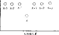
As the illustrated mistake of reference Fig. 2, owing in this 1st form of implementation, know the CCD201 chip that has adopted 5 to have 1500 pixels respectively in advance, so such as shown in Figure 6A, the seam portion 601 of the CCD201 in the CIS101 has 4 places every each pixel of 1500 pixels as can be known.The figure of the dateout of the main scanning direction position when Fig. 6 B is the original copy of expression a kind of color (for example white) of having read 1 row amount corresponding to the CIS101 that utilizes Fig. 6 A, the position of representing with circle is the data of corresponding seam portion 601.
Like this, because 2 CCD201 of adjacency are that arrange at the interval that separates 1 pixel size, so as described above, for example, when reading the image shown in Fig. 4 A and exporting signal from each pixel output of CCD201 unchangeably, just shown in Fig. 4 B, become factitious image like that with former states such as PC or printers.
In this 1st form of implementation, image processing circuit 502 becomes more natural image in order to make this factitious image, at first inserts the pseudo-data D (step S1506) of arbitrary value in seam portion.Fig. 7 A is the figure that is illustrated in the image when having inserted pseudo-data D among Fig. 4 B, and Fig. 7 B is the figure that is illustrated among Fig. 7 A with the dateout of the part 701 that thick frame surrounded.After pseudo-data D inserts, use pixel X-2, X-1, X+1, the X+2 on every side of seam portion to carry out, and replace pseudo-data D (step S1507) with this result of calculation as shown in the formula such weighted calculation shown in (1).Example when Fig. 8 A and Fig. 8 B have represented to replace pseudo-data D.Here, X-2, X-1, X+1, the X+2 of expression formula (1) represent the pixel value of pairing pixel.
X=a(X-2)+b(X-1)+c(X+1)+d(X+2) …(1)
Wherein, a+b+c+d=1
Like this, by using the result permutation seam portion that the data of surrounding pixel has been carried out weighted calculation, just can generate more natural image.
Here, although in this 1st form of implementation is will the data of 2 pixels of all directions have been carried out the result of weighted calculation as replacement data, but utilize the simple mean value of pixel X-1 and X+1 to replace, perhaps further use on all directions the above pixel values of 3 pixels to be weighted calculating and also can expect same effect.
Then, the action to abnormal pixel testing circuit 503 among step S1504 and the S1505 and abnormal pixel correcting circuit 504 describes.
In the ADF read mode; because what adopt is by carrying original copy 110 to come the formation of reading images under the state that has stopped CIS101; so on manuscript table glass 103 read the position adhered to grit or dust, when dirty etc.; CIS101 will read that these are dirty, will show striped on image.Fig. 9 A is illustrated in the figure that reads the example of the resulting image of image shown in Fig. 4 A when having grit etc., and Fig. 9 B is the figure of expression with the dateout of the part 901 that thick frame enclosed.
These grits etc. become white by making air roll 113 in advance, read and carry out binaryzation by predetermined threshold value with CIS101, as shown in Figure 10 the detection position.Like this, abnormal pixel testing circuit 503 detects the position of the abnormal pixel of the influence that is subjected to grit etc. in step S1504.
In step S1505, in order to proofread and correct abnormal pixel, abnormal pixel correcting circuit 504 receives the grit positional information according to the binaryzation result of abnormal pixel testing circuit 503.Shown in Fig. 9 A and Fig. 9 B like that, under the situation of the grit that has continuous 4 pixels, 2 pixels such as the left side of 4 pixels of corresponding grit etc. from the left side, 2 pixels on right side from the right side like that, utilize the data of the pixel of having used both sides to replace.Represent the result that replaced among Figure 11 A and Figure 11 B.
Like this, detect the data of pixel of data replacement grit part of pixel of the both sides of grit by use, just can generate more natural image.
But, under the situation that detects continuous 10 grits more than the pixel etc. with abnormal pixel testing circuit 503 (is YES at step S1601), even if also still can residual not naturality owing in thin especially literal, lines etc., carry out this treatment for correcting, so (step S1603) former state is not constant it is outputed to PC etc. with carrying out treatment for correcting, make the user recognize the situation of unusual generation.
Here, when considering before this abnormal pixel is proofreaied and correct, to carry out seam portion timing, then exist under the situation of grit such shown in Figure 12 B in position such shown in Figure 12 A, if the threshold value that the maximum of the weighting parameters A=B=C=D=0.25 of seam portion, read value is 100, grit detects is 50, under the situation of (X-3)=0, (X-2)=0, (X-1)=100, (X+1)=0, (X+2)=100, the data X=75 of seam portion.At this moment, the influence of grit is embodied in the data X of seam portion, owing to being that 50 former can not detections are grit in abnormal pixel test section threshold value, will produce striped on image.At this moment, the image that the image of Fig. 4 A is exported, the data of the position of the corresponding main scanning direction of the part 1201 that the thick frame of usefulness of presentation graphs 13A is surrounded in Figure 13 B are read in expression in Figure 13 A.
Thus, abnormal pixel treatment for correcting (step S1505) need (step S1506 and S1507) be carried out before the displacement of seam portion.Figure 14 A and Figure 14 B have represented to carry out in this order the result who handles.
Like this, in the digital scanner of this 1st form of implementation, owing to be to deploy in seam to carry out abnormal pixel before changing and proofread and correct, thus even if be subjected in existence under the situation of abnormal pixel of influence of grit etc., also can interior plug joint portion to become more natural image.
<the 2 form of implementation 〉
Below, the 2nd form of implementation of the present invention is described.Because the structure of the digital scanner of the 2nd form of implementation is identical with the 1st form of implementation, so omit its explanation here.In this 2nd form of implementation, just the data behind the shading correction are carried out the action of seam deployment when changing processing, abnormal pixel treatment for correcting and describe.
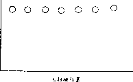
Figure 17 is the figure of the data output that obtained from CIS101 when having shone uniform white original copy of indication lamp 106, and it becomes the benchmark output in each position of main scanning direction.Usually because of the difference of lamp itself, the sensitivity difference etc. of pixel in the CCD201, this value is inconsistent to each pixel.
Thereby, be applied to each pixel by shading correction with following formula (2) expression, proofread and correct feasible output unanimity.
Dout=T/Dinw×Din …(2)
Desired value when T=reads the even benchmark original copy of white
Pixel output when Dinw=reads the even benchmark original copy of white
The Din=reading of data
Pixel data behind the Dout=shading correction
As described above, keep this pixel output and carry out above-mentioned treatment for correcting, just can proofread and correct feasible output unanimity by the even benchmark original copy that before reading original copy, reads white.
Owing to deploy in seam and to change in the processing to be generated, the interpolative data of seam portion is, for example surrounding pixel is weighted the simulation generation data that calculating obtains by following formula (1), so in order to carry out correct shading correction, value in the time of just need be to the even benchmark original copy of white is also used the weighted calculation of surrounding pixel, and it is complicated that the image processing structure will become.Thereby, need deploy and to carry out shading correction before changing processing, abnormal pixel treatment for correcting carrying out seam.
Although in the above-mentioned the 1st and the 2nd form of implementation, be after detecting the abnormal pixel position and having carried out the abnormal pixel treatment for correcting, carry out the displacement of seam portion, self-evidently when being connected in series a plurality of face sensor, also can obtain same effect.
<other forms of implementation 〉
In addition, the present invention also goes for the system by a plurality of equipment (for example main frame, interface equipment, scanner, video camera, printer etc.) formation, also go for the device (for example, scanner, photocopier, facsimile machine device etc.) that forms by individual equipment.
Need not superfluous words in addition, purpose of the present invention also can reach like this, the storage medium of the software program code by will having write down the function that realizes above-mentioned form of implementation (for example offers computer system or device exactly, personal computer), this system or device utilize CPU or MPU to read and carry out the program code that is kept in the storage medium.
In this case, just become the program code of reading from storage medium self will realize the function of above-mentioned form of implementation, the storage medium of storing this program code has just constituted the present invention.
In addition,, for example can use the storage medium of floppy disk, hard disk, CD, magneto optical disk, CD-ROM, CD-R, tape, Nonvolatile memory card and ROM etc., the perhaps computer network of LAN (local area network (LAN)) and WAN (wide area network) etc. for program code is provided.
Need not superfluous words in addition, not only comprise the program code of reading by object computer, the situation that the function of above-mentioned form of implementation is achieved, also comprise indication according to this program code, Yun Hang OS (operating system) etc. carries out part or all of actual treatment on computers, the situation that the function by this said form of implementation in processing front is achieved.
And then need not superfluous words, also comprise the program code of reading when from storage medium, be written to the function expansion card that inserts computer and/or be connected to after the memory that is possessed on the functional expansion unit of computer, indication according to this program code, the CPU that is possessed on this function expansion card and/or the functional expansion unit etc. carries out part or all of actual treatment, the situation that the function by this said form of implementation in processing front is achieved.
Be applicable in the present invention under the situation of above-mentioned storage medium, just be kept in this storage medium with Figure 15 illustrated in form of implementation and flow chart corresponding programs code shown in Figure 16.
The present invention is not limited to above-mentioned form of implementation, can carry out various changes and correction without departing from the spirit and scope of the present invention.Therefore, in order to disclose scope of the present invention, additional following claim item.
Claims (12)
1. an image processing method is handled the view data that obtains from the image capture unit that a plurality of sensor chips of the arranged spaced that separates the intended pixel amount form, and described sensor chip has a plurality of pixels, it is characterized in that, may further comprise the steps:
Detect the abnormal pixel of the sensor chip;
The view data that obtains with the pixel value of pixel according to the both sides that are positioned at above-mentioned abnormal pixel is replaced the view data of above-mentioned abnormal pixel;
After the view data of the above-mentioned abnormal pixel of displacement, the pixel data of using the pixel value by the pixel around the average interval between the sensor chip to obtain, the view data at the corresponding above-mentioned interval of interpolation.
2. image processing method according to claim 1 is characterized in that:
The view data that obtains from above-mentioned a plurality of sensor chips is applied after shading correction handles, carry out the displacement of the view data of above-mentioned abnormal pixel.
3. according to claim 1 or the described image processing method of claim 2, it is characterized in that:
When detecting the abnormal pixel that has continuously more than or equal to the intended pixel number, skip the replacement Treatment of the view data of above-mentioned abnormal pixel.
4. image processing method according to claim 1 is characterized in that:
The view data that the pixel value of use by the intended pixel number of average and above-mentioned interval adjacency obtains is come the view data of interpolation corresponding to above-mentioned interval.
5. image processing method according to claim 1 is characterized in that:
With the view data that the pixel value by the pixel of weighted average around at above-mentioned interval obtains, come the view data of interpolation corresponding to above-mentioned interval.。
6. the image processing apparatus of the view data that obtains from the image capture unit that a plurality of sensor chips with a plurality of pixels of the arranged spaced that separates the intended pixel amount form of a processing is characterized in that, comprising:
Detect the abnormal pixel checkout gear of the abnormal pixel of the sensor chip;
With the view data that the pixel value of pixel according to the both sides that are positioned at above-mentioned abnormal pixel obtains, replace the 1st interpolation device of the view data of above-mentioned abnormal pixel; And
After the view data displacement of the above-mentioned abnormal pixel that above-mentioned the 1st interpolation device carries out, with the view data that the pixel value by the pixel around the average interval between the sensor chip obtains, interpolation is corresponding to the 2nd interpolation device of the view data at above-mentioned interval.
7. image processing apparatus according to claim 6 is characterized in that, also comprises:
Before the view data displacement of the above-mentioned abnormal pixel that above-mentioned the 1st interpolation device carries out, the view data that obtains from above-mentioned a plurality of sensor chips is carried out the shading correction device that shading correction is handled.
8. according to claim 6 or the described image processing apparatus of claim 7, it is characterized in that:
When above-mentioned detection device detects the abnormal pixel that has continuously more than or equal to the intended pixel number, make above-mentioned the 1st interpolation device inoperative.
9. image processing apparatus according to claim 6 is characterized in that:
Above-mentioned the 2nd interpolation device, the view data of using the pixel value of the intended pixel number by average and above-mentioned interval adjacency to obtain is come the view data of interpolation corresponding to above-mentioned interval.
10. image processing apparatus according to claim 6 is characterized in that:
Above-mentioned the 2nd interpolation device, the view data of using the pixel value by the pixel of weighted average around at above-mentioned interval to obtain is come the view data of interpolation corresponding to above-mentioned interval.
11. an image read-out comprises: the original copy glass platform that original copy is set; And the lamp that shines above-mentioned original copy, it is characterized in that, also comprise
Image processing apparatus is handled the view data that obtains from the image capture unit that a plurality of sensor chips with a plurality of pixels of the arranged spaced that separates the intended pixel amount form, and comprising: the abnormal pixel checkout gear that detects the abnormal pixel of the sensor chip; With the view data that the pixel value of pixel according to the both sides that are positioned at above-mentioned abnormal pixel obtains, replace the 1st interpolation device of the view data of above-mentioned abnormal pixel; And after the view data displacement of the above-mentioned abnormal pixel that above-mentioned the 1st interpolation device carries out, with the view data that the pixel value by the pixel around the average interval between the sensor chip obtains, interpolation is corresponding to the 2nd interpolation device of the view data at above-mentioned interval.
12. an image read-out comprises: the conveying roller of carrying original copy; And the lamp that shines above-mentioned original copy, it is characterized in that, also comprise
Image processing apparatus is handled the view data that obtains from the image capture unit that a plurality of sensor chips with a plurality of pixels of the arranged spaced that separates the intended pixel amount form, and comprising: the abnormal pixel checkout gear that detects the abnormal pixel of the sensor chip; With the view data that the pixel value of pixel according to the both sides that are positioned at above-mentioned abnormal pixel obtains, replace the 1st interpolation device of the view data of above-mentioned abnormal pixel; And after the view data displacement of the above-mentioned abnormal pixel that above-mentioned the 1st interpolation device carries out, with the view data that the pixel value by the pixel around the average interval between the sensor chip obtains, interpolation is corresponding to the 2nd interpolation device of the view data at above-mentioned interval.
Applications Claiming Priority (2)
| Application Number | Priority Date | Filing Date | Title |
|---|---|---|---|
| JP2002150496A JP2003348336A (en) | 2002-05-24 | 2002-05-24 | Image processing method and apparatus |
| JP150496/2002 | 2002-05-24 |
Publications (2)
| Publication Number | Publication Date |
|---|---|
| CN1463137A CN1463137A (en) | 2003-12-24 |
| CN1198445C true CN1198445C (en) | 2005-04-20 |
Family
ID=29397961
Family Applications (1)
| Application Number | Title | Priority Date | Filing Date |
|---|---|---|---|
| CN03136925.1A Expired - Fee Related CN1198445C (en) | 2002-05-24 | 2003-05-22 | Image processing method and image processor |
Country Status (4)
| Country | Link |
|---|---|
| US (1) | US7474437B2 (en) |
| EP (1) | EP1365571A1 (en) |
| JP (1) | JP2003348336A (en) |
| CN (1) | CN1198445C (en) |
Families Citing this family (20)
| Publication number | Priority date | Publication date | Assignee | Title |
|---|---|---|---|---|
| JP3718317B2 (en) * | 1997-04-23 | 2005-11-24 | 株式会社日立製作所 | Information processing apparatus and information processing related apparatus |
| US7864349B2 (en) * | 2003-07-30 | 2011-01-04 | International Business Machines Corporation | Immediate verification of printed copy |
| JP2005236770A (en) * | 2004-02-20 | 2005-09-02 | Mitsubishi Electric Corp | Circuit for interpolating pixel, image-reading apparatus and method for interpolating pixel |
| JP4498149B2 (en) * | 2005-01-17 | 2010-07-07 | キヤノン株式会社 | Image reading device |
| JP2006272772A (en) * | 2005-03-29 | 2006-10-12 | Brother Ind Ltd | Image recording device |
| JP4372060B2 (en) | 2005-06-29 | 2009-11-25 | キヤノン株式会社 | Image reading device |
| TW200808030A (en) * | 2006-07-28 | 2008-02-01 | Benq Corp | A method of mending scan image |
| JP4928913B2 (en) * | 2006-11-13 | 2012-05-09 | 株式会社リコー | Image reading apparatus and read image correction method |
| JP5014224B2 (en) * | 2008-03-25 | 2012-08-29 | キヤノン株式会社 | Image reading apparatus and image processing method |
| CN101938589B (en) * | 2009-06-30 | 2013-09-04 | 京瓷办公信息系统株式会社 | Image reading apparatus and image forming apparatus |
| JP2011023920A (en) * | 2009-07-15 | 2011-02-03 | Ricoh Co Ltd | Image reading apparatus and image forming apparatus |
| JP5740993B2 (en) * | 2010-03-12 | 2015-07-01 | 株式会社リコー | Image reading apparatus and image reading method |
| JP5672872B2 (en) | 2010-09-08 | 2015-02-18 | 株式会社リコー | Image forming apparatus |
| EP2622838B1 (en) * | 2010-10-01 | 2015-07-22 | Contex A/s | Signal intensity matching of image sensors |
| JP5699633B2 (en) | 2011-01-28 | 2015-04-15 | 株式会社リコー | Image processing apparatus, pixel interpolation method, and program |
| JP5899970B2 (en) * | 2012-01-31 | 2016-04-06 | ブラザー工業株式会社 | Image reading apparatus and white reference data abnormality determination program |
| JP2015222895A (en) * | 2014-05-23 | 2015-12-10 | 株式会社沖データ | Image interpolation device, image interpolation program and image reading apparatus |
| JP2016116171A (en) | 2014-12-17 | 2016-06-23 | キヤノン株式会社 | Image processing apparatus, control method, and program |
| JP6572174B2 (en) * | 2016-06-21 | 2019-09-04 | 富士フイルム株式会社 | Image processing apparatus, method, and operation program |
| JP2022137425A (en) * | 2021-03-09 | 2022-09-22 | キヤノン株式会社 | Image reading device and image forming apparatus |
Family Cites Families (42)
| Publication number | Priority date | Publication date | Assignee | Title |
|---|---|---|---|---|
| JPS59223062A (en) * | 1983-06-01 | 1984-12-14 | Canon Inc | Picture processing device |
| JPS61224660A (en) * | 1985-03-29 | 1986-10-06 | Canon Inc | Picture reader |
| US4776031A (en) * | 1985-03-29 | 1988-10-04 | Canon Kabushiki Kaisha | Image reading apparatus |
| JPS61224661A (en) * | 1985-03-29 | 1986-10-06 | Canon Inc | Picture reader |
| US4982294A (en) * | 1987-07-24 | 1991-01-01 | Eastman Kodak Company | Apparatus for enhancing and thresholding scanned microfilm images and methods for use therein |
| US4920428A (en) * | 1988-07-08 | 1990-04-24 | Xerox Corporation | Offset, gain and bad pixel correction in electronic scanning arrays |
| JPH02161872A (en) * | 1988-12-14 | 1990-06-21 | Fuji Xerox Co Ltd | Reduction/magnification process system for picture processor |
| JPH04506133A (en) * | 1988-12-23 | 1992-10-22 | ランク・シンテル・リミテッド | Compensation for losses and defects in telecine equipment |
| US5272536A (en) * | 1990-03-13 | 1993-12-21 | Sony Corporation | Dark current and defective pixel correction apparatus |
| JP3200873B2 (en) * | 1990-11-30 | 2001-08-20 | ミノルタ株式会社 | Image processing device |
| JP3221085B2 (en) * | 1992-09-14 | 2001-10-22 | 富士ゼロックス株式会社 | Parallel processing unit |
| JP3343375B2 (en) * | 1992-10-30 | 2002-11-11 | 株式会社リコー | Image reading device |
| US5886353A (en) * | 1995-04-21 | 1999-03-23 | Thermotrex Corporation | Imaging device |
| US5604534A (en) * | 1995-05-24 | 1997-02-18 | Omni Solutions International, Ltd. | Direct digital airborne panoramic camera system and method |
| JPH10190988A (en) * | 1996-12-26 | 1998-07-21 | Canon Inc | Image reader |
| JP3484042B2 (en) * | 1997-05-21 | 2004-01-06 | 株式会社日立製作所 | Pattern inspection method and apparatus |
| JPH1127523A (en) * | 1997-07-07 | 1999-01-29 | Fuji Photo Film Co Ltd | Defective pixel correction apparatus and defective pixel correcting method |
| JPH1164989A (en) * | 1997-08-22 | 1999-03-05 | Fuji Photo Film Co Ltd | Image reader |
| JPH11122490A (en) * | 1997-10-13 | 1999-04-30 | Ricoh Co Ltd | Image reader |
| JP4115574B2 (en) * | 1998-02-02 | 2008-07-09 | オリンパス株式会社 | Imaging device |
| DE19980650T1 (en) * | 1998-03-17 | 2000-07-20 | Matsushita Electric Ind Co Ltd | Image reading device |
| TW416232B (en) | 1998-07-22 | 2000-12-21 | Hewlett Packard Co | Multi-segment linear photosensor assembly |
| JP2000050062A (en) * | 1998-07-31 | 2000-02-18 | Minolta Co Ltd | Image input device |
| JP3532781B2 (en) * | 1999-02-12 | 2004-05-31 | 株式会社メガチップス | Image processing circuit of image input device |
| US6819358B1 (en) * | 1999-04-26 | 2004-11-16 | Microsoft Corporation | Error calibration for digital image sensors and apparatus using the same |
| JP3938266B2 (en) | 1999-09-14 | 2007-06-27 | 株式会社リコー | Image reading device |
| US7145597B1 (en) * | 1999-10-28 | 2006-12-05 | Fuji Photo Film Co., Ltd. | Method and apparatus for image processing |
| US6580837B1 (en) * | 1999-12-07 | 2003-06-17 | Intel Corporation | Up-sampling decimated color plane data |
| KR100362178B1 (en) * | 1999-12-30 | 2002-11-23 | 주식회사 하이닉스반도체 | Apparatus for real-time detecting and correcting defect pixels in image sensor |
| JP2001292318A (en) * | 2000-02-03 | 2001-10-19 | Matsushita Electric Ind Co Ltd | Image input device |
| JP2001251482A (en) * | 2000-03-06 | 2001-09-14 | Canon Inc | Apparatus, system and method for processing image and computer readable storage medium |
| US6747766B1 (en) * | 2000-09-13 | 2004-06-08 | Kabushiki Kaisha Toshiba | Color image reader for use in image forming apparatus |
| US7119926B2 (en) * | 2000-12-12 | 2006-10-10 | Canon Kabushiki Kaisha | Dust and dirt detection in image reading apparatus having original flow scanning function |
| JP2002232654A (en) * | 2001-02-01 | 2002-08-16 | Ricoh Co Ltd | Device and method for image processing and computer readable recording medium with program for making computer perform the method recorded thereon |
| US7088388B2 (en) * | 2001-02-08 | 2006-08-08 | Eastman Kodak Company | Method and apparatus for calibrating a sensor for highlights and for processing highlights |
| JP2003009002A (en) * | 2001-06-22 | 2003-01-10 | Sanyo Electric Co Ltd | Image pickup device |
| JP2003084402A (en) * | 2001-09-14 | 2003-03-19 | Fuji Photo Film Co Ltd | Color photosensitive material and image processing method and apparatus using the same |
| EP1307039A3 (en) * | 2001-10-26 | 2005-09-14 | Ricoh Company, Ltd. | Image processing apparatus and image scanning apparatus |
| WO2003061271A1 (en) * | 2002-01-09 | 2003-07-24 | Sony Corporation | Image reading device and method |
| US8537144B2 (en) * | 2002-11-29 | 2013-09-17 | Barco N.V. | Method and device for avoiding image misinterpretation due to defective pixels in a matrix display |
| EP1426732A1 (en) * | 2002-11-29 | 2004-06-09 | Seiko Precision Inc. | Angle detection apparatus, projector including the same, and angle detection method |
| JP4019417B2 (en) * | 2003-01-14 | 2007-12-12 | ソニー株式会社 | Image processing apparatus and method, recording medium, and program |
-
2002
- 2002-05-24 JP JP2002150496A patent/JP2003348336A/en active Pending
-
2003
- 2003-05-20 US US10/442,793 patent/US7474437B2/en not_active Expired - Fee Related
- 2003-05-22 CN CN03136925.1A patent/CN1198445C/en not_active Expired - Fee Related
- 2003-05-22 EP EP03011622A patent/EP1365571A1/en not_active Withdrawn
Also Published As
| Publication number | Publication date |
|---|---|
| CN1463137A (en) | 2003-12-24 |
| US7474437B2 (en) | 2009-01-06 |
| US20030219170A1 (en) | 2003-11-27 |
| JP2003348336A (en) | 2003-12-05 |
| EP1365571A1 (en) | 2003-11-26 |
Similar Documents
| Publication | Publication Date | Title |
|---|---|---|
| CN1198445C (en) | Image processing method and image processor | |
| CN1297943C (en) | Image defect inspecting apparatus and image defect inspecting method | |
| CN1648933A (en) | Global localization by fast image matching | |
| CN1838725A (en) | Log data recording device and log data recording method | |
| US8931111B2 (en) | Optical writing apparatus, image forming apparatus and computer readable information recording medium | |
| CN1293430C (en) | Image forming system, image transmission apparatus and image forming method | |
| CN1215698C (en) | Image read device and method | |
| CN1713710A (en) | Image processing apparatus and image processing method | |
| CN1921543A (en) | Cooperative processing method, cooperative processing apparatus, and storage medium storing program for cooperating processing | |
| CN1870010A (en) | Printing device, electronic document management system, printing medium, print processing method | |
| JP3004628B2 (en) | Image processing method | |
| CN1497945A (en) | Image generator and image generating method | |
| CN1967396A (en) | Image forming apparatus and method of controlling thereof | |
| CN1713712A (en) | Image compression and expansion device and technique, image processing system | |
| CN1662033A (en) | Image reading apparatus and method of controlling same | |
| CN1776708A (en) | Method and apparatus for reading a barcode | |
| CN1591464A (en) | System and method of compensating noise in image information | |
| JP4893643B2 (en) | Detection method and detection apparatus | |
| CN1252995C (en) | Image processing equipment and its method and recording medium | |
| CN101610340B (en) | Image processing method and image processing apparatus | |
| JP4609155B2 (en) | Image compression method, image compression apparatus, image compression program, and image reading apparatus | |
| CN1211014A (en) | Method for recording/reproduction by recording/reproducing system for visual inspection device | |
| JP4645701B2 (en) | Image reading apparatus and image reading method | |
| CN1767590A (en) | Image-capturing device | |
| CN1160941C (en) | Image data processor |
Legal Events
| Date | Code | Title | Description |
|---|---|---|---|
| C06 | Publication | ||
| PB01 | Publication | ||
| C10 | Entry into substantive examination | ||
| SE01 | Entry into force of request for substantive examination | ||
| C14 | Grant of patent or utility model | ||
| GR01 | Patent grant | ||
| CF01 | Termination of patent right due to non-payment of annual fee |
Granted publication date: 20050420 Termination date: 20170522 |
|
| CF01 | Termination of patent right due to non-payment of annual fee |