CN1187604C - Method and apparatus for analysis of material composition - Google Patents
Method and apparatus for analysis of material composition Download PDFInfo
- Publication number
- CN1187604C CN1187604C CNB008076669A CN00807666A CN1187604C CN 1187604 C CN1187604 C CN 1187604C CN B008076669 A CNB008076669 A CN B008076669A CN 00807666 A CN00807666 A CN 00807666A CN 1187604 C CN1187604 C CN 1187604C
- Authority
- CN
- China
- Prior art keywords
- diffraction
- composition
- semiconductor material
- energy
- intensity
- Prior art date
- Legal status (The legal status is an assumption and is not a legal conclusion. Google has not performed a legal analysis and makes no representation as to the accuracy of the status listed.)
- Expired - Fee Related
Links
Images

Classifications
-
- G—PHYSICS
- G01—MEASURING; TESTING
- G01N—INVESTIGATING OR ANALYSING MATERIALS BY DETERMINING THEIR CHEMICAL OR PHYSICAL PROPERTIES
- G01N23/00—Investigating or analysing materials by the use of wave or particle radiation, e.g. X-rays or neutrons, not covered by groups G01N3/00 – G01N17/00, G01N21/00 or G01N22/00
- G01N23/20—Investigating or analysing materials by the use of wave or particle radiation, e.g. X-rays or neutrons, not covered by groups G01N3/00 – G01N17/00, G01N21/00 or G01N22/00 by using diffraction of the radiation by the materials, e.g. for investigating crystal structure; by using scattering of the radiation by the materials, e.g. for investigating non-crystalline materials; by using reflection of the radiation by the materials
- G01N23/207—Diffractometry using detectors, e.g. using a probe in a central position and one or more displaceable detectors in circumferential positions
-
- G—PHYSICS
- G01—MEASURING; TESTING
- G01N—INVESTIGATING OR ANALYSING MATERIALS BY DETERMINING THEIR CHEMICAL OR PHYSICAL PROPERTIES
- G01N23/00—Investigating or analysing materials by the use of wave or particle radiation, e.g. X-rays or neutrons, not covered by groups G01N3/00 – G01N17/00, G01N21/00 or G01N22/00
- G01N23/02—Investigating or analysing materials by the use of wave or particle radiation, e.g. X-rays or neutrons, not covered by groups G01N3/00 – G01N17/00, G01N21/00 or G01N22/00 by transmitting the radiation through the material
- G01N23/06—Investigating or analysing materials by the use of wave or particle radiation, e.g. X-rays or neutrons, not covered by groups G01N3/00 – G01N17/00, G01N21/00 or G01N22/00 by transmitting the radiation through the material and measuring the absorption
- G01N23/083—Investigating or analysing materials by the use of wave or particle radiation, e.g. X-rays or neutrons, not covered by groups G01N3/00 – G01N17/00, G01N21/00 or G01N22/00 by transmitting the radiation through the material and measuring the absorption the radiation being X-rays
-
- G—PHYSICS
- G01—MEASURING; TESTING
- G01N—INVESTIGATING OR ANALYSING MATERIALS BY DETERMINING THEIR CHEMICAL OR PHYSICAL PROPERTIES
- G01N23/00—Investigating or analysing materials by the use of wave or particle radiation, e.g. X-rays or neutrons, not covered by groups G01N3/00 – G01N17/00, G01N21/00 or G01N22/00
- G01N23/20—Investigating or analysing materials by the use of wave or particle radiation, e.g. X-rays or neutrons, not covered by groups G01N3/00 – G01N17/00, G01N21/00 or G01N22/00 by using diffraction of the radiation by the materials, e.g. for investigating crystal structure; by using scattering of the radiation by the materials, e.g. for investigating non-crystalline materials; by using reflection of the radiation by the materials
- G01N23/20008—Constructional details of analysers, e.g. characterised by X-ray source, detector or optical system; Accessories therefor; Preparing specimens therefor
-
- G—PHYSICS
- G01—MEASURING; TESTING
- G01N—INVESTIGATING OR ANALYSING MATERIALS BY DETERMINING THEIR CHEMICAL OR PHYSICAL PROPERTIES
- G01N2223/00—Investigating materials by wave or particle radiation
- G01N2223/50—Detectors
- G01N2223/501—Detectors array
-
- G—PHYSICS
- G01—MEASURING; TESTING
- G01N—INVESTIGATING OR ANALYSING MATERIALS BY DETERMINING THEIR CHEMICAL OR PHYSICAL PROPERTIES
- G01N2223/00—Investigating materials by wave or particle radiation
- G01N2223/60—Specific applications or type of materials
- G01N2223/611—Specific applications or type of materials patterned objects; electronic devices
- G01N2223/6116—Specific applications or type of materials patterned objects; electronic devices semiconductor wafer
Landscapes
- Chemical & Material Sciences (AREA)
- Health & Medical Sciences (AREA)
- Biochemistry (AREA)
- Physics & Mathematics (AREA)
- Life Sciences & Earth Sciences (AREA)
- Analytical Chemistry (AREA)
- General Health & Medical Sciences (AREA)
- General Physics & Mathematics (AREA)
- Immunology (AREA)
- Pathology (AREA)
- Crystallography & Structural Chemistry (AREA)
- Toxicology (AREA)
- Analysing Materials By The Use Of Radiation (AREA)
- Testing Or Measuring Of Semiconductors Or The Like (AREA)
Abstract
A method is provided for analyzing the composition of a semiconductor material comprising irradiating the material with energy from an energy source which energy is diffracted from the material, detecting one or more portions of the diffracted energy, and analyzing the or each detected portion to obtain a parameter indicative of the intensity of the or each portion. The composition of a semiconductor material may be determined utilizing the position and/or intensity of the diffracted energy. The or each portion of the diffracted energy detected may be a quasi-forbidden reflection diffracted from the material, e.g. may be a (002) reflection diffracted from the material, or a (006) reflection. The detection of the or each portion of the diffracted energy may take place at one or more detection angles (9), or at all angles of reflection/transmission of the diffracted energy source, or at a range of angles around one or more detection angles. The energy source may comprise a beam of x-rays produced by an x-ray tube (2), and one or more detectors (4) may be used to detect the or each portion of the diffracted energy.
Description
Technical field
The present invention relates to a kind of method and apparatus of analysis of material composition, and relate to and utilize the analysis of diffraction the semiconductor material composition.
Background technology
" composition " speech means chemical analysis at this.
The method that has much chemical analysis that can analysis of material is as the emission characteristics of X ray or the method for photoluminescence property.Also there are various diffraction approaches, as diffraction approaches such as X ray, electron beam or neutron beams.In these methods, normally measure the lattice parameter (being the distance between net plane) of material.For example can utilize Wei lattice law (Vegard law) that material is measured, and therefore can from these measured values, calculate the composition of material.But, also have a lot of problems in this way.For some material such as SiGe, Wei lattice law is false, and judges that according to this law composition can be to the conclusion that makes mistake.
Wishing can analyzing semiconductor material such as III-V semiconductor material, the especially composition of III-V quaternary semiconductor material.The wide variety of the band gap of finding in these compositions makes them be applicable to light emitting diode and the laser instrument of making on the wide wavelength range.The ability that can select to have the compound of ideal bandgap and minimum lattice mismatch allows the growth of unstressed structure to give the device deviser provides sizable degree of freedom.But the growth of accurately controlling the quaternary III-V compound of chemical analysis is that very challenging, main restriction is the method that lacks the chemical analysis of determining these materials of reliable easily row.Be used for determining that the standard technique of ternary III-V epitaxial loayer composition is a measurement of x x ray diffraction swing curve.The method utilizes the x ray swing curve of one deck to determine its lattice constant, and this constant may relate to the element ratio of the chemical element that occurs with Wei lattice law relation afterwards.For the situation of quaternary compound, this technology can not provide unique separating, because the ratio of III family or V group element is not all known.So other technology of Cai Yonging such as photoluminescence provide the supplementary that can calculate the quaternary composition traditionally.But for these technology, the exact relationship between composition and the band gap is not known usually, and is made analysis result complicated such as the influence of sequence of positions yet.The more direct technology of analysis of components, the x ray (EDX) that disperses as energy are analyzed and the x ray (WDX) of wavelength dispersion is analyzed also because the strong spectral interference of numerous x rays and burial layer that unable measurement approaches are restricted.The back is an especially severe in the situation that comprises the Al layer a bit, and the layer that contains Al is exposed under the air rapid oxidation and therefore is capped.
The present invention's reference comprises the prior art of following patent:
This patent disclosure of US5 457 727 (Phillips) a kind of method that detects the composition of interface between the two-layer different materials and one deck.It utilizes the glancing angle of incident beam to obtain penetrating the reflection diffraction of atomic plane (rather than from) from plunderring of interface.In order to determine composition, they need know the refractive index of material.This both can go to measure by carrying out independent experiment, also can suppose (or conjecture).Because n changes along with the variation of strain regime, so this method is unsuitable for being used for definite crystal composition that the crystal of strain has taken place or had the strain variation degree.It also is unsuitable for the sample operation to porous.Therefore if known the refractive index of material, then the method will depend on the chemical analysis of layer, and be exactly understanding about chemical analysis about the understanding of n, and therefore carry out test to determine not having too many indication on the composition.
GB2 169 480 discloses how many samples a kind of judgement exists in crystalline state method, and it is not the one thing with the chemical analysis of judging crystal fully.
GB2 166 630 relates to a kind of glomerocryst sample, but does not relate to the judgement to the chemical analysis of semiconductor layer.
US5 414 747 (Ruud) relates to glomerocryst metallic coating rather than monocrystalline or semiconductor layer.It does not have by the detection of prohibiting the place, angle in standard the ability of chemical analysis sensitivity.
The Ruud chemical analysis with the identification semiconductor crystal is not relevant, also not with how to make semiconductor wafer or device is relevant.Ruud determines that the composition of polycrystalline metal level is on a kind of like this meaning, and promptly with whole volume, the position phase constituent is compared how many this materials to be existed with crystal form.
GB2 289 833 (Mitsubishi) adopts the conventional art of determining lattice parameter by the diffraction peak position.Though it has introduced the intensity at a known angular measurement diffracted beam, it there is not explanation to utilize the chemical analysis of this intensity evaluation semiconductor layer.Even they have known intensity, but Mitsubishi still will rely on Wei lattice law.
US498 294 (US Govt) relates to the imaging defective, does not estimate the chemical analysis of crystal.
US4 575 922 relates to detection of reflected.Though it measures the intensity of diffracted beam, determines chemical analysis without it.
It is not the powder diffractometer of monocrystal or semiconductor material that US4 144 450 (Siemens) relates to a kind of, though it measures the intensity at place, peak, it determines chemical analysis without intensity.
Summary of the invention
According to a first aspect of the invention, the method that comprises the relative quantity of different chemical element E1~En in a kind of chemical analysis of definite crystalline state semiconductor material, this method comprises radiation laser beam of diffraction on crystalline material, measure the angle of at least one diffraction peak and in the radiation intensity of the diffraction light of this angle of diffraction, pass through processor, utilization is from radiating scattering power and the position of at least one diffraction peak and the value that intensity is derived of element E1~En, and determines the relative quantity of element E1~En in the chemical analysis of crystalline material.
This method also comprises makes processor carry out a computing, supposes that lattice types is a kind of predetermined type (repeating etc. as cubic system, two-layer repetition or three layers).
According to a second aspect of the invention, a kind of method of chemical analysis of analyzing semiconductor material is provided, comprises: use the energy emission semiconductor material that sends from energy source, energy is diffraction on semiconductor material, the energy of diffraction is diffracted into a plurality of angles, and diffraction energy depends on angle; One or more parts at one or more predetermined angle of diffraction place detection of diffracted energy; Analyze each detected part characterizes the intensity of each part with acquisition parameter; Utilize the factor of the parameter of sign intensity as the chemical analysis of decision semiconductor material.
This method also comprises the chemical analysis of the element decision material that may exist in the crystal structure that utilizes structure knowledge such as material and the material.
In practice, must know the analyzed element that may exist in crystal structure and the material usually.But about type of your crystal structure will be told in the position of the diffraction peak in the diffraction space, and may utilize the unknown element of reflection strength identification under given conditions.
Can suppose that semiconductor material includes only the precognition chemical element of limited quantity, and processor can carry out computing in the element scattering power value of input data that processing records and storage, wherein the element scattering power value of the Chu Cuning scattering power of the element of the limited quantity of the hypothesis precognition that exists of supposition just.The scattering power value that other can be arranged in the element scattering power storer of the storage of processor, these values can not be carried out the computing of selected limited merging of the chemical element of the admissible expection determined for ratio.Can suppose that this material comprises four kinds or chemical element still less.
This method preferably also comprises the composition of determining material layer, and utilizes the thickness knowledge of layer.This method can also comprise the composition of determining monolayer material on material substrate.
This method preferably also comprises position or the two-part at least diffraction energy of measuring two diffraction peaks at least, and utilizes their location knowledge to determine chemical analysis.This method can comprise the intensity of the diffracted beam of measuring two positions at least or measure the intensity of two-part diffraction energy at least, and utilize this knowledge to determine chemical analysis.
Each or some diffraction peaks, or the diffraction energy of each or some parts can draw from the reflection of (004).
The intensity of each or some diffraction peaks, or characterize intensity that the parameter of intensity of the diffraction energy of each or some parts can the reference radiation bundle or the energy intensity normalization that energy source sends.When material is included in a one layer or more on the substrate, the intensity of each or some diffraction peaks or characterize each or the parameter of the intensity of the diffraction energy of some parts can be with reference to the diffracted intensity normalization of substrate diffraction.
This method can comprise the intensity of measuring single diffraction peak, or the diffraction energy of single part, and utilizes the relevant knowledge of absolute strength of incoming beam of radiation and the chemical analysis that the intensity that records is determined material.This method can comprise intensity or the two-part diffraction energy of measuring two diffraction peaks.Can go up a peak of diffraction or a part from one of material relevant layer, and from the substrate of material diffraction other the peak or other energy part.From the intensity peak of substrate diffraction or energy part can be used to calibrate or normalization from the intensity peak or the energy part of relevant layer of diffraction.
From the principle, only need to detect the intensity of single diffracted beam, as long as the absolute strength of incoming beam is known.From the reflectivity of sample, record the composition of this layer then.But in practice, measure and utilize this intensity calibration fairly simple from relevant layer diffracted intensity from the diffracted intensity of substrate.Thereby the composition of measurement substrate last layer will be measured two peak values usually and also determine their intensity.
The intensity that is in each test section at different diffraction angle relates to atomic structure, fundamental component and material thickness.We know that the practical methods of analyzing semiconductor material composition can be according to monitoring and the analysis to the parameter of representing one or more diffraction energy part intensity.Utilize this method, the composition that records of ternary zinc potpourri and hexagon and binary adamas cubic material directly is dependent on the basic kind of existence, does not promptly rely on the hypothesis that concerns about between composition and the lattice parameter, as is contained in those hypothesis in the dimension lattice law.To know that also the analysis of materials chemistry composition do not search impurity usually, but determine the relative quantity of predetermined alloying element specific in the typical crystalline solid semiconductor material.For example, can know element X, Y and Z are actually the only element in the semiconductor, may know or not know their general proportions and the actual ratio of calculating X: Y: Z.
Material can be many compositions semiconductor material, can be ternary semiconductor material (three kinds of elements are promptly wherein arranged), can be the binary semiconductor material, also can be the quaternary material.This method also is included in single diffractometry the parameter of measuring expression quaternary semiconductor material lattice parameter, and utilizes the parameter of this parameter and expression intensity that estimation to material composition is provided.Material can be an IV family semiconductor material, as comprises Si, Ge or C or their combination.Also can be the III-V semiconductor material, promptly comprise the compound of the combination of any amount of II family's element and any amount of VI element.Material also can be an III-V quaternary material, as InAlAsSb, comprises two III family elements and two V group elements; Or, comprise an III family element and three V elements as InPbSb.This method can be included in the parameter of measuring an expression quaternary semiconductor material lattice parameter in single diffractometry, and utilizes this parameter and the parameter of expression intensity that the ratio of III family and V group element is provided.Because it is that two parameters of measurement are necessary that two information are arranged, i.e. the lattice parameter of measured intensity and material.This method provides when analyzing the composition number percent of quaternary semiconductor material and is better than 1% degree of accuracy.This is the required controlling level of layer growth that is used to make the device that comprises this material.Also adopt standardization and integrated technology, and for for example substrate and the strength Interference effect between the feature due to other layer owing to material should be very firm, because this may produce the peak stack.
For main interested semiconductor material, known crystal structure, and each atomic element will only occupy ad-hoc location in the crystal structure at least in theory.So for example in the III-V material, all III family elements will occupy a poly-silicon position and all V group elements will occupy other position.For binary material with zincblende lattce structure resemble GaAs, have the crystallographic site of equal number for III family and V group element, and thereby Ga: As be 1: 1.If one the 2nd V family material such as Sb be added to produce quaternary compound among the GaAs, then will replace some As on the V family lattice.But the ratio of III family and V family will remain on 1: 1.Therefore in the ratio of As: Sb, exist uncertain.Measuring this probabilistic standard method is the change of measuring the lattice parameter that is caused by the bigger Sb atom of increase in the material.The invention provides a kind of definite As: the independently method of Sb ratio, it is to determine As according to the change of the scattering strength due to increase Sb: the Sb ratio.The advantage that the present invention also has is the influence that scattering strength is not strained, not as lattice parameter.Under the situation of quaternary material, as InGaAsSb, the ratio of supposing III family element and V group element is 1: 1, but does not know the ratio of In: Ga and As: Sb now.The lattice parameter of measuring this material can not provide unique separating, because can not change the ratio of lattice parameter ground change In: Ga and As: Sb.But the present invention proves, by utilizing the lattice parameter that records and the scattering strength of atom, can obtain the ratio of In: Ga and As: Sb uniquely.In addition, this intention can prolong in the situation of using quaternary material such as InGaAlAsSb.The ratio of also supposing III family element and V group element is 1: 1, but this moment In: Ga, Al: Ga and As: the Sb unknown proportion.By using the measurement of two different reflections and lattice parameter, should be able to determine three all ratios.
Semiconductor material can be a kind of alloy.
This method can be used to analyze the local at least composition that the semiconductor material of strain takes place.For quaternary sphalerite and hexagon and binary adamas cubic material, this method is independent of the strain regime of semiconductor material.For comprising that one or more layers is deposited on a semiconductor material on the substrate, may be between any one deck or all layers and substrate owing to the different mismatches that exist of their lattice parameters.This difference may cause material strain.Really, other mechanical effect may cause strain in material.Need know strain regime, so that determine the composition of material according to the measurement of lattice parameter.
Because can be in these methods in the estimation of not knowing to realize under the situation of lattice parameter composition, so eliminated the needs that go to know strain by the accurate shape of measuring the material unit cell.Therefore need utilize knownly,, and can utilize the method to save to be used to time of the experimental data of compiling four~eight magnitudes with the shape of determining unit structure cell for 8 times of total crystal swing curves of the X ray commercial measurement of cubic crystal.The time of utilizing methods analyst composition of the present invention may spend two hours, and prior art will spend 16 hours time.
Semiconductor material can be a crystalline material, for example the cubic system crystalline material.Can be monocrystal material or polycrystalline material, or non-crystalline material.
Semiconductor material can mix.This method can be analyzed the semiconductor material of doping such as the composition of alloy.This is high enough to influence lattice parameter for the adulterant composition but the situation that is not enough to change diffraction energy is particularly useful.Material can be solid, liquid or gas material.
Each of diffraction energy or some diffraction peaks or test section can be in from an accurate diffraction of semiconductor material prohibits the angle.For the material of single composition, the material promptly formed for a kind of material, can not take place light beam from material with a specific angle diffraction, promptly be under an embargo.For compound-material, i.e. the material of forming by two or more materials, this reflection can be by total ban, and promptly standard is forbidden.Similar for two composition lattices, specific diffraction direction is arranged, on this direction, there is not or do not have substantially the never radiation of homoatomic diffraction owing to " network ".Increasing by one or two atom with different scattering powers for " master " crystal structure will disturb diffraction to prohibit the angle, and because alloy/atom that increases contributes to diffraction in different slightly modes, so some radiation are arranged with different angle diffraction, different with the atom in replacing crystal structure.Each or some standards forbid that diffraction can be in the reflection of (002) or the reflection of (006).
With standard prohibit the angle (if not some unknown replace basic lattice atoms with forbidden angle) radiation intensity of diffraction is very responsive to the chemical composition of alloy/not homoatomic concentration of existing/measure-be lattice.This is because the scattering power summation that the scattering power of prohibiting the angle in standard relates to host lattice atoms and the scattering power summation of replacing atom poor, and this difference is to the sensitivity of quantity separately of each atom.Forbid reflecting and can reflect for each or some standards of zinc blend lattice type from material (002), or (006) reflection, or the summation of these reflections.For the cubic system semiconductor material, (002) and (006) reflection may have than (004) reflection susceptibility higher to material composition.For example, (004) reflection have the average of the diffraction power that is proportional to the atom in (004) plane and intensity, and (002) reflection has the intensity of the mean difference of the diffraction power that is proportional to the atom in (002) plane.The latter is more responsive to the variation of the composition of semiconductor material.
In cube III-V quaternary semiconductor material, (002) reflection strength is the diffraction difference power on (002) plane according to III family and V group element.This method can be used to analyze the composition of III-V quaternary semiconductor material such as InAlAsSb.Can utilize " quaternary " InAsSb assessment of zero Al content range for the degree of accuracy of the composition measuring method of this material.This makes and utilizes (004) reflection that the result is compared with the composition that conventional mismatch method is calculated, provides one thus to being included in the assessment of measuring the error in the composition from reflection strength.For quaternary compound InAlAsSb, confirmed that intensity as (002) reflection of expection is strongly according to the ratio of III family, because bigger diffraction power between In and the Al.
Can comprise various features from the energy of semiconductor material diffraction, as one or more intensity peak.One of detected diffraction energy or some parts can comprise an intensity peak.Representing the parameter of the intensity of each or some parts can be the concentrated area of intensity peak, or the part at peak.Can be the overall width at the height at peak and/or peak peaked half (FWHM).Can should the zone with various technology integralizations, these technology comprise uses Simpson rule or Trapezium rule, or to function of peak match.For example can be by dividing intensity in the detected general collection or dividing the normalization of the intensity execution parameter of the diffraction peak of interfering sample.This hope the strength ratio of the intensity that records and calculating than the time be particularly useful.
Be preferably in the error that reaches in the zone in the number percent composition of material and be lower than 0.1%.
The part of detected energy part or energy can and/or see through this material from the material reflection.
Before being included in and detecting, the second aspect of this method handles each or some parts of diffraction energy.Can handle each part with one or more optical elements.The analyser crystal can be used to handle each part.It is as the acceptance angle of the detecting device that reduces to detect each part, if make have two features overlapping in the diffraction energy, then can separate them.
Detection to each part of diffraction energy can be carried out at all angle places of reflection/transmission.Detection to diffraction energy intensity can be carried out at place, one or more detections angle.Diffraction energy intensity can be inconsistent at all angles, but can demonstrate some features at some specific angle place, as characteristic peak.Preferably each is detected the angle and be chosen to the detected intensity feature.When from a concrete plane or during (002) planar diffraction energy of one group of plane such as material, the peak will only appear at an angle place, but will expand in the certain angle scope, this is because the wavelength diffusion of energy source, the angular dispersed of energy source and the fine degree of material.This angular range can be several arcseconds to 1000 according to material.Be preferably in each part of the interior detection of diffracted energy of angular range at one or more detections angle.Angular range more preferably greater than or equal the angular range of the diffraction energy of each plane or one group of planar extension.Can be with each diffraction peak or each part of one or more detecting device detection of diffracted energy.For example be scintillation survey meter, proportional counter, solid-state detection instrument, film or their any combination.An angular range of the diffraction energy that each detector will have a limited acceptance angle, promptly can detect.The receiving angle of each detector more preferably greater than or equal from a plane of material or the angular range of the expanded-angle of one group of planar diffraction energy.
This method can comprise that utilization judges the method for the composition of material buried regions to the understanding of buried layer depth and buried regions thickness.
Must know that the degree of depth of buried regions and the thickness of buried regions calculate composition to utilize diffracted intensity.This is because diffracted intensity also depends on the degree of depth and the thickness of layer.These parameters can obtain from the further feature of diffraction or utilize ancillary technique to record.
Can pass through the motion of each detecting device each part at one or more angles place detection of diffracted energy.In addition, perhaps can pass through the mobile or swing of material each part at one or more angles place detection of diffracted energy.The latter produces so-called swing curve.In addition, perhaps can be by each part of moving of energy source at one or more angles place detection of diffracted energy.
Replace to utilize to be essentially monochromatic energy source and in certain angular range, to move each detecting device, can fix the position of each detecting device and change the wavelength in source.Except that the wavelength in change source, also can also move the position of each detecting device.
This method also comprises the parameter of the lattice parameter of measuring an expression material.This is preferably from the angle of energy source diffraction energy, i.e. angle between the plane in the reflection/transmission of energy part and the material.Different layers in the material can have owing to the variation of for example composition different interplanars every.Because the angle of diffraction of energy depends on lattice parameter, so can make a distinction with the layer that comprises the same atoms kind from the diffraction of each layer of material.Thereby this method can be used to analyze the composition of buried regions, promptly has a depth resolution.This can not utilize other technology directly to measure composition, because can not distinguish the signal from the outside atom of interested layer.
Radiation beam or energy source can comprise for example X ray, electronics or neutron beam.The magnitude of the lattice spacing of the semiconductor material that each wavelength of light beam or energy source is preferably to be analyzed.The variation in the time range of analyzing of the stability of the intensity of light beam or energy source is no more than 0.1%.
In a preferred embodiment, X-ray beam is used for the radiation-emitting semi-conductor material.This can produce by X-ray tube.X ray can have one or more wavelength.Be preferably in the scope of 0.5~2 or 3 dusts.X ray can be monochromatic basically, and can comprise one or more feature X lines, as K-α x ray.Can be with one or more optical elements such as one or more crystal or reflection angle partly to light beam monochromatization and/or shaping.
This method can be used to check the composition of semiconductor material.This method also comprises compares detected material composition to judge whether detected composition equals or fall into reference in the preset range around the composition with the reference composition, if and the composition that records falls in the scope then produce first output,, the composition that records produces second output if falling outside the scope.First output can be " affirming " output, and second output can be " negating output ".The method may be to checking that semiconductor material is particularly useful at the composition of semiconductor wafer production line one end.About the inspection of reference can with record signal relatively to what can allow signal, or allow a scope of signal in the storer, perhaps can comprise with the actual diffraction that carries out of reference sample and test the value of checking with generation.This method also can be used for checking the composition of the semiconductor material layer before or after one deck under the deposition.This method also comprises provides a kind of according to material composition and signal with reference to the comparison of composition.The production run that this can feed back to the semiconductor material production run and be used to change subsequent material.
This method can be used to test the validity of law, as the Wei lattice law of design lattice parameter and semiconductor material composition.This method also can be used for the composition of analysis of material and measures the parameter of an expression material lattice parameter.The result can be compared with utilizing Wei lattice law result calculated, thereby judge the validity of Wei lattice law this material.
According to a third aspect of the invention we, provide a kind of device of analyzing semiconductor material composition, this device is arranged to operate according to the method for first aspect present invention.
This device comprises a diffractometer.The angular detection precision of detecting device needn't resemble the conventional diffractometer high in this device.Therefore the cost of this device can very big reduction.In addition, if become diffractometer design the composition of checking semiconductor material/wafer as the detecting device like that fixing or can in limited position range, move, then can under the control of computing machine, work.This is more cheap than the motion diffractometer of making a full degree of freedom.
According to a forth aspect of the invention, provide a kind of composition measuring system, this system layout becomes the composition of analyzing semiconductor material according to a first aspect of the invention, and with this composition with compare with reference to composition.
According to a fifth aspect of the invention, a kind of method of analyzing the composition of many component materials is provided, the radiative material that comprises energy with energy source, energy is from this material diffraction, the part of detection of diffracted energy or many parts, and analyze each detected part to obtain the parameter of the every part intensity of expression.
According to a sixth aspect of the invention, a kind of method of analyzing the quaternary material composition is provided, the radiative material that comprises energy with energy source, energy is from this material diffraction, the part of detection of diffracted energy or many parts, and analyze each detected part to obtain the parameter of the every part intensity of expression.
This method comprises parameter and parameter of representing the energy of energy source from the intensity of material diffraction that records an expression material lattice parameter.
According to a seventh aspect of the invention, a kind of method of analyzing the composition of monocrystal material is provided, the radiation crystal that comprises energy with energy source, energy is from this material diffraction, the part of detection of diffracted energy or many parts, and analyze each detected part to obtain the parameter of the every part intensity of expression.
According to an eighth aspect of the invention, providing a kind of analyzes to the method for the composition of the material of small part generation strain, the radiative material that comprises energy with energy source, energy is from this material diffraction, the part of detection of diffracted energy or many parts, and analyze each detected part to obtain the parameter of the every part intensity of expression.
According to a ninth aspect of the invention, a kind of method of analysis of material composition is provided, the radiative material that comprises energy with energy source, energy is from this material diffraction, detection is prohibited a part or many parts of the energy of angle diffraction with standard, and analyzes each detected part to obtain the parameter of the every part intensity of expression.
According to the tenth aspect of the invention, provide a kind of law validity of relevant lattice parameter and method of semiconductor material composition of testing.
This method can be used to test the validity of Wei lattice law.This method can also be used for the composition of analyzing semiconductor material, and measures the parameter of an expression material lattice parameter.Can compare the result to judge the validity of this law with for example utilizing Wei lattice law result calculated this material.
According to an eleventh aspect of the invention, provide a kind of method of making semiconductor wafer, comprise and make a semiconductor wafer, according to the composition of the methods analyst wafer of first aspect present invention and etched wafer to make this wafer.
Below with reference to the accompanying drawings the preferred embodiments of the present invention are described.
Description of drawings
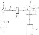
Fig. 1 is the device synoptic diagram according to second aspect present invention;
Fig. 2 is about normalized (002) reflection strength of 200nmInAlAsSb layer on the InAs substrate with 40nmInAs cap rock and the three-dimensional curve diagram of mismatch degree and In percentage;
Fig. 3 is about normalized (004) reflection strength of 200nmInAlAsSb layer on the InAs substrate with 40nmInAs cap rock and the three-dimensional curve diagram of mismatch degree and In percentage;
Fig. 4 is normalized (002) reflection strength of 0.18% mismatch degree intercepting from Fig. 2 and the two-dimensional curve figure of mismatch degree and In percentage;
Fig. 5 (a) is for the ground floor a of the InAsSb twin crystal swing curve figure in (002) reflection;
Fig. 5 (b) is for the second layer b of the InAsSb twin crystal swing curve figure in (002) reflection;
Fig. 6 is normalized (002) reflection strength that intercepts from Fig. 2 and about the curve of Sb percentage;
Fig. 7 is the Sb percentage curve that is calculated about the size of the concentrated window of the relative employing with b of topped ternary layers a of InAsSb; With
Fig. 8 is GaAs or ImAs unit structure cell synoptic diagram.
Embodiment
Device comprises a diffractometer with general assembly shown in Figure 1.Diffractometer can be a Bedescientific D3 high resolving power diffractometer, has a rotary anode source or a Bruker D5000 HR diffractometer that utilizes standard seal pipe x-ray source and the work of Gobel catoptron.Each comprises an x-ray source, and a sample stage 2 and a detecting device 4 that is used to detect from the x ray of sample diffraction are laid a semiconductor material sample 3 of preparing analysis on the sample stage 2.Detecting device is a scintillation detector.X-ray source comprises an electron beam 5 that incides on the copper target 6, and the copper target produces feature x beam 7.Beam passes an optical element 8, and this optical element is to beam 7 monochromatizations and shaping.Optical element is a Si (220) four reflection monochromators (Bruker diffractometer).It selects the part output of K-α feature x ray.The monochromatic x beam that is essentially of gained incides on the sample, and is diffracted at there.The size of sample is in 100 microns~tens millimeters scope.This device provides high photon counting and high source stability, and high-quality data are collected in permission (approximately 2s/ data point) in rational gate time.
By in the scope of about 800 arc microseconds, measuring swing curve, be intensity-angle curve 9 by the swing sample.The data area of allow to collect extending like this to be guaranteeing to comprise all features with remarkable intensity in swing curve, thereby allows the accurate normalization of data.
Quaternary and ternary semiconductor material are as sample.Quaternary and ternary epitaxial deposition are in VGV80H MBE system.This layer is by the thick InAlAsSb of 200nm or InAsSb growth temperature and the 1.1 μ mhr at 450 ℃
-1The InAs substrate of growth rate deposit to 2 inch on form.Because the quaternary sample is a kind of Al of inclusion compound, so the InAs cap rock of 40nm also deposits on the total to prevent the oxidation in air of this layer.The existence of cap rock also makes it possible to the influence of extra play edge thickness is made the assessment of composition measurement stability.
The swing curve that records comprises that several are corresponding to the peak from the diffraction of the incident x ray of each layer of sample and substrate.For the composition of analytic sample, by being to concentrate on the window at center to assess (002) accurate intensity of prohibiting reflection peak at peak with range upon range of mountains.
Utilize the strain regime of (004) reflection layer of estimation sample from the tetragonal crystal system distortion of unit structure cell of symmetry, thereby provide lattice parameter, and utilize asymmetrical (444) reflection to provide the lattice parameter that is parallel to substrate surface perpendicular to substrate surface.This analysis showed that all layer 100% allergic effects, and the estimation of the composition of deriving from the peak position that (004) of match is reflected is not subjected to the influence of stress relaxation.Layer thickness also can be determined by match (004) swing curve.
Utilize business software RADS to carry out the simulation of X ray swing curve according to the TaKagi-Taupin equation.These calculating provide whole dynamic calculation of diffraction energy and consider light beam regulation optics.
For the intensity and the experimental data that can relatively calculate, by under swing curve with general collection in intensity remove each point to each swing curve normalization that records.The error introduced of program can be ignored thus, is detected from the major part of the x ray of (002) planar diffraction guaranteeing as long as collected the interior data of enough big angle of diffraction scope.
The standard method of extracting experiment parameter from x ray swing curve is to utilize the simulation of the experimental data of full dynamic similation and match.Consider simultaneously to calculate, and accurately reproducing theoretically such as " diffraction traction " such phenomenon in the reproduction peak shape, this phenomenon is owing to for example do not comprise the energy spread in source and cause such as the such experiment problem of noise data, and the precision that wafer curvature may serious reflections affect data fitting.In addition, the interference effect that takes place owing to the extra play in the structure such as Pendellosung or thickness edge will cause the problem that peak intensity is brought by specific set of planes in measuring.In the method for carrying out data analysis stable, be to concentrate on the window at center to forbid reflection/diffraction peak intensity at peak for (002) standard of this layer with the peak for these problems.As long as this concentrated window is suitable for making the size of the effective percentage that comprises (002) intensity, but not big to the remarkable result who comprises that other structure is made in the swing curve, the intensity that then records should be not too responsive to accurate peak shape.
Fig. 2 is about normalized (002) reflection strength of 200nmInAlAsSb on the InAs substrate with 40nmInAs cap rock and the three-dimensional curve diagram of mismatch degree and In percentage.Positive according to expectation because very big diffraction difference power between In and the Al can be seen (002) intensity and the strong dependence of III family species.For example, under 0.18% mismatch degree, 20% variation provides the variation of (002) intensity 75% in the In percentage.Have only 6% variation to contrast in this and simulation shown in Figure 3 and normalized (004) intensity.Along the mismatch axle of Fig. 2, the Main Ingredients and Appearance of the variation in (002) reflection strength is come from the diffraction peak scattering strength on every side of substrate.This is regarded as the strong growth of intensity under low mismatch.Come from by the composition along the mismatch axle at the thickness edge due to the InAs that is included in the 40nm in this calculating and also regarded as the slight rising of intensity around 0.4% mismatch degree.It is this because the effect at thickness edge is more obvious in (004) reflection (Fig. 3).In this case, approximately be that the peak displacement of the twice of angle between the substrate peak at (002) peak and the range upon range of mountains value allows to comprise the whole vibrations along the thickness edge of mismatch axle.
Fig. 4 is normalized (002) reflection strength of 0.18% mismatch degree intercepting from Fig. 2 and the two-dimensional curve figure of mismatch degree and In percentage.The concentrated intensity of utilizing the concentrated window of one 50 arcsecond to measure to mark and draw in this curve map for (002) peak of this layer.The composition of this layer of data estimation is In thus
0.873Al
0.127AS
0.855Sb
0.145This value is rationally consistent with composition.By mismatch degree of this layer and the In that calculates from the III family flux that reflection high-energy electron diffraction (RHEED) records
0.86Al
0.14AS
0.85Sb
0.15Vibration before deposition, and suppose a sticking coefficient to III family element.
As previously mentioned, very difficult by the composition of the accurate measurement of other counting quaternary layer.Therefore, in order to obtain to forbid the estimation of the error that produces in (002) Data Matching process of diffraction (002) intensity and calculating, the InAsSb layer of two the complete strains of growing in the standard of experiment.Show respectively among Fig. 5 (a) and 5 (b) for layer a and the twin crystal swing curve of layer b in (002) reflection.Fig. 6 is the curve for 100% layer of (002) reflection strength and Sb percentage that intercepts from Fig. 2.This curve is used to estimate the quaternary layer composition shown in Fig. 5, and relatively these are worth, and utilizes Wei lattice law and reflects the layer mismatch degree that records from their (004) and determine composition.The composition of the InAsSb that the intensity at utilization (002) peak records is respectively InAs for a layer and b layer
99.2Sb
0.8And InAs
97.4Sb
2.6Utilizing the composition of these layers of standard x ray technology calculating is InAs for a layer
99.1Sb
0.9, be InAs for the b layer
97.3Sb
2.7These two technology are 0.1% for two-layer difference.Under the situation of layer a, consider (002) reflection shown in Fig. 5 (a) and substrate peak capable and experienced the relating under extremely low mismatch degree, the unanimity of this degree is more or less astonishing.But, this good certificate of compliance concentration techniques stability that peak shape is changed.
Fig. 7 is about how calculating the curve map of layer a and b and variation with different in width collection window.This figure has proved that again this technology is insensitive to the influence of interfering between the different characteristic in the swing curve.With the maximum deviation of true composition of the layer that from Fig. 6, records be 0.2%.This situation appears in the concentrated window for maximum, comprises the afterbody at (002) peak and thereby comprises the remarkable contribution of other source to intensity.
Fig. 8 is GaAs or ImAs unit structure cell synoptic diagram.Utilization is with correct Bragg angle radiation incident, has a very strong intensity from the diffraction on (004) plane because from the plane 80,81,82,83 and 84 scattering all homophase and: the scattering homophase of Ga atom from the scattering on plane and As atom from the plane.
For the scattering that from label is 82 002 plane, on the structure with 80,82 and 84 scattering homophase from the plane, and atom from the plane 81 and 83 scattering homophase each other, 80,82 and 84 the scattering homophase not from the plane.So the scattering strength at specific direction is ∑ (f
1-f
2)
2, f wherein
1And f
2Be Gallium (f
1) and Arsenic (f
2) scattering power.
In a cubic cell, all atom ∑ (f of same material
1-f
2)=0 is because f
1=f
2Non-vanishing in binary semiconductor alloy such as pure GaAs, but less than the signal ∑ (f from (004) face
1-f
2)
2
But, if f
1' s and/or f
2' among the s some are because replace other alloy atom (as Al replacement Ga, Sb replaces As) with Ga and/or As, then the very little variation by atomic concentration will change ∑ (f significantly
1-f
2)
2, wherein atom has the scattering power that is different from elementary lattice.
Similarly, make and to draw Al/In and/or As/Sb ratio by utilizing scattering angle and scattering strength information in the InAs crystal replacing As with Al substitute I n and/or with Sb, derive the chemical analysis of quaternary alloy.
Such imagination is arranged, in making semiconductor crystal a kind of such machine that is configured to is arranged, check by utilizing the present invention the chemical analysis of crystal checks what is an actual fabrication, what is to wish to make.Therefore know the desired diffraction peak of what measurement of angle (whether be (002), (006), (004) or other), and generally can before rocking test, be positioned at correct position to detecting device and x ray emitter.Can carry out the measurement of diffraction peak position/angle and the intensity under the peak situation then and can produce one measuring composition.Can be at composition scope craft that allows or the composition that utilizes the self-verifying of computing machine to record.In one embodiment, the answer of " qualified " or " defective " is tested and is provided in computer control.Very clear, some are arranged in semiconductor wafer manufacturer process semiconductor wafers is not correct predetermined chemical analysis.If wafer then can continue the making/treatment step of back by the control test.
This system can produce the printing/particular crystal of making or a collection of crystal of absolute concentration.
Need protect the data carrier of executive routine, wherein program is used to control device of the present invention.
Also will understand the present invention and allow to utilize accurate quaternary and ternary semiconductor alloy, the especially chemical analysis of III-V alloy of prohibiting the ionization meter cubic system of angle diffraction at least in one embodiment, thereby determine for example chemical analysis of epitaxial loayer, the accurate angle diffraction of prohibiting for example is (002) or (006) reflection.
The present invention allows to determine the composition of one deck under the situation of any body lattice parameter of not knowing ternary phase.This is useful when can not get high-purity body monocrystalline, under the situation of for example AlAs.
Crystal composition as quaternary compound can be determined by the single x radionetric survey that utilizes peak separation and peak intensity.
This technology allows to carry out composition and judges that the level of alloy is high enough to influence lattice parameter but is not enough to change scattering strength in the ternary alloy three-partalloy that mixes.Can analyze thin buried regions.
Will also be understood that and can in individual event test, judge chemical analysis, needn't be before determining chemical analysis the further feature/parameter of test material.Compare with preceding 8 pairs of crystal swing curves needed in the art, the present invention has saved the considerable time when specimen.
Claims (29)
1. the method for the relative quantity of different chemical element E1 to En in the chemical analysis of a definite crystal semiconductor material, this method comprises from crystalline material diffraction radiation bundle and measures the angle of at least one diffraction peak and the parameter of the intensity of this diffraction radiation of an expression part, this parameter is at least one diffraction peak, or the concentrated area on the part of at least one diffraction peak, at least one is positioned at described angle of diffraction, and by using the radiating scattering power from element E1 to En, the value that the parameter of position and expression intensity derives also utilizes processor to determine the relative quantity of element E1 to En in the chemical analysis of crystalline material.
2. the method for claim 1, wherein the part of diffraction peak or the diffraction energy standard that is in semiconductor material is prohibited angle of diffraction.
3. the method for claim 1, wherein accurate taboo diffraction is the reflection in (002).
4. the method for claim 1, wherein accurate taboo diffraction is the reflection in (006).
5. the method for claim 1, wherein the part of diffraction peak or diffraction energy is the result of (004) reflection.
6. the method for claim 1 comprises that utilization determines the chemical analysis of material to the element that may exist in the understanding of material structure and the material.
7. the method for claim 1, wherein, suppose that crystal semiconductor material includes only the known predetermined chemical element of limited quantity, and processor is in the processing of element scattering power value of the input data that record and storage, wherein only is assumed to be for the scattering power of the known predetermined chemical element of limited quantity to exist.
8. method as claimed in claim 7, wherein, described material comprises four kinds or less chemical element.
9. the method for claim 1 comprises the composition of judging layer of material and utilizes to the understanding of bed thickness or to the hypothesis of the thickness of analyzed layer.
10. the method for claim 1 comprises the composition of judging monolayer material on the material substrate.
11. the method for claim 1 comprises at least two diffraction peaks of measurement or the position of two parts diffraction energy at least, and utilizes the relative quantity of their understanding of position being judged chemical element in the chemical analysis of semiconductor material.
12. the method for claim 1 comprises the diffracted beam intensity of at least two positions of measurement or measures the intensity of two parts diffraction energy at least, and utilizes such understanding to judge the chemical analysis of semiconductor material.
13. the method for claim 1 comprises the intensity of measuring two diffraction peaks or two parts diffraction energy.
14. the method for claim 1, wherein semiconductor material is a kind of quaternary semiconductor material.
15. the method for claim 1, wherein semiconductor material is a kind of ternary semiconductor material.
16. method as claimed in claim 14 also comprises a parameter of the lattice parameter of measuring an expression quaternary semiconductor material, and utilize the intensity of this parameter and diffraction peak or expression intensity parameter, the estimation to material composition is provided in single diffractometry.
17. the method for claim 1, wherein semiconductor material is a kind of III-V semiconductor material.
18. the method for claim 1, wherein analyze to the composition of the semiconductor material of small part generation strain.
19. the method for claim 1, wherein semiconductor material is a kind of monocrystal material.
20. the method for claim 1, wherein with the number percent of every kind of chemical element of being less than or equal to 0.1% error analysis semiconductor material chemical analysis.
21. the method for claim 1 also comprises the parameter of measuring an expression semiconductor material lattice parameter.
22. method as claimed in claim 21, this method are used for the composition of the non-superficial layer that the analyzing semiconductor material buries.
23. the method for claim 1, also comprise the detection composition of comparison semiconductor material with reference to composition, to judge that detected composition equals described with reference to composition or drop on reference near the preset range composition, if and the composition that records is within this scope then produces first output,, the composition that records produces second output if being in outside this scope.
24. chemical analysis analytical equipment, comprise a sample retainer, an energy-beam source, one or more detecting devices, a controller and a processor, described controller is used for the control energy electron gun, described detecting device is used for the guiding energy bundle and comes the diffraction energy that also detects on the sample that is fixed on sample retainer at the angle of diffraction place, described detecting device and processor coupling, processor is used with the signal of the concentrated intensity of representing diffraction peak position and a part of diffraction peak, and processor is arranged so that in use it uses detection signal, in conjunction with the hypothesis that has which kind of predetermined-element in the sample, and the scattering power of atom in the element of having supposed to have, or depend on the factor of the scattering power of predetermined-element, with the relative quantity of chemical element predetermined in the chemical analysis of estimation sample.
25. device as claimed in claim 24, wherein having one is used for making the user to be selected input unit by the element of the chemical element of hypothesis existence to the sample that processor identification will be analyzed, therefore, the chemical element scattering power or the factor that depends on scattering power are used for determining the relative quantity of sample chemical element by processor, processor is applicable to according to input variable that records from described detecting device and the plain scattering power of a sub-component in the use, or, operate with its processor by the child group that this element of operation selects input unit to select from bigger group of derivation value that stores the selection of element scattering power.
26. device as claimed in claim 24, wherein sample retainer, energy-beam source and described detecting device are preset in the precalculated position, this precalculated position is relevant by so a kind of relation each other, and promptly the sample for known type disposes at least one detecting device, detects so that prohibit angle of diffraction in standard.
27. method of making semiconductor wafer, comprise and make a semiconductor wafer, the composition of methods analyst wafer according to claim 1 with test whether by or can't pass the analysis of components test, if and wafer has the composition in the preset parameter, then wafer is carried out prefabricated operation to make wafer, if wafer has the composition beyond the preset parameter scope, then discharge wafer further handling or to make operation, the wafer of discharge at least without undergoing they passed through can a receptible treatment step.
28. method as claimed in claim 27, wherein, the wafer by analysis of components test and/or the wafer of wafer manufacturing thus be subsidiary to be had and confirms that they are by test or provide the data of the details of their analysis of components.
29. the method for the relative quantity of different chemical element in the chemical analysis of a definite crystal quaternary semiconductor material, this method comprises from crystalline material diffraction radiation bundle and measures the angle of a diffraction peak at least and in the concentrated intensity of the diffraction radiation of at least a portion of this angle of diffraction, and puts the value that the concentrated intensity with the diffraction radiation of described at least a portion causes from the radiating scattering power and bit of element and utilize processor to determine the relative quantity of element the chemical analysis of crystalline material by using.
Applications Claiming Priority (4)
| Application Number | Priority Date | Filing Date | Title |
|---|---|---|---|
| GBGB9905953.7A GB9905953D0 (en) | 1999-03-16 | 1999-03-16 | Method and apparatus for the analysis of material composition |
| GB9905953.7 | 1999-03-16 | ||
| GB0000392.1 | 2000-01-11 | ||
| GB0000392A GB0000392D0 (en) | 2000-01-11 | 2000-01-11 | Method and apparatus for the analysis of material composition |
Publications (2)
| Publication Number | Publication Date |
|---|---|
| CN1354832A CN1354832A (en) | 2002-06-19 |
| CN1187604C true CN1187604C (en) | 2005-02-02 |
Family
ID=26243357
Family Applications (1)
| Application Number | Title | Priority Date | Filing Date |
|---|---|---|---|
| CNB008076669A Expired - Fee Related CN1187604C (en) | 1999-03-16 | 2000-03-15 | Method and apparatus for analysis of material composition |
Country Status (7)
| Country | Link |
|---|---|
| US (1) | US6907107B1 (en) |
| EP (1) | EP1163507A2 (en) |
| JP (1) | JP2003532862A (en) |
| KR (1) | KR20020011369A (en) |
| CN (1) | CN1187604C (en) |
| AU (1) | AU3180800A (en) |
| WO (1) | WO2000055608A2 (en) |
Families Citing this family (13)
| Publication number | Priority date | Publication date | Assignee | Title |
|---|---|---|---|---|
| EP1463971A2 (en) * | 2001-12-12 | 2004-10-06 | The Regents of the University of California | INTEGRATED CRYSTAL MOUNTING AND ALIGNMENT SYSTEM FOR HIGH−THROUGHPUT BIOLOGICAL CRYSTALLOGRAPHY |
| JP3889388B2 (en) * | 2003-10-06 | 2007-03-07 | 株式会社リガク | Membrane structure analysis method and apparatus |
| US7579616B2 (en) * | 2007-04-10 | 2009-08-25 | International Business Machines Corporation | Four-terminal programmable via-containing structure and method of fabricating same |
| US7561269B2 (en) * | 2007-12-14 | 2009-07-14 | Tokyo Electron Limited | Optical measurement system with systematic error correction |
| US8605858B2 (en) | 2011-06-27 | 2013-12-10 | Honeywell International Inc. | Methods and systems for inspecting structures for crystallographic imperfections |
| US9835570B2 (en) * | 2013-09-13 | 2017-12-05 | The United States Of America As Represented By The Administrator Of Nasa | X-ray diffraction (XRD) characterization methods for sigma=3 twin defects in cubic semiconductor (100) wafers |
| US9829448B2 (en) * | 2014-10-30 | 2017-11-28 | Bruker Jv Israel Ltd. | Measurement of small features using XRF |
| AU2017328259B2 (en) * | 2016-09-19 | 2021-11-04 | Security Matters Ltd. | X-ray fluorescence system and method for identifying samples |
| CN110767562B (en) * | 2019-09-23 | 2021-11-16 | 长江存储科技有限责任公司 | Method for measuring content of film phase |
| US11341629B2 (en) | 2020-07-02 | 2022-05-24 | Pratt & Whitney Canada Corp. | Systems and methods for generating an inspection image of an object from radiographic imaging |
| US20220198326A1 (en) * | 2020-12-17 | 2022-06-23 | Virtual Control Limited | Spectral data processing for chemical analysis |
| CN113984852B (en) * | 2021-09-27 | 2023-07-07 | 泉州师范学院 | Heterojunction material construction and characterization method based on first sex principle calculation |
| CN118156358B (en) * | 2024-05-11 | 2024-08-09 | 山东大学 | SiC semiconductor detector, ore component analysis apparatus and method |
Family Cites Families (15)
| Publication number | Priority date | Publication date | Assignee | Title |
|---|---|---|---|---|
| DE2637945C3 (en) | 1976-08-23 | 1979-02-08 | Siemens Ag, 1000 Berlin Und 8000 Muenchen | ROENTHEN POWDER DIFFACTOMETER |
| DE3439471A1 (en) | 1984-10-27 | 1986-04-30 | MTU Motoren- und Turbinen-Union München GmbH, 8000 München | METHOD AND DEVICE FOR TESTING SINGLE-CRYSTAL OBJECTS |
| US4575922A (en) | 1984-11-05 | 1986-03-18 | Burroughs Corporation | Method of fabricating integrated circuits incorporating steps to detect presence of gettering sites |
| EP0186924A3 (en) | 1984-12-31 | 1988-10-19 | Koninklijke Philips Electronics N.V. | Polycrystalline x-ray spectrometer |
| GB2169480B (en) | 1985-01-03 | 1988-12-07 | Erno Raumfahrttechnik Gmbh | A method of non-destructive testing of structural members |
| DD270770A1 (en) * | 1988-04-18 | 1989-08-09 | Freiberg Bergakademie | ROENTGENDIFRACTOMETRIC STUDY FOR THE SITE-RELATED SIMULTANEOUS DETECTION OF VARIATIONS OF THE STOECHOMETRY STATE AND MICRODEFEKTHAUSHALTES IN SINGLE CRYSTALLINE COMPOSITION STRUCTURES |
| US5007072A (en) | 1988-08-03 | 1991-04-09 | Ion Track Instruments | X-ray diffraction inspection system |
| US4928294A (en) | 1989-03-24 | 1990-05-22 | U.S. Government As Represented By The Director, National Security Agency | Method and apparatus for line-modified asymmetric crystal topography |
| US5148458A (en) * | 1990-01-18 | 1992-09-15 | Clayton Ruud | Method and apparatus for simultaneous phase composition and residual stress measurement by x-ray diffraction |
| FR2692700A1 (en) * | 1992-06-17 | 1993-12-24 | Philips Electronique Lab | A measurement signal processing device corresponding to the X-ray intensity reflected by a multilayer structure on a substrate. |
| US5414747A (en) * | 1993-02-22 | 1995-05-09 | The Penn State Research Foundation | Method and apparatus for in-process analysis of polycrystalline films and coatings by x-ray diffraction |
| GB2289833B (en) | 1994-05-24 | 1998-04-22 | Mitsubishi Electric Corp | Method and apparatus for evaluating thin-film multilayer structure |
| DE19510168C2 (en) | 1995-03-21 | 2001-09-13 | Heimann Systems Gmbh & Co | Method and device for determining crystalline and polycrystalline materials in an examination area |
| GB9519687D0 (en) | 1995-09-27 | 1995-11-29 | Schlumberger Ltd | Method of determining earth formation characteristics |
| US6577705B1 (en) * | 2001-04-02 | 2003-06-10 | William Chang | Combinatorial material analysis using X-ray capillary optics |
-
2000
- 2000-03-15 WO PCT/GB2000/000951 patent/WO2000055608A2/en active IP Right Grant
- 2000-03-15 CN CNB008076669A patent/CN1187604C/en not_active Expired - Fee Related
- 2000-03-15 US US09/936,560 patent/US6907107B1/en not_active Expired - Fee Related
- 2000-03-15 JP JP2000605190A patent/JP2003532862A/en not_active Withdrawn
- 2000-03-15 EP EP00909525A patent/EP1163507A2/en not_active Ceased
- 2000-03-15 AU AU31808/00A patent/AU3180800A/en not_active Abandoned
- 2000-03-15 KR KR1020017011758A patent/KR20020011369A/en active IP Right Grant
Also Published As
| Publication number | Publication date |
|---|---|
| EP1163507A2 (en) | 2001-12-19 |
| WO2000055608A3 (en) | 2001-02-08 |
| US6907107B1 (en) | 2005-06-14 |
| JP2003532862A (en) | 2003-11-05 |
| AU3180800A (en) | 2000-10-04 |
| CN1354832A (en) | 2002-06-19 |
| KR20020011369A (en) | 2002-02-08 |
| WO2000055608A2 (en) | 2000-09-21 |
Similar Documents
| Publication | Publication Date | Title |
|---|---|---|
| CN1187604C (en) | Method and apparatus for analysis of material composition | |
| Dolabella et al. | Lattice strain and defects analysis in nanostructured semiconductor materials and devices by high‐resolution X‐ray diffraction: Theoretical and practical aspects | |
| Mandal et al. | Advances in high-resolution radiation detection using 4H-SiC epitaxial layer devices | |
| Lorenz et al. | Anomalous ion channeling in AlInN/GaN bilayers: determination of the strain state | |
| Hart | Bragg angle measurement and mapping | |
| US7885383B1 (en) | Method for measuring crystallite size with a two-dimensional X-ray diffractometer | |
| CN102879411A (en) | Method for testing crystal by X-ray diffraction | |
| Fewster | A new theory for X-ray diffraction | |
| Tran et al. | Measurement of the x-ray mass attenuation coefficient and the imaginary part of the form factor of silicon using synchrotron radiation | |
| Ziska et al. | Quantifying the elemental distribution in solar cells from X-ray fluorescence measurements with multiple detector modules | |
| Prabket et al. | Resistivity profile of epitaxial layer for the new ALICE ITS sensor | |
| US9880115B2 (en) | Method for characterizing a material | |
| JP6904313B2 (en) | Method for evaluating carbon concentration in silicon single crystal | |
| Butcher et al. | Drift time variations in CdZnTe detectors measured with alpha particles and gamma rays: Their correlation with detector response | |
| Stieghorst et al. | Determination of boron and hydrogen in materials for multicrystalline solar cell production with prompt gamma activation analysis | |
| Johns | Materials development for nuclear security: Bismuth triiodide room temperature semiconductor detectors | |
| Tolkiehn et al. | Kinematical x-ray standing waves for crystal structure investigations | |
| US12099025B2 (en) | Device and method for measuring short-wavelength characteristic X-ray diffraction based on array detection | |
| US20220412901A1 (en) | Device and method for measuring short-wavelength characteristic x-ray diffraction based on array detection | |
| Yoshida et al. | Mössbauer spectroscopic microscope study on diffusion and segregation of Fe impurities in mc-Si wafer | |
| Xiao et al. | Preliminary experiment for residual stress analysis at the advanced photon source | |
| James et al. | Effect of HgI2 crystal nonuniformities on gamma-ray response | |
| Penkova | Defect characterization in 4% cadmium zinc telluride semiconductors | |
| Abou-Ras et al. | Electron backscatter diffraction: Exploring the microstructure in Cu (In, Ga)(S, Se) 2 and CdTe thin-film solar cells | |
| Pietsch | White beam Laue diffraction of polycrystalline materials using 3D energy dispersive detector (pnCCD) |
Legal Events
| Date | Code | Title | Description |
|---|---|---|---|
| C10 | Entry into substantive examination | ||
| SE01 | Entry into force of request for substantive examination | ||
| C06 | Publication | ||
| PB01 | Publication | ||
| C14 | Grant of patent or utility model | ||
| GR01 | Patent grant | ||
| C17 | Cessation of patent right | ||
| CF01 | Termination of patent right due to non-payment of annual fee |
Granted publication date: 20050202 Termination date: 20100315 |