Multilayer frequency band separator with parasitic earthing capacitance
Invention field
The present invention relates to a kind of filter element (filtering device usedin wireless communication) that is used for radio communication, relate in particular to a kind of multilayer frequency band separator (multilayer band separator), it uses transmission line to work as inductance, and utilize parasitic earthing capacitance to shorten the ground connection length of transmission line to reach the downsizing purpose, this has near high pass filter characteristic, and therefore less insertion loss is arranged.
Background technology
In radio communication (wireless communication), multi-band operation has been inevasible mode.In present wireless communication system, (be duplexer (duplexer) or band separator (band separator), generally speaking the principal element of Kao Lving has (1) to insert loss (insertion loss) to design a double frequency filter; (2) protection bandwidth (guard band); (3) insulativity (isolation); (4) outer (outband) inhibition degree (rejection) of band.Very wide when buffer zone, when requiring preferable insertion loss and insulativity again, utilize low pass filter (lowpass filter) more suitable with the combination of high pass filter (highpass filter).Very wide when buffer zone, require preferable insertion loss again and when not minding insulativity and frequency range thereof, utilize the combination of two band stop filters (bandstop filter) comparatively suitable.Require size when focusing on, when outer inhibitions of band spent, utilize that two band pass filters (bandpass filter) or a band are logical to be added one and be with the combination that hinders comparatively suitable.Very narrow and when requiring preferable insertion loss when buffer zone, utilize band stop filter (bandstop filter) comparatively suitable with the combination of high pass filter (highpass filter).For example, in the double frequency filter application of Taiwan GSM900 and DCS1800 or in the double frequency filter of U.S. MPS900 and PCS1900 is used, buffer zone is very wide, and require than low insertion loss, therefore be fit to adopt the combination of low pass filter and high pass filter or utilize the combination of two band stop filters comparatively suitable.
Fig. 1 one is used for the multiple field frequency separation device (multilayered frequency separator) of GSM/DCS dual-band mobile phone by two band stop filters combinations traditionally.In Fig. 1, two bandreject filtering Notch 1, Notch 2 comprise that respectively a capacitor makes up with (shunt) in parallel of an inductor.As shown in Figure 1, when signal T1 imports, because the difference of LC parameter value, and make this filter respectively at frequency f 1=900MHz output signal T3 and at frequency f 2=1800 or 1900MHz output signal T2, the double frequency output signal of its output is shown among Fig. 2.Because the GSM/DCS dual-band mobile phone is to account for more than 10% of whole frequency range for insulation width (isolation bandwidth) in the standard that requires of 20dB, therefore, this class circuit often can't satisfy the requirement of GSM/DCS dual-band mobile phone to insulation width.In view of the above, with reference to figure 3, in the U.S. Patent number 5,880,649 that Tai et al. is provided, provide one to improve circuit.In Fig. 3, except that comprising two band stop filters, still comprise low pass filter and the LC high pass filter that constitutes in parallel that a capacitor constitutes.As shown in Figure 3, when signal T11 respectively through two band stop filter Notch 3, Notch 4, reach corresponding low pass filter and high pass filter and produce output signal T22 at frequency f 1=900MHz generation output signal T33 and at frequency f 2=1800 or 1900MHz respectively, the double frequency output signal of its output is shown among Fig. 4.As shown in Figure 4, this circuit layout can make the frequency range at 20dB place strengthen with the compliance with system requirement, but must increase the comparatively complicated of one-level filter so that circuit change, thereby further increases manufacturing cost.
Summary of the invention
In view of this, a purpose of the present invention provides a multilayer frequency band separator with parasitic earthing capacitance, it uses the ground connection transmission line to work as inductance, and utilize parasitic earthing capacitance to shorten the ground connection length of transmission line to reach the purpose of downsizing, and because of its characteristic near high pass filter, so less insertion loss is arranged.
Another object of the present invention provide one its multilayer frequency band separator of parasitic earthing capacitance is arranged, its attenuation pole with low pass filter (attenuate pole) changes into open circuit limit (open-circuit pole), and produce with low pass filter and to be connected in series effect and to produce an attenuation pole with the low frequency part at front end, so need not increase filter order and can obtain higher inhibition effect.
The invention provides a multilayer frequency band separator with parasitic earthing capacitance, make the present invention have less insertion loss and higher inhibition effect because of using parasitic capacitance and transmission line.This multilayer frequency band separator with parasitic earthing capacitance comprises high pass filter (quasi-highpassfilter), half lump type low pass filter (semi-lumped lowpass filter) and a phase shift device (phase shifter) surely.This accurate high pass filter comprises that the 3rd capacitor, an one end that connects input signal connects the 3rd capacitor and the 4th capacitor of other end ground connection, an one end ground connection and the other end connect that the inductive element of the 3rd capacitor and the 4th capacitor interface point and an one end connect the 3rd, the 4th capacitor and this inductive element interface point and the other end connects one second output to produce second capacitor of a high frequency output signal.This phase shift device is one to be connected to the input signals kind of thread elements.This half lump type low pass filter comprises that an one end connects that this phase-shifts device does not connect an end of input signal and the other end connects one first output is connected across first capacitor on this resistance element with the resistance element and that produces a low frequency output signal.
Above-mentioned this inductive element and this resistance element are to dispose in transmission line (transmission line) mode, make the present invention show the characteristic of approximate (quasi) high pass filter thereby have less insertion loss.Simultaneously, this phase shift device also disposes in transmission line (transmission line) mode, make the present invention the attenuation pole of this half lump type low pass filter can be changed into the open circuit limit, and both serial connections can produce an attenuation pole in the low frequency part of front end, so can obtain higher inhibition effect and increase insulation width (isolation bandwidth) under the situation that does not increase filter order.
Description of drawings
For allow above-mentioned and other purpose of the present invention, feature, can be more apparent with advantage, preferred embodiment cited below particularly, and cooperate appended graphicly is described in detail below:
Fig. 1 is a traditional multilayer frequency band separator;
Fig. 2 is characteristic curve (characteristics) figure of the circuit response (Circuit response) of Fig. 1;
Fig. 3 is another traditional multilayer frequency band separator;
Fig. 4 is characteristic curve (characteristics) figure of the circuit response (Circuit response) of Fig. 3;
Fig. 5 be the present invention its have the multilayer frequency band separator of parasitic earthing capacitance;
Fig. 6 is characteristic curve (characteristics) figure of the circuit response (Circuit response) of Fig. 5; And
Fig. 7 a-7h figure is the circuit layout schematic diagram of Fig. 5;
Fig. 8 is the insertion loss schematic diagram of Fig. 5 circuit;
Fig. 9 is the linear frequency response curve of the present invention with capacitor C 11.
Embodiment
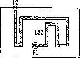
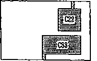
With reference to figure 5, be the multilayer frequency band separator that the present invention has parasitic earthing capacitance.For the purpose of explanation, be example with some band separators, yet this example is only in order to explanation but not in order to restriction.In Fig. 5, this multilayer frequency band separator with parasitic earthing capacitance comprises high pass filter (quasi-highpass filter) QHF, half lump type low pass filter (semi-lumpedlowpass filter) SLF and a phase shift device (phase shifter) L11 surely.As shown in Figure 5, this accurate high pass filter comprises that the 3rd capacitor C33, an one end that connects input signal Ant connects the 3rd capacitor C33 and the 4th capacitor C44 of other end ground connection, an one end ground connection and the other end connect that the inductive element L33 of the 3rd capacitor C33 and the 4th capacitor C44 interface point P3 and an one end connect the 3rd, the 4th capacitor C33, C44 and this inductive element L33 interface point P3 and the other end connects one second output DCS to produce the second capacitor C22 of a high frequency output signal.This phase shift device L11 one is connected to the input signals kind of thread elements.This half lump type low pass filter SLF comprises that an one end connects that this phase-shifts device L11 does not connect an end P1 of input signal and the other end connects one first output GSM is connected across the first capacitor C11 on this resistance element L22 with the resistance element L22 and that produces a low frequency output signal.
This accurate high pass filter uses the ground connection transmission line as inductive element L33, and utilize parasitic earthing capacitance C44 to shorten the ground connection length of transmission line to reach the downsizing purpose, because the reponse charactersitic of circuit near high pass filter, therefore has less insertion loss (low insertion loss) (see figure 8).This phase shift device L11 changes into open circuit limit (Fig. 8) with the attenuation pole (attenuationpole) of this half lump type low pass filter SLF at input Ant, and produce with this half lump type low pass filter SLF and to be connected in series effect, produce an attenuation pole so as to low frequency part, make the present invention must not increase any filter order and can obtain higher inhibition effect and increase insulation width (isolation bandwidth) at the high frequency response curve.This half lump type low pass filter SLF, the insertion loss when low frequency is operated | the insertion loss when S11| and high-frequency operation | S21| is that linear frequency response wc with capacitor C 11 becomes (see figure 9) in the present invention, to obtain optimal inhibition degree as shown in Figure 6.
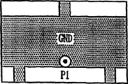
Fig. 7 a-7h is configuration (layout) schematic diagram of Fig. 5.Shown in Fig. 7 a, layout C11 and L11 also reserve through hole (via) to be connected in series each layer use at stain sign place, and this through hole also is the contact P1 among Fig. 5.Shown in Fig. 7 b, only layout C11 produces required removal capacitor (discrete capacitor) to cooperate with above-mentioned C11.Shown in Fig. 7 c, layout one protective ground layer in order to isolating the L22 of layout in Fig. 7 d subsequently, and produces effect in parallel with C11.Similarly, in Fig. 7 e, also use a protective ground layer, in order to isolating the C22 of layout, C33 in Fig. 7 f subsequently, and produce effect in parallel with it, wherein, must keep a suitable distance between C22, the C33.Shown in Fig. 7 g, layout L 33, C22 and C33 to form parallel circuits, wherein, do not have spacing between C22 and C33, so and the C22 among Fig. 7 f and C33 effect can produce parasitic capacitance C44 shown in Fig. 7 g.At last, with each signal I/O, comprise input signal Ant end, high frequency output DCS, low frequency output GSM and earth terminal GND, layout becomes the position shown in Fig. 7 h, just so finish the configuration of circuit among Fig. 5.
Though the present invention with some preferred embodiment narrations as above; right its is not in order to limit the present invention; any personage who knows this technology; in without departing from the spirit or scope of the invention; change and retouching when doing, so protection scope of the present invention is as the criterion when looking the protection range that claim defines.