CN116387027A - Multilayer electronic component - Google Patents
Multilayer electronic component Download PDFInfo
- Publication number
- CN116387027A CN116387027A CN202211658860.5A CN202211658860A CN116387027A CN 116387027 A CN116387027 A CN 116387027A CN 202211658860 A CN202211658860 A CN 202211658860A CN 116387027 A CN116387027 A CN 116387027A
- Authority
- CN
- China
- Prior art keywords
- multilayer electronic
- electronic assembly
- electrode
- insulating layer
- disposed
- Prior art date
- Legal status (The legal status is an assumption and is not a legal conclusion. Google has not performed a legal analysis and makes no representation as to the accuracy of the status listed.)
- Pending
Links
- 238000007747 plating Methods 0.000 claims abstract description 308
- XUIMIQQOPSSXEZ-UHFFFAOYSA-N Silicon Chemical compound [Si] XUIMIQQOPSSXEZ-UHFFFAOYSA-N 0.000 claims abstract description 25
- 229910052710 silicon Inorganic materials 0.000 claims abstract description 25
- 239000010703 silicon Substances 0.000 claims abstract description 25
- 239000010410 layer Substances 0.000 claims description 755
- 229910052751 metal Inorganic materials 0.000 claims description 53
- 239000002184 metal Substances 0.000 claims description 53
- ZOXJGFHDIHLPTG-UHFFFAOYSA-N Boron Chemical compound [B] ZOXJGFHDIHLPTG-UHFFFAOYSA-N 0.000 claims description 46
- 229910052796 boron Inorganic materials 0.000 claims description 46
- PXHVJJICTQNCMI-UHFFFAOYSA-N nickel Substances [Ni] PXHVJJICTQNCMI-UHFFFAOYSA-N 0.000 claims description 32
- 239000011521 glass Substances 0.000 claims description 28
- VYPSYNLAJGMNEJ-UHFFFAOYSA-N Silicium dioxide Chemical group O=[Si]=O VYPSYNLAJGMNEJ-UHFFFAOYSA-N 0.000 claims description 16
- 229910052788 barium Inorganic materials 0.000 claims description 16
- DSAJWYNOEDNPEQ-UHFFFAOYSA-N barium atom Chemical compound [Ba] DSAJWYNOEDNPEQ-UHFFFAOYSA-N 0.000 claims description 16
- ZFZQOKHLXAVJIF-UHFFFAOYSA-N zinc;boric acid;dihydroxy(dioxido)silane Chemical compound [Zn+2].OB(O)O.O[Si](O)([O-])[O-] ZFZQOKHLXAVJIF-UHFFFAOYSA-N 0.000 claims description 14
- 239000010949 copper Substances 0.000 claims description 13
- 229910045601 alloy Inorganic materials 0.000 claims description 10
- 239000000956 alloy Substances 0.000 claims description 10
- 229910052802 copper Inorganic materials 0.000 claims description 9
- 229910000990 Ni alloy Inorganic materials 0.000 claims description 8
- 239000012790 adhesive layer Substances 0.000 claims description 8
- 239000000377 silicon dioxide Substances 0.000 claims description 8
- 235000012239 silicon dioxide Nutrition 0.000 claims description 8
- 229910052759 nickel Inorganic materials 0.000 claims description 5
- RYGMFSIKBFXOCR-UHFFFAOYSA-N Copper Chemical compound [Cu] RYGMFSIKBFXOCR-UHFFFAOYSA-N 0.000 claims description 4
- 238000000034 method Methods 0.000 description 38
- 239000000463 material Substances 0.000 description 34
- 230000035515 penetration Effects 0.000 description 25
- 230000008569 process Effects 0.000 description 17
- 230000032798 delamination Effects 0.000 description 16
- 229910000679 solder Inorganic materials 0.000 description 13
- 239000000758 substrate Substances 0.000 description 13
- 238000010586 diagram Methods 0.000 description 12
- 230000005855 radiation Effects 0.000 description 12
- 239000000919 ceramic Substances 0.000 description 11
- 239000003985 ceramic capacitor Substances 0.000 description 11
- 230000000694 effects Effects 0.000 description 11
- 238000010304 firing Methods 0.000 description 10
- 239000011347 resin Substances 0.000 description 10
- 229920005989 resin Polymers 0.000 description 10
- 238000005259 measurement Methods 0.000 description 8
- 239000007769 metal material Substances 0.000 description 8
- QVGXLLKOCUKJST-UHFFFAOYSA-N atomic oxygen Chemical compound [O] QVGXLLKOCUKJST-UHFFFAOYSA-N 0.000 description 7
- QVQLCTNNEUAWMS-UHFFFAOYSA-N barium oxide Chemical compound [Ba]=O QVQLCTNNEUAWMS-UHFFFAOYSA-N 0.000 description 7
- 238000005520 cutting process Methods 0.000 description 7
- 239000001301 oxygen Substances 0.000 description 7
- 229910052760 oxygen Inorganic materials 0.000 description 7
- 239000010936 titanium Substances 0.000 description 7
- KDLHZDBZIXYQEI-UHFFFAOYSA-N Palladium Chemical compound [Pd] KDLHZDBZIXYQEI-UHFFFAOYSA-N 0.000 description 6
- BASFCYQUMIYNBI-UHFFFAOYSA-N platinum Chemical compound [Pt] BASFCYQUMIYNBI-UHFFFAOYSA-N 0.000 description 6
- 239000000843 powder Substances 0.000 description 6
- 230000035939 shock Effects 0.000 description 6
- 239000011575 calcium Substances 0.000 description 5
- 239000012535 impurity Substances 0.000 description 5
- 239000012466 permeate Substances 0.000 description 5
- 229910004298 SiO 2 Inorganic materials 0.000 description 4
- 238000000231 atomic layer deposition Methods 0.000 description 4
- 238000005229 chemical vapour deposition Methods 0.000 description 4
- 230000007797 corrosion Effects 0.000 description 4
- 238000005260 corrosion Methods 0.000 description 4
- 238000005336 cracking Methods 0.000 description 4
- 238000009792 diffusion process Methods 0.000 description 4
- 238000007598 dipping method Methods 0.000 description 4
- 230000003628 erosive effect Effects 0.000 description 4
- 239000010931 gold Substances 0.000 description 4
- 238000003475 lamination Methods 0.000 description 4
- 230000000149 penetrating effect Effects 0.000 description 4
- 230000009467 reduction Effects 0.000 description 4
- 238000007789 sealing Methods 0.000 description 4
- 239000000654 additive Substances 0.000 description 3
- 230000002776 aggregation Effects 0.000 description 3
- 238000004220 aggregation Methods 0.000 description 3
- JRPBQTZRNDNNOP-UHFFFAOYSA-N barium titanate Chemical compound [Ba+2].[Ba+2].[O-][Ti]([O-])([O-])[O-] JRPBQTZRNDNNOP-UHFFFAOYSA-N 0.000 description 3
- 229910002113 barium titanate Inorganic materials 0.000 description 3
- 230000008878 coupling Effects 0.000 description 3
- 238000010168 coupling process Methods 0.000 description 3
- 238000005859 coupling reaction Methods 0.000 description 3
- 230000007547 defect Effects 0.000 description 3
- 230000005496 eutectics Effects 0.000 description 3
- 150000002739 metals Chemical class 0.000 description 3
- 239000000203 mixture Substances 0.000 description 3
- 239000002994 raw material Substances 0.000 description 3
- 229910018072 Al 2 O 3 Inorganic materials 0.000 description 2
- 239000004593 Epoxy Substances 0.000 description 2
- 239000001856 Ethyl cellulose Substances 0.000 description 2
- ZZSNKZQZMQGXPY-UHFFFAOYSA-N Ethyl cellulose Chemical compound CCOCC1OC(OC)C(OCC)C(OCC)C1OC1C(O)C(O)C(OC)C(CO)O1 ZZSNKZQZMQGXPY-UHFFFAOYSA-N 0.000 description 2
- BQCADISMDOOEFD-UHFFFAOYSA-N Silver Chemical compound [Ag] BQCADISMDOOEFD-UHFFFAOYSA-N 0.000 description 2
- ATJFFYVFTNAWJD-UHFFFAOYSA-N Tin Chemical compound [Sn] ATJFFYVFTNAWJD-UHFFFAOYSA-N 0.000 description 2
- RTAQQCXQSZGOHL-UHFFFAOYSA-N Titanium Chemical compound [Ti] RTAQQCXQSZGOHL-UHFFFAOYSA-N 0.000 description 2
- 239000002253 acid Substances 0.000 description 2
- NIXOWILDQLNWCW-UHFFFAOYSA-N acrylic acid group Chemical group C(C=C)(=O)O NIXOWILDQLNWCW-UHFFFAOYSA-N 0.000 description 2
- 239000003513 alkali Substances 0.000 description 2
- 238000013459 approach Methods 0.000 description 2
- 239000003990 capacitor Substances 0.000 description 2
- 229910010293 ceramic material Inorganic materials 0.000 description 2
- 230000007423 decrease Effects 0.000 description 2
- 235000019325 ethyl cellulose Nutrition 0.000 description 2
- 229920001249 ethyl cellulose Polymers 0.000 description 2
- PCHJSUWPFVWCPO-UHFFFAOYSA-N gold Chemical compound [Au] PCHJSUWPFVWCPO-UHFFFAOYSA-N 0.000 description 2
- 229910052737 gold Inorganic materials 0.000 description 2
- 239000011810 insulating material Substances 0.000 description 2
- 238000004519 manufacturing process Methods 0.000 description 2
- 229910052763 palladium Inorganic materials 0.000 description 2
- 229910052697 platinum Inorganic materials 0.000 description 2
- 239000002952 polymeric resin Substances 0.000 description 2
- 238000007639 printing Methods 0.000 description 2
- 239000000047 product Substances 0.000 description 2
- 238000000926 separation method Methods 0.000 description 2
- 229910052709 silver Inorganic materials 0.000 description 2
- 239000004332 silver Substances 0.000 description 2
- 238000003980 solgel method Methods 0.000 description 2
- 239000000126 substance Substances 0.000 description 2
- 229920003002 synthetic resin Polymers 0.000 description 2
- 229910052719 titanium Inorganic materials 0.000 description 2
- WFKWXMTUELFFGS-UHFFFAOYSA-N tungsten Chemical compound [W] WFKWXMTUELFFGS-UHFFFAOYSA-N 0.000 description 2
- 229910052721 tungsten Inorganic materials 0.000 description 2
- 239000010937 tungsten Substances 0.000 description 2
- 239000004925 Acrylic resin Substances 0.000 description 1
- 229920000178 Acrylic resin Polymers 0.000 description 1
- OYPRJOBELJOOCE-UHFFFAOYSA-N Calcium Chemical compound [Ca] OYPRJOBELJOOCE-UHFFFAOYSA-N 0.000 description 1
- 229910010413 TiO 2 Inorganic materials 0.000 description 1
- HCHKCACWOHOZIP-UHFFFAOYSA-N Zinc Chemical compound [Zn] HCHKCACWOHOZIP-UHFFFAOYSA-N 0.000 description 1
- QCWXUUIWCKQGHC-UHFFFAOYSA-N Zirconium Chemical compound [Zr] QCWXUUIWCKQGHC-UHFFFAOYSA-N 0.000 description 1
- 230000000996 additive effect Effects 0.000 description 1
- 239000000853 adhesive Substances 0.000 description 1
- 230000001070 adhesive effect Effects 0.000 description 1
- PNEYBMLMFCGWSK-UHFFFAOYSA-N aluminium oxide Inorganic materials [O-2].[O-2].[O-2].[Al+3].[Al+3] PNEYBMLMFCGWSK-UHFFFAOYSA-N 0.000 description 1
- 239000011230 binding agent Substances 0.000 description 1
- 230000015572 biosynthetic process Effects 0.000 description 1
- 229910052791 calcium Inorganic materials 0.000 description 1
- 238000005253 cladding Methods 0.000 description 1
- 239000002131 composite material Substances 0.000 description 1
- 150000001875 compounds Chemical class 0.000 description 1
- 230000003247 decreasing effect Effects 0.000 description 1
- 239000002270 dispersing agent Substances 0.000 description 1
- 239000003822 epoxy resin Substances 0.000 description 1
- 239000007789 gas Substances 0.000 description 1
- 238000007646 gravure printing Methods 0.000 description 1
- LNEPOXFFQSENCJ-UHFFFAOYSA-N haloperidol Chemical compound C1CC(O)(C=2C=CC(Cl)=CC=2)CCN1CCCC(=O)C1=CC=C(F)C=C1 LNEPOXFFQSENCJ-UHFFFAOYSA-N 0.000 description 1
- 238000003384 imaging method Methods 0.000 description 1
- 230000006872 improvement Effects 0.000 description 1
- 229910010272 inorganic material Inorganic materials 0.000 description 1
- 239000011147 inorganic material Substances 0.000 description 1
- 238000009434 installation Methods 0.000 description 1
- 230000010354 integration Effects 0.000 description 1
- 239000007788 liquid Substances 0.000 description 1
- 239000004973 liquid crystal related substance Substances 0.000 description 1
- 230000004048 modification Effects 0.000 description 1
- 238000012986 modification Methods 0.000 description 1
- 230000003287 optical effect Effects 0.000 description 1
- 239000011368 organic material Substances 0.000 description 1
- 239000003960 organic solvent Substances 0.000 description 1
- 230000035699 permeability Effects 0.000 description 1
- 229920000647 polyepoxide Polymers 0.000 description 1
- 238000007650 screen-printing Methods 0.000 description 1
- 230000000087 stabilizing effect Effects 0.000 description 1
- VEALVRVVWBQVSL-UHFFFAOYSA-N strontium titanate Chemical compound [Sr+2].[O-][Ti]([O-])=O VEALVRVVWBQVSL-UHFFFAOYSA-N 0.000 description 1
- 229910052725 zinc Inorganic materials 0.000 description 1
- 239000011701 zinc Substances 0.000 description 1
- 229910052726 zirconium Inorganic materials 0.000 description 1
Images


Classifications
-
- H—ELECTRICITY
- H01—ELECTRIC ELEMENTS
- H01G—CAPACITORS; CAPACITORS, RECTIFIERS, DETECTORS, SWITCHING DEVICES, LIGHT-SENSITIVE OR TEMPERATURE-SENSITIVE DEVICES OF THE ELECTROLYTIC TYPE
- H01G4/00—Fixed capacitors; Processes of their manufacture
- H01G4/002—Details
- H01G4/228—Terminals
- H01G4/232—Terminals electrically connecting two or more layers of a stacked or rolled capacitor
- H01G4/2325—Terminals electrically connecting two or more layers of a stacked or rolled capacitor characterised by the material of the terminals
-
- H—ELECTRICITY
- H01—ELECTRIC ELEMENTS
- H01G—CAPACITORS; CAPACITORS, RECTIFIERS, DETECTORS, SWITCHING DEVICES, LIGHT-SENSITIVE OR TEMPERATURE-SENSITIVE DEVICES OF THE ELECTROLYTIC TYPE
- H01G4/00—Fixed capacitors; Processes of their manufacture
- H01G4/002—Details
- H01G4/228—Terminals
- H01G4/232—Terminals electrically connecting two or more layers of a stacked or rolled capacitor
-
- H—ELECTRICITY
- H01—ELECTRIC ELEMENTS
- H01G—CAPACITORS; CAPACITORS, RECTIFIERS, DETECTORS, SWITCHING DEVICES, LIGHT-SENSITIVE OR TEMPERATURE-SENSITIVE DEVICES OF THE ELECTROLYTIC TYPE
- H01G4/00—Fixed capacitors; Processes of their manufacture
- H01G4/002—Details
- H01G4/018—Dielectrics
- H01G4/06—Solid dielectrics
- H01G4/08—Inorganic dielectrics
- H01G4/12—Ceramic dielectrics
- H01G4/1209—Ceramic dielectrics characterised by the ceramic dielectric material
- H01G4/1218—Ceramic dielectrics characterised by the ceramic dielectric material based on titanium oxides or titanates
- H01G4/1227—Ceramic dielectrics characterised by the ceramic dielectric material based on titanium oxides or titanates based on alkaline earth titanates
-
- H—ELECTRICITY
- H01—ELECTRIC ELEMENTS
- H01G—CAPACITORS; CAPACITORS, RECTIFIERS, DETECTORS, SWITCHING DEVICES, LIGHT-SENSITIVE OR TEMPERATURE-SENSITIVE DEVICES OF THE ELECTROLYTIC TYPE
- H01G4/00—Fixed capacitors; Processes of their manufacture
- H01G4/002—Details
- H01G4/224—Housing; Encapsulation
-
- H—ELECTRICITY
- H01—ELECTRIC ELEMENTS
- H01G—CAPACITORS; CAPACITORS, RECTIFIERS, DETECTORS, SWITCHING DEVICES, LIGHT-SENSITIVE OR TEMPERATURE-SENSITIVE DEVICES OF THE ELECTROLYTIC TYPE
- H01G2/00—Details of capacitors not covered by a single one of groups H01G4/00-H01G11/00
- H01G2/02—Mountings
-
- H—ELECTRICITY
- H01—ELECTRIC ELEMENTS
- H01G—CAPACITORS; CAPACITORS, RECTIFIERS, DETECTORS, SWITCHING DEVICES, LIGHT-SENSITIVE OR TEMPERATURE-SENSITIVE DEVICES OF THE ELECTROLYTIC TYPE
- H01G2/00—Details of capacitors not covered by a single one of groups H01G4/00-H01G11/00
- H01G2/02—Mountings
- H01G2/06—Mountings specially adapted for mounting on a printed-circuit support
- H01G2/065—Mountings specially adapted for mounting on a printed-circuit support for surface mounting, e.g. chip capacitors
-
- H—ELECTRICITY
- H01—ELECTRIC ELEMENTS
- H01G—CAPACITORS; CAPACITORS, RECTIFIERS, DETECTORS, SWITCHING DEVICES, LIGHT-SENSITIVE OR TEMPERATURE-SENSITIVE DEVICES OF THE ELECTROLYTIC TYPE
- H01G4/00—Fixed capacitors; Processes of their manufacture
- H01G4/002—Details
- H01G4/005—Electrodes
- H01G4/008—Selection of materials
-
- H—ELECTRICITY
- H01—ELECTRIC ELEMENTS
- H01G—CAPACITORS; CAPACITORS, RECTIFIERS, DETECTORS, SWITCHING DEVICES, LIGHT-SENSITIVE OR TEMPERATURE-SENSITIVE DEVICES OF THE ELECTROLYTIC TYPE
- H01G4/00—Fixed capacitors; Processes of their manufacture
- H01G4/002—Details
- H01G4/005—Electrodes
- H01G4/012—Form of non-self-supporting electrodes
-
- H—ELECTRICITY
- H01—ELECTRIC ELEMENTS
- H01G—CAPACITORS; CAPACITORS, RECTIFIERS, DETECTORS, SWITCHING DEVICES, LIGHT-SENSITIVE OR TEMPERATURE-SENSITIVE DEVICES OF THE ELECTROLYTIC TYPE
- H01G4/00—Fixed capacitors; Processes of their manufacture
- H01G4/002—Details
- H01G4/018—Dielectrics
- H01G4/06—Solid dielectrics
- H01G4/08—Inorganic dielectrics
- H01G4/12—Ceramic dielectrics
-
- H—ELECTRICITY
- H01—ELECTRIC ELEMENTS
- H01G—CAPACITORS; CAPACITORS, RECTIFIERS, DETECTORS, SWITCHING DEVICES, LIGHT-SENSITIVE OR TEMPERATURE-SENSITIVE DEVICES OF THE ELECTROLYTIC TYPE
- H01G4/00—Fixed capacitors; Processes of their manufacture
- H01G4/30—Stacked capacitors
-
- H—ELECTRICITY
- H01—ELECTRIC ELEMENTS
- H01G—CAPACITORS; CAPACITORS, RECTIFIERS, DETECTORS, SWITCHING DEVICES, LIGHT-SENSITIVE OR TEMPERATURE-SENSITIVE DEVICES OF THE ELECTROLYTIC TYPE
- H01G4/00—Fixed capacitors; Processes of their manufacture
- H01G4/002—Details
- H01G4/018—Dielectrics
- H01G4/06—Solid dielectrics
- H01G4/08—Inorganic dielectrics
- H01G4/12—Ceramic dielectrics
- H01G4/1209—Ceramic dielectrics characterised by the ceramic dielectric material
- H01G4/1218—Ceramic dielectrics characterised by the ceramic dielectric material based on titanium oxides or titanates
-
- Y—GENERAL TAGGING OF NEW TECHNOLOGICAL DEVELOPMENTS; GENERAL TAGGING OF CROSS-SECTIONAL TECHNOLOGIES SPANNING OVER SEVERAL SECTIONS OF THE IPC; TECHNICAL SUBJECTS COVERED BY FORMER USPC CROSS-REFERENCE ART COLLECTIONS [XRACs] AND DIGESTS
- Y02—TECHNOLOGIES OR APPLICATIONS FOR MITIGATION OR ADAPTATION AGAINST CLIMATE CHANGE
- Y02E—REDUCTION OF GREENHOUSE GAS [GHG] EMISSIONS, RELATED TO ENERGY GENERATION, TRANSMISSION OR DISTRIBUTION
- Y02E60/00—Enabling technologies; Technologies with a potential or indirect contribution to GHG emissions mitigation
- Y02E60/13—Energy storage using capacitors
Landscapes
- Engineering & Computer Science (AREA)
- Power Engineering (AREA)
- Microelectronics & Electronic Packaging (AREA)
- Manufacturing & Machinery (AREA)
- Chemical & Material Sciences (AREA)
- Ceramic Engineering (AREA)
- Inorganic Chemistry (AREA)
- Materials Engineering (AREA)
- Fixed Capacitors And Capacitor Manufacturing Machines (AREA)
- Ceramic Capacitors (AREA)
- Coils Or Transformers For Communication (AREA)
Abstract
The present disclosure provides a multilayer electronic component comprising: a main body including first and second surfaces opposite to each other in a first direction, third and fourth surfaces connected to the first and second surfaces and opposite to each other in a second direction, and fifth and sixth surfaces opposite to each other in the third direction; a first external electrode including a first connection portion provided on the third surface and a first strap portion extending from the first connection portion to a portion of the first surface; a second external electrode including a second connection portion provided on the fourth surface and a second belt portion extending from the second connection portion to a portion of the first surface; an insulating layer disposed on the second surface and extending to the first connection portion and the second connection portion; a first plating layer provided on the first belt portion; and a second plating layer disposed on the second belt portion, wherein the insulating layer includes a silicon (Si) -containing oxide.
Description
The present application claims the priority rights of korean patent application No. 10-2021-0193707 filed in the korean intellectual property office on 12 months 31 of 2021, the disclosure of which is incorporated herein by reference in its entirety.
Technical Field
The present disclosure relates to a multilayer electronic assembly.
Background
A multilayer ceramic capacitor (MLCC, a type of multilayer electronic component) may be a chip capacitor mounted on a printed circuit board of various electronic products including imaging devices such as a Liquid Crystal Display (LCD) and a Plasma Display Panel (PDP), computers, smart phones, mobile phones, and the like, and may be charged or discharged.
Since the multilayer ceramic capacitor can have a relatively small size and high capacitance and can be easily mounted, such a multilayer ceramic capacitor can be used as a component of various electronic devices.
Recently, with miniaturization and multifunctionality of electronic products, demands for high integration density and high capacity of multilayer ceramic capacitors have increased, so that spaces between the multilayer ceramic capacitors have decreased.
In addition, as multilayer ceramic capacitors have been used in automobiles or infotainment systems, demands for high reliability, high strength performance, and miniaturization have increased.
For miniaturization and high capacitance of the multilayer ceramic capacitor, it may be necessary to increase the number of stacked layers by reducing the thickness of the internal electrode and the dielectric layer, and it may be necessary to increase the effective volume fraction required to realize the capacitance by reducing the volume of the portion where the capacitance is not formed.
Further, a mounting space (hereinafter, simply referred to as a mounting space) required for the multilayer ceramic capacitor may need to be reduced to mount a greater number of components in a limited area of the substrate.
In addition, since the thickness of the edges of the multilayer ceramic capacitor decreases with miniaturization and high capacitance of the multilayer ceramic capacitor, external moisture and plating solution may easily permeate, and thus reliability may be lowered. Therefore, a method for protecting the multilayer ceramic capacitor from penetration of external moisture or plating solution is required.
Disclosure of Invention
An aspect of the present disclosure is to solve the following problems: when forming a glass layer around a multilayer electronic component to protect the multilayer electronic component from thermal shock caused by thermal expansion and thermal reduction, aggregation may occur in the glass layer, so that it may be difficult to form a uniform film.
An aspect of the present disclosure is to solve the following problems: the hardness of the glass layer may increase at temperatures below the softening point and stresses may be transferred to the interior of the multilayer electronic component, resulting in cracking and delamination in the multilayer electronic component.
An aspect of the present disclosure is to solve the following problems: in the process of increasing temperature, the metal in the outer electrode diffuses to the inner electrode and radiation cracks are generated.
According to one aspect of the present disclosure, a multilayer electronic assembly includes: a body including a dielectric layer and first and second internal electrodes alternately disposed with the dielectric layer interposed therebetween, and including first and second surfaces opposite to each other in a first direction, third and fourth surfaces connected to the first and second surfaces and opposite to each other in a second direction, and fifth and sixth surfaces connected to the first to fourth surfaces and opposite to each other in a third direction; a first external electrode including a first connection portion provided on the third surface and a first strap portion extending from the first connection portion to a portion of the first surface; a second external electrode including a second connection portion provided on the fourth surface and a second belt portion extending from the second connection portion to a portion of the first surface; an insulating layer disposed on the second surface and extending to the first and second connection portions; a first plating layer provided on the first belt portion; and a second plating layer disposed on the second belt portion, wherein the insulating layer includes a silicon (Si) -containing oxide.
According to another aspect of the present disclosure, a multilayer electronic assembly includes: a body including a dielectric layer and first and second internal electrodes alternately disposed with the dielectric layer interposed therebetween, and including first and second surfaces opposite to each other in a first direction, third and fourth surfaces connected to the first and second surfaces and opposite to each other in a second direction, and fifth and sixth surfaces connected to the first to fourth surfaces and opposite to each other in a third direction; a first external electrode including a first connection portion provided on the third surface and a first strap portion extending from the first connection portion to a portion of the first surface; a second external electrode including a second connection portion provided on the fourth surface and a second belt portion extending from the second connection portion to a portion of the first surface; an insulating layer disposed on the second surface and extending to the first and second connection portions; a first plating layer provided on the first belt portion; and a second plating layer disposed on the second belt portion, wherein the insulating layer includes at least one of boron (B) containing oxide, borosilicate, and zinc borosilicate.
According to another aspect of the present disclosure, a multilayer electronic assembly includes: a body including a dielectric layer and first and second internal electrodes alternately disposed with the dielectric layer interposed therebetween, and including first and second surfaces opposite to each other in a first direction, third and fourth surfaces connected to the first and second surfaces and opposite to each other in a second direction, and fifth and sixth surfaces connected to the first to fourth surfaces and opposite to each other in a third direction; a first external electrode including a first connection portion provided on the third surface, a first strap portion extending from the first connection portion to a portion of the first surface, and a third strap portion extending from the first connection portion to a portion of the second surface; a second external electrode including a second connection portion provided on the fourth surface, a second belt portion extending from the second connection portion to a portion of the first surface, and a fourth belt portion extending from the second connection portion to a portion of the second surface; an insulating layer disposed on the first and second connection portions and covering the second surface and the third and fourth belt portions; a first plating layer provided on the first belt portion; and a second plating layer disposed on the second belt portion, wherein the insulating layer includes a silicon (Si) -containing oxide.
According to another aspect of the present disclosure, a multilayer electronic assembly includes: a body including a dielectric layer and first and second internal electrodes alternately disposed with the dielectric layer interposed therebetween, and including first and second surfaces opposite to each other in a first direction, third and fourth surfaces connected to the first and second surfaces and opposite to each other in a second direction, and fifth and sixth surfaces connected to the first to fourth surfaces and opposite to each other in a third direction; a first external electrode including a first connection portion provided on the third surface, a first strap portion extending from the first connection portion to a portion of the first surface, and a first corner portion extending from the first connection portion to a corner connecting the second surface to the third surface; a second external electrode including a second connection portion provided on the fourth surface, a second belt portion extending from the second connection portion to a portion of the first surface, and a second corner portion extending from the second connection portion to a corner connecting the second surface to the fourth surface; an insulating layer disposed on the first and second connection portions and configured to cover the second surface and the first and second corner portions; a first plating layer provided on the first belt portion; and a second plating layer provided on the second belt portion, wherein an average distance from an extension line of the third surface to an end of the first corner portion in the second direction is defined as B3, an average distance from an extension line of the fourth surface to an end of the second corner portion in the second direction is defined as B4, an average size measured in the second direction of a region where the third surface and the second inner electrode are spaced apart from each other is defined as G1, and an average size measured in the second direction of a region where the fourth surface and the first inner electrode are spaced apart from each other is defined as G2, satisfying B3 ∈g1 and B4 ∈g2, and wherein the insulating layer includes a silicon (Si) oxide.
According to another aspect of the present disclosure, a multilayer electronic assembly includes: a body including a dielectric layer and first and second internal electrodes alternately disposed with the dielectric layer interposed therebetween, and including first and second surfaces opposite to each other in a first direction, third and fourth surfaces connected to the first and second surfaces and opposite to each other in a second direction, and fifth and sixth surfaces connected to the first to fourth surfaces and opposite to each other in a third direction; a first external electrode including a first connection electrode provided on the third surface and a first strap electrode provided on the first surface and connected to the first connection electrode; a second external electrode including a second connection electrode provided on the fourth surface and a second belt electrode provided on the first surface and connected to the second connection electrode; a first insulating layer disposed on the first connection electrode; a second insulating layer disposed on the second connection electrode; a first plating layer provided on the first electrode; and a second plating layer disposed on the second electrode, wherein the insulating layer includes a silicon (Si) -containing oxide.
Drawings
The above and other aspects, features and advantages of the present disclosure will be more clearly understood from the following detailed description taken in conjunction with the accompanying drawings, in which:
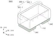
fig. 1 is a perspective view illustrating a multilayer electronic assembly according to an example embodiment of the present disclosure;
fig. 2 is a perspective view illustrating a main body of the multilayer electronic assembly in fig. 1;
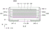
FIG. 3 is a cross-sectional view taken along line I-I' in FIG. 1;
fig. 4 is an exploded perspective view illustrating the main body in fig. 2;
fig. 5 is a perspective view showing a board assembly on which the multilayer electronic assembly of fig. 1 is mounted;
fig. 6 is a perspective view illustrating a multilayer electronic assembly according to an example embodiment of the present disclosure;
FIG. 7 is a cross-sectional view taken along line II-II' in FIG. 6;
fig. 8 is a perspective view illustrating a multilayer electronic assembly according to an example embodiment of the present disclosure;
FIG. 9 is a cross-sectional view taken along line III-III' in FIG. 8;
fig. 10 is a perspective view illustrating a multilayer electronic assembly according to an example embodiment of the present disclosure;
FIG. 11 is a cross-sectional view taken along line IV-IV' in FIG. 10;
fig. 12 is a perspective view illustrating a multilayer electronic assembly according to an example embodiment of the present disclosure;
FIG. 13 is a cross-sectional view taken along line V-V' in FIG. 12;
Fig. 14 is a perspective view illustrating a multilayer electronic assembly according to an example embodiment of the present disclosure;
FIG. 15 is a cross-sectional view taken along line VI-VI' in FIG. 14;
fig. 16 is a diagram showing a modified example of the example in fig. 14;
fig. 17 is a perspective view illustrating a multilayer electronic assembly according to an example embodiment of the present disclosure;
FIG. 18 is a cross-sectional view taken along line VII-VII' in FIG. 17;
fig. 19 is a perspective view illustrating a multilayer electronic assembly according to an example embodiment of the present disclosure;
FIG. 20 is a cross-sectional view taken along line VIII-VIII' in FIG. 19;
fig. 21 is a diagram showing a modified example of the example in fig. 19;
fig. 22 is a perspective view illustrating a multilayer electronic assembly according to an example embodiment of the present disclosure;
FIG. 23 is a cross-sectional view taken along line IX-IX' in FIG. 22;
fig. 24 is a diagram showing a modified example of the example in fig. 22;
fig. 25 is a perspective view illustrating a multilayer electronic assembly according to an example embodiment of the present disclosure;
FIG. 26 is a cross-sectional view taken along line X-X' in FIG. 25;
fig. 27 is a diagram showing a modified example of the example in fig. 25;
fig. 28 is a perspective view illustrating a multilayer electronic assembly according to an example embodiment of the present disclosure;
FIG. 29 is a cross-sectional view taken along line XI-XI' in FIG. 28;
Fig. 30 is a diagram showing a modified example of the example in fig. 28;
fig. 31 is a perspective view illustrating a multilayer electronic assembly according to an example embodiment of the present disclosure;
FIG. 32 is a cross-sectional view taken along line XII-XII' in FIG. 31;
fig. 33 is a perspective view illustrating a multilayer electronic assembly according to an example embodiment of the present disclosure;
FIG. 34 is a cross-sectional view taken along line XIII-XIII' in FIG. 33;
fig. 35 is a diagram showing a modified example of the example in fig. 33;
fig. 36 is a perspective view illustrating a multilayer electronic assembly according to an example embodiment of the present disclosure;
FIG. 37 is a cross-sectional view taken along line XIV-XIV' in FIG. 36; and
fig. 38 is an enlarged view showing a region K1 in fig. 37.
Detailed Description
Hereinafter, embodiments of the present disclosure will be described as follows with reference to the accompanying drawings.
This disclosure may, however, be embodied in many different forms and should not be construed as limited to the specific embodiments set forth herein. Rather, these embodiments are provided so that this disclosure will be thorough and complete, and will fully convey the scope of the disclosure to those skilled in the art. Accordingly, the shapes and sizes of elements in the drawings may be exaggerated for clarity of description. Furthermore, elements having the same function within the scope of the same concept presented in the drawings of each example embodiment will be described using the same reference numerals.
In the drawings, like elements will be denoted by like reference numerals. Furthermore, redundant descriptions and detailed descriptions of known functions and elements that may unnecessarily obscure the gist of the present disclosure will not be provided. In the drawings, some elements may be exaggerated, omitted, or briefly shown, and the sizes of the elements do not necessarily reflect the actual sizes of the elements. Furthermore, it will be understood that when a portion "comprises" an element, the portion can include other elements unless stated otherwise, without excluding other elements.
In the drawings, a first direction may be defined as a lamination direction or a thickness (T) direction, a second direction may be defined as a length (L) direction, and a third direction may be defined as a width (W) direction.
Fig. 1 is a perspective view illustrating a multilayer electronic assembly according to an example embodiment.
Fig. 2 is a perspective view illustrating a main body of the multilayer electronic assembly in fig. 1.
Fig. 3 is a sectional view taken along line I-I' in fig. 1.
Fig. 4 is an exploded perspective view illustrating the main body in fig. 2.
Fig. 5 is a perspective view showing a board assembly on which the multilayer electronic assembly of fig. 1 is mounted.
Hereinafter, a multilayer electronic component 1000 in an example embodiment will be described with reference to fig. 1 to 5.
The multilayer electronic assembly 1000 in an example embodiment may include: a body 110 including a dielectric layer 111 and first and second internal electrodes 121 and 122, the first and second internal electrodes 121 and 122 being alternately disposed with the dielectric layer 111 interposed between the first and second internal electrodes 121 and 122, and the body 110 having first and second surfaces 1 and 2 opposite to each other in a first direction, third and fourth surfaces 3 and 4 connected to the first and second surfaces 1 and 2 and opposite to each other in a second direction, and fifth and sixth surfaces 5 and 6 connected to the first and second and third and fourth surfaces 1 and 4 and 3 and 4 opposite to each other in a third direction; a first external electrode 131 including a first connection part 131a, a first tape part 131b, and a third tape part 131c, the first connection part 131a being disposed on the third surface, the first tape part 131b extending from the first connection part to a portion of the first surface, the third tape part 131c extending from the first connection part to a portion of the second surface; a second external electrode 132 including a second connection portion 132a, a second belt portion 132b, and a fourth belt portion 132c, the second connection portion 132a being disposed on the fourth surface, the second belt portion 132b extending from the second connection portion to a portion of the first surface, the fourth belt portion 132c extending from the second connection portion to a portion of the second surface; an insulating layer 151 disposed on the first and second connection parts and covering the second surface and the third and fourth belt parts 131c and 132c; a first plating layer 141 provided on the first belt portion 131 b; and a second plating layer 142 disposed on the second belt portion 132b, and the insulating layer 151 may include silicon (Si) -containing oxide.
In the body 110, the dielectric layer 111 and the internal electrodes 121 and 122 may be alternately laminated.
The shape of the body 110 may not be limited to any particular shape, but as shown, the body 110 may have a hexahedral shape or a shape similar to a hexahedral shape. The body 110 may not have an exact hexahedral shape formed of straight lines due to shrinkage of the ceramic powder included in the body 110 during the firing process, but may have a substantially hexahedral shape.
The body 110 may have: the first surface 1 and the second surface 2 are opposite to each other in the first direction; a third surface 3 and a fourth surface 4 connected to the first surface 1 and the second surface 2 and opposed to each other in the second direction; and fifth and sixth surfaces 5 and 6 connected to the first and second surfaces 1 and 2 and the third and fourth surfaces 3 and 4 and facing each other in the third direction.
In an example embodiment, the body 110 may have 1-3 corners connecting the first surface to the third surface, 1-4 corners connecting the first surface to the fourth surface, 2-3 corners connecting the second surface to the third surface, and 2-4 corners connecting the second surface to the fourth surface. The 1-3 and 2-3 corners may have a shape that tapers toward the center of the body in the first direction as it approaches the third surface, and the 1-4 and 2-4 corners may have a shape that tapers toward the center of the body in the first direction as it approaches the fourth surface.
Since the edge regions of the dielectric layer 111 where the internal electrodes 121 and 122 are not disposed are overlapped in the first direction, a step difference may be formed due to the thickness of the internal electrodes 121 and 122, and thus, corners connecting the first surface to the third surface and the fourth surface and/or corners connecting the second surface to the third surface and the fourth surface may have a form of being shrunk toward the center of the body in the first direction with respect to the first surface and/or the second surface. Alternatively, the corners connecting the first surface 1 to the third surface 3, the fourth surface 4, the fifth surface 5 and the sixth surface 6 and/or the corners connecting the second surface 2 to the third surface 3, the fourth surface 4, the fifth surface 5 and the sixth surface 6 may have a form of shrinking relative to the first surface and/or the second surface towards the center of the body in the first direction. Alternatively, when corners of the surfaces of the connection body 110 are rounded by performing a separate process to prevent peeling defects (peeling defects) or the like, corners connecting the first surface with the third surface to the sixth surface and/or corners connecting the second surface with the third surface to the sixth surface may have rounded shapes.
The corners may include 1-3 corners connecting the first surface to the third surface, 1-4 corners connecting the first surface to the fourth surface, 2-3 corners connecting the second surface to the third surface, and 2-4 corners connecting the second surface to the fourth surface. Further, the corners may include 1-5 corners connecting the first surface to the fifth surface, 1-6 corners connecting the first surface to the sixth surface, 2-5 corners connecting the second surface to the fifth surface, and 2-6 corners connecting the second surface to the sixth surface. The first to sixth surfaces of the body 110 may be substantially flat surfaces, and the non-flat region may be configured as a corner. Hereinafter, the extended line of each surface may refer to a line extending with respect to the flat portion of each surface.
In this case, in the external electrodes 131 and 132, regions disposed on corners of the body 110 may be corner portions, regions disposed on the third and fourth surfaces of the body 110 may be connection portions, and regions disposed on the first and second surfaces of the body may be band portions.
In order to prevent the step difference caused by the internal electrodes 121 and 122, after lamination, when the laminate is cut to expose the internal electrodes to both side surfaces of the capacitance forming portion Ac in the third direction (width direction), a single dielectric layer or two or more dielectric layers may be laminated on both side surfaces of the capacitance forming portion Ac in the third direction (width direction) to form edge portions 114 and 115, and a portion connecting the first surface to the fifth surface and a portion connecting the first surface to the sixth surface and a portion connecting the second surface to the fifth surface may not have a contracted form.
The plurality of dielectric layers 111 forming the body 110 may be in a fired state, and adjacent dielectric layers 111 may be integrated with each other, such that it is difficult to identify boundaries between adjacent dielectric layers 111 without using a Scanning Electron Microscope (SEM).
In the example embodiment, the raw material for forming the dielectric layer 111 is not limited to any particular example as long as a sufficient capacitance can be obtained. For example, a barium titanate material, a lead composite perovskite material, or a strontium titanate material may be used as a raw material for forming the dielectric layer 111. The barium titanate material may include BaTiO 3 Ceramic powder, and BaTiO 3 Examples of the ceramic powder may include one in which Ca (calcium), zr (zirconium) are partially solid-dissolved in BaTiO 3 (Ba) 1-x Ca x )TiO 3 (0<x<1)、Ba(Ti 1-y Ca y )O 3 (0<y<1)、(Ba 1-x Ca x )(Ti 1-y Zr y )O 3 (0<x<1、0<y<1) Or Ba (Ti) 1-y Zr y )O 3 (0<y<1)。
In addition, various ceramic additives, organic solvents, binders, dispersants, and the like may be added to the ceramic powder (such as barium titanate (BaTiO) 3 ) Ceramic powder) as a raw material for forming the dielectric layer 111 in the example embodiment.
The average thickness td of the dielectric layer 111 is not limited to any particular example.
However, in general, when the dielectric layer has a thickness of less than 0.6 μm (relatively thin), particularly when the thickness of the dielectric layer is 0.35 μm or less, reliability may be lowered.
In example embodiments, by providing an insulating layer on a connection portion of an external electrode and providing a plating layer on a tape portion of the external electrode, penetration of external moisture and plating solution may be prevented, and thus reliability may be improved. Therefore, even when the average thickness of the dielectric layer 111 is 0.35 μm or less, excellent reliability can be ensured.
Therefore, when the average thickness of the dielectric layer 111 is 0.35 μm or less, the effect of improving reliability in the example embodiment may be enhanced.
The average thickness td of the dielectric layer 111 may refer to an average thickness of the dielectric layer 111 disposed between the first and second internal electrodes 121 and 122.
The average thickness of the dielectric layer 111 may be measured by scanning a scan image obtained by scanning a cross-sectional surface of the body 110 taken in the length and thickness (L-T) directions at a magnification of 10000 using a Scanning Electron Microscope (SEM). More specifically, the average value can be measured by measuring the thickness of 30 points of the dielectric layer on the scanned image that are spaced apart by an equal distance in the length direction. 30 points spaced apart by equal distances may be specified in the capacitance forming portion Ac. Furthermore, when the measurement of the average value is extended to 10 dielectric layers and their average value is measured, the average thickness of the dielectric layers can be further generalized.
The body 110 may include: a capacitance forming portion Ac in which the first and second internal electrodes 121 and 122 are opposed to each other with the dielectric layer 111 interposed between the first and second internal electrodes 121 and 122; and covering portions 112 and 113 formed on upper and lower portions of the capacitance forming portion Ac in the first direction.
Further, the capacitance forming portion Ac may contribute to the capacitance formation of the capacitor, and may be formed by alternately layering a plurality of first internal electrodes 121 and a plurality of second internal electrodes 122 with the dielectric layer 111 interposed between the first internal electrodes 121 and the second internal electrodes 122.
The cover parts 112 and 113 may include: an upper cover 112 disposed above the capacitance forming portion Ac in the first direction; and a lower cover portion 113 provided below the capacitance forming portion Ac in the first direction.
The upper and lower cover parts 112 and 113 may be formed by stacking a single dielectric layer or two or more dielectric layers on the upper and lower surfaces of the capacitance forming part Ac, respectively, in the thickness direction, and damage to the internal electrode caused by physical stress and/or chemical stress may be prevented.
The upper and lower cover parts 112 and 113 do not include the inner electrode, and may include the same material as that of the dielectric layer 111.
That is, the upper and lower cladding portions 112, 113 may comprise a ceramic material (such as, for example, in titanic acidBarium (BaTiO) 3 ) Ceramic materials are examples).
The average thickness tc of the cover portions 112 and 113 is not limited to any particular example. However, in order to easily achieve miniaturization and high capacitance of the multilayer electronic component, the average thickness tc of the covering portions 112 and 113 may be 15 μm or less. Further, in the example embodiment, by providing an insulating layer on the connection portion of the external electrode and providing a plating layer on the band portion of the external electrode, penetration of external moisture and plating solution can be prevented, and thus reliability can be improved. Therefore, even when the average thickness tc of the covering portions 112 and 113 is 15 μm or less, excellent reliability can be ensured.
The average thickness tc of the cover portions 112 and 113 may refer to a dimension in the first direction, and may be an average of thicknesses of five points of the cover portions above or below the capacitance forming portion Ac that are spaced apart by an equal distance in the first direction. The average thickness may be measured by scanning a cross-sectional surface of the body 110 using a Scanning Electron Microscope (SEM). Other methods and/or tools known to those of ordinary skill in the art may be used, even if not described in the present disclosure.
Further, edge portions 114 and 115 may be provided on side surfaces of the capacitance forming portion Ac in the third direction.
The edge portions 114 and 115 may refer to: in a cross section of the body 110 taken in a width-thickness (W-T) direction, the first and second internal electrodes 121 and 122 have regions between both ends and a surface of the body.
The edge portions 114 and 115 may prevent damage to the internal electrode caused by physical stress and/or chemical stress.
The edge portions 114 and 115 may be formed by: when the internal electrode is formed by applying the conductive paste on the ceramic green sheet, the conductive paste is not applied on the region of the ceramic green sheet where the edge portion is to be formed.
Further, in order to prevent a step difference due to the internal electrodes 121 and 122, after lamination, the obtained laminated body may be cut to expose the internal electrodes to both side surfaces of the capacitance forming portion Ac in the third direction (width direction), and a single dielectric layer or two or more dielectric layers may be laminated on both side surfaces of the capacitance forming portion Ac in the third direction (width direction), thereby forming the edge portions 114 and 115.
The width of the edge portions 114 and 115 is not limited to any particular example. However, the average width of the edge portions 114 and 115 may be 15 μm or less to easily achieve miniaturization and high capacitance of the multilayer electronic component. Further, in the example embodiment, by providing an insulating layer on the connection portion of the external electrode and providing a plating layer on the band portion of the external electrode, penetration of external moisture and plating solution can be prevented, and thus reliability can be improved. Therefore, even when the average width of the edge portions 114 and 115 is 15 μm or less, excellent reliability can be ensured.
The average width of the edge portions 114 and 115 may refer to an average size of the edge portions 114 and 115 in the third direction, and may be an average value of thicknesses of five points of the edge portions 114 and 115 on the side surface of the capacitance forming portion Ac that are spaced apart by an equal distance in the third direction.
The internal electrodes 121 and 122 may be alternately laminated with the dielectric layer 111.
The internal electrodes 121 and 122 may include a first internal electrode 121 and a second internal electrode 122. The first and second internal electrodes 121 and 122 may be alternately disposed opposite to each other with the dielectric layer 111 interposed between the first and second internal electrodes 121 and 122, and the first and second internal electrodes 121 and 122 may be exposed to the third and fourth surfaces 3 and 4 of the body 110, respectively.
Referring to fig. 3, the first internal electrode 121 may be spaced apart from the fourth surface 4 and may be exposed through the third surface 3, and the second internal electrode 122 may be spaced apart from the third surface 3 and may be exposed through the fourth surface 4. The first external electrode 131 may be disposed on the third surface 3 of the body and may be connected to the first internal electrode 121, and the second external electrode 132 may be disposed on the fourth surface 4 of the body and may be connected to the second internal electrode 122.
That is, the first inner electrode 121 is not connected to the second outer electrode 132 but to the first outer electrode 131, and the second inner electrode 122 is not connected to the first outer electrode 131 but to the second outer electrode 132. Accordingly, the first inner electrode 121 may be spaced apart from the fourth surface 4 by a predetermined distance, and the second inner electrode 122 may be spaced apart from the third surface 3 by a predetermined distance.
In this case, the first and second internal electrodes 121 and 122 may be electrically separated from each other by the dielectric layer 111 disposed between the first and second internal electrodes 121 and 122.
The body 110 may be formed by: ceramic green sheets on which the conductive paste for the first internal electrodes 121 is printed and ceramic green sheets on which the conductive paste for the second internal electrodes 122 is printed are alternately laminated, and the green sheets are fired.
The material for forming the internal electrodes 121 and 122 is not limited to any particular example, and a material having excellent conductivity may be used. For example, the internal electrodes 121 and 122 may include one or more of nickel (Ni), copper (Cu), palladium (Pd), silver (Ag), gold (Au), platinum (Pt), tin (Sn), tungsten (W), titanium (Ti), and alloys thereof.
Further, the internal electrodes 121 and 122 may be formed by printing a conductive paste for the internal electrodes, including one or more of nickel (Ni), copper (Cu), palladium (Pd), silver (Ag), gold (Au), platinum (Pt), tin (Sn), tungsten (W), titanium (Ti), and alloys thereof. As a method of printing the conductive paste for the internal electrode, a screen printing method or a gravure printing method may be used, but is not limited thereto.
The average thickness te of the inner electrodes 121 and 122 is not limited to any particular example.
However, in general, when the internal electrode is formed to have a thickness (relatively thin) of less than 0.6 μm, reliability may be deteriorated, particularly when the thickness of the internal electrode is 0.35 μm or less.
In example embodiments, by providing an insulating layer on a connection portion of an external electrode and providing a plating layer on a tape portion of the external electrode, penetration of external moisture and plating solution may be prevented, and thus reliability may be improved. Therefore, even when the average thickness of the inner electrodes 121 and 122 is 0.35 μm or less, excellent reliability can be ensured.
Therefore, when the average thickness of the internal electrodes 121 and 122 is 0.35 μm or less, the effect in the example embodiment can be improved, and miniaturization and high capacitance of the ceramic electronic component can be easily obtained.
The average thickness te of the inner electrodes 121 and 122 may refer to the average thickness of the inner electrodes 121 and 122.
The average thickness of the inner electrodes 121 and 122 may be measured by scanning a scan image obtained by scanning a cross-sectional surface of the body 110 taken in the length and thickness (L-T) directions at a magnification of 10000 times using a Scanning Electron Microscope (SEM). More specifically, the average value can be measured by scanning an image to measure the thickness of 30 points of the inner electrode that are spaced apart by an equal distance in the length direction. 30 points spaced apart by equal distances may be specified in the capacitance forming portion Ac. Furthermore, when the measurement of the average value is extended to 10 internal electrodes and their average value is calculated, the average thickness of the internal electrodes can be further generalized.
The external electrodes 131 and 132 may be disposed on the third surface 3 and the fourth surface 4 of the body 110. The external electrodes 131 and 132 may include first and second external electrodes 131 and 132 disposed on the third and fourth surfaces 3 and 4 of the body 110, respectively, and connected to the first and second internal electrodes 121 and 122, respectively.
The external electrodes 131 and 132 may include: a first external electrode 131 including a first connection part 131a and a first tape part 131b, the first connection part 131a being disposed on the third surface, the first tape part 131b extending from the first connection part to a portion of the first surface; and a second external electrode 132 including a second connection portion 132a and a second belt portion 132b, the second connection portion 132a being disposed on the fourth surface, the second belt portion 132b extending from the second connection portion to a portion of the first surface. The first connection part 131a may be connected to the first internal electrode 121 on the third surface, and the second connection part 132a may be connected to the second internal electrode 122 on the fourth surface.
In addition, the first external electrode 131 may include a third band portion 131c extending from the first connection portion 131a to a portion of the second surface, and the second external electrode 132 may include a fourth band portion 132c extending from the second connection portion 132a to a portion of the second surface. In addition, the first external electrode 131 may include a first side tape part extending from the first connection part 131a to a portion of the fifth surface and a portion of the sixth surface, and the second external electrode 132 may include a second side tape part extending from the second connection part 132a to a portion of the fifth surface and a portion of the sixth surface.
However, in example embodiments, the third band portion, the fourth band portion, the first side band portion, and the second side band portion may not be provided. The first and second external electrodes 131 and 132 may not be disposed on the second surface, and may not be disposed on the fifth and sixth surfaces. When the first and second external electrodes 131 and 132 are not disposed on the second surface, the first and second external electrodes 131 and 132 may be disposed under an extension line of the second surface of the body. Further, the first and second connection parts 131a and 132a may be spaced apart from the fifth and sixth surfaces, and the first and second connection parts 131a and 132a may be spaced apart from the second surface. Further, the first and second belt portions 131b and 132b may also be spaced apart from the fifth and sixth surfaces.
When the first and second external electrodes 131 and 132 include the third and fourth band parts 131c and 132c, respectively, in example embodiments, an insulating layer may be formed on the third and fourth band parts 131c and 132c, but is not limited thereto. Plating may be provided on the third belt portion 131c and the fourth belt portion 132c to improve the ease of installation. In addition, the first and second external electrodes 131 and 132 may include the third and fourth band parts 131c and 132c, and may not include side band parts, and in this case, the first and second connection parts 131a and 132a and the first, second, third and fourth band parts 131b, 131c and 132c may be spaced apart from the fifth and sixth surfaces.
In an example embodiment, the multi-layered electronic assembly 1000 may have two external electrodes 131 and 132. However, the number of the external electrodes 131 and 132 and the shape thereof may be changed according to the shape of the internal electrodes 121 and 122 or other purposes.
The external electrodes 131 and 132 may be formed using any material having conductivity, such as metal, and a specific material may be determined in consideration of electrical properties and structural stability, and may have a multi-layered structure.
The external electrodes 131 and 132 may be fired electrodes including conductive metal and glass, or may be resin-based electrodes including conductive metal and resin.
In addition, the external electrodes 131 and 132 may have a shape in which a firing electrode and a resin-based electrode are sequentially formed on the body. Further, the external electrodes 131 and 132 may be formed by transferring a sheet including a conductive metal onto the body, or by transferring a sheet including a conductive metal onto the firing electrode.
As the conductive metal included in the external electrodes 131 and 132, a metal material having excellent conductivity may be used, and the metal material is not limited to any particular example. For example, the conductive metal may be one or more of Cu, ni, pd, ag, sn, cr and their alloys. Preferably, the external electrodes 131 and 132 may include at least one of Ni and a Ni alloy, and thus, connectivity with the internal electrodes 121 and 122 including Ni may be improved.
The insulating layer 151 may be disposed on the first and second connection parts 131a and 132 a.
Since the first and second connection parts 131a and 132a are directly connected to the internal electrodes 121 and 122, the first and second connection parts 131a and 132a may become paths through which plating solution may permeate in a plating process or through which moisture may permeate during actual use. In the example embodiment, since the insulating layer 151 is disposed on the connection parts 131a and 132a, penetration of external moisture or plating solution may be prevented.
The insulating layer 151 may be in contact with the first and second plating layers 141 and 142. In this case, the insulating layer 151 may be in contact with the end of the first plating layer 141 and the end of the second plating layer 142 and may partially cover the end of the first plating layer 141 and the end of the second plating layer 142, or the first plating layer 141 and the second plating layer 142 may be in contact with the end of the insulating layer 151 and may partially cover a portion of the end of the insulating layer 151.
The insulating layer 151 may be disposed on the first and second connection parts 131a and 132a, and may be disposed to cover the second surface and the third and fourth belt parts 131c and 132c. In this case, the insulating layer 151 may cover the third and fourth belt portions 131c and 132c and the region on the second surface where the third and fourth belt portions 131c and 132c are not disposed. Accordingly, the insulating layer 151 may cover the areas where the ends of the third and fourth belt parts 131c and 132c are in contact with the body 110, and may block a moisture penetration path, thereby improving moisture-proof reliability.
The insulating layer 151 may be disposed on the second surface, and may extend to the first and second connection parts 131a and 132a. Further, when the external electrodes 131 and 132 are not disposed on the second surface, the insulating layer may be disposed to entirely cover the second surface. The insulating layer does not have to be provided on the second surface, i.e., the insulating layer may not be provided on a part of the second surface or the entire second surface, and furthermore, the insulating layer may be divided into two parts, and the two parts may be provided on the first connection portion 131a and the second connection portion 132a, respectively. When the insulating layer is not disposed on the entire second surface, the insulating layer may be disposed under an extension line of the second surface. Further, the insulating layer may not be disposed on the second surface, and the insulating layer may extend from the first and second connection parts 131a and 132a to the fifth and sixth surfaces and may form one insulating layer.
Further, the insulating layer 151 may be provided to cover a portion of the first side band portion and a portion of the second side band portion, a portion of the fifth surface, and a portion of the sixth surface. In this case, portions of the fifth and sixth surfaces not covered by the insulating layer 151 may be exposed.
Further, the insulating layer 151 may be provided to cover the entire first and second side belt portions and the entire fifth and sixth surfaces, and in this case, the fifth and sixth surfaces may not be exposed, so that moisture-proof reliability may be improved. The connection parts 131a and 132a may not be directly exposed, thereby improving reliability of the multi-layered electronic assembly 1000. In more detail, the insulating layer may cover both the first and second side tape parts, and may cover the entire areas of the fifth and sixth surfaces except for the areas where the first and second side tape parts are formed.
The insulating layer 151 may prevent plating layers 141 and 142 from being formed on portions of the external electrodes 131 and 132 on which the insulating layer 151 is disposed, and may improve sealing properties, so that penetration of moisture or plating solution may be reduced.
The insulating layer may include silicon (Si) -containing oxide.
In order to mount a multilayer electronic component on a substrate, a solder reflow process may be required. In this process, as the temperature increases and decreases, thermal expansion and thermal reduction may occur, which may apply tensile stress to the multilayer electronic component. Such tensile stress may cause cracks in the multilayer electronic component, so that electrical properties may deteriorate.
In general, in order to protect the multilayer electronic component from thermal shock caused by thermal expansion and thermal reduction, an insulating layer (also referred to as a glass layer) may be formed using a glass-based material on a portion of the surface of the external electrode and a portion of the surface of the main body.
The insulating layer including a glass-based material may be formed by preparing glass powder or glass paste, and raising and lowering the temperature in the vicinity of the softening point. In this case, aggregation of the insulating layer may occur during a process of raising and lowering the temperature of the insulating layer, so that it may be difficult to form a uniform film. In addition, since the hardness of the insulating layer increases at a temperature lower than the softening point, and stress may be transmitted to the inside of the multilayer electronic component, cracks and delamination may occur in the multilayer electronic component. Furthermore, in the process of increasing temperature, metal in the outer electrode may diffuse into the inner electrode, which may cause radiation cracking. In particular, when the thickness of the insulating layer and the internal electrode is reduced in order to increase the capacitance and miniaturization of the multilayer electronic component, the multilayer electronic component may become susceptible to radiation cracking and delamination.
In example embodiments, the insulating layer 151 in the multilayer electronic component 1000 includes an Si-containing oxide, aggregation of the insulating layer can be prevented, and a uniform film can be formed, and stress transmitted to the inside of the multilayer electronic component 1000 can be prevented since hardness increases at low temperature (e.g., a temperature lower than a softening point of a conventional glass layer). Further, when the insulating layer including the Si-containing oxide is formed at a temperature lower than the softening point of the conventional glass layer, the metal in the external electrodes 131 and 132 can be prevented from diffusing into the internal electrodes 121 and 122, so that radiation cracks can be reduced.
Since the content of Si included in the insulating layer 151 is higher, penetration of external moisture can be effectively prevented and corrosion resistance to acid or alkali (such as plating solution) can be improved as compared with an insulating layer having the same thickness and formed using other materials.
In an example embodiment, in the insulating layer, a ratio of a mole number of Si to a mole number of an element other than oxygen may be 0.95 or more. That is, the insulating layer 151 may be formed substantially using an oxide containing Si, except for an element detected as an impurity.
The method of forming the insulating layer 151 including the Si-containing oxide may vary. For example, the insulating layer 151 may be formed by a sol-gel process, chemical Vapor Deposition (CVD), atomic Layer Deposition (ALD), or the like, but is not limited thereto, and the insulating layer 151 may be formed by another method for forming a uniform insulating layer.
The Si-containing oxide may be silicon dioxide (SiO 2 ). Silicon dioxide (SiO) 2 ) The insulating layer 151 may be formed thinner and more uniformly than a common glass-based material, and is formed with other inorganic materials (such as alumina (Al 2 O 3 ) And can have excellent impact resistance and corrosion resistance as compared with the conventional one.
In an example embodiment, the Si-containing oxide included in the insulating layer 151 may be silicon dioxide (SiO 2 ) Accordingly, the insulating layer 151 of the multilayer electronic assembly 1000 can be uniformly formed. Cracks and delamination can be prevented and radiation cracks can be prevented.
When the insulating layer 151 includes an oxide containing Si as in the multilayer electronic component 1000 in the example embodiment, each material included in the insulating layer may be unstable.
The boron-containing oxide may be mixed with other materials included in the insulating layerMaterials (e.g. SiO 2 ZnO, etc.) together to form a compound, thereby stabilizing the insulating layer. In example embodiments, the insulating layer 151 including Si-containing oxide may further include boron-containing oxide, and various materials may be organically combined, thereby improving stability of the insulating layer 151.
In particular, when the insulating layer 151 includes a boron-containing oxide, the boron-containing oxide may react with barium oxide on the surface of the body 110 at a low temperature, thereby forming a eutectic. Thus, in example embodiments, the multilayer electronic assembly 1000 may further include an adhesive layer including barium and boron at an interface between the insulating layer 151 (further including a boron-containing oxide) and the body 110, wherein the body 110 includes barium (Ba).
Since the material included in the insulating layer is, for example, siO 2 And B 2 O 3 And thus the adhesion with the first and second external electrodes 131 and 132 including the conductive metal may be poor. In the multilayer electronic assembly 1000 in the example embodiment, although the adhesion between the insulating layer 151 and the first and second external electrodes 131 and 132 is not good, the adhesion with the body 110 including the insulating material may be good, so that the overall strength of the multilayer electronic assembly 1000 may be improved.
More preferably, the boron-containing oxide included in the insulating layer 151 and the barium oxide included in the body 110 may form a eutectic bond at an interface between the insulating layer 151 and the body 110, and an adhesive layer including barium and boron may be formed, and thus, the overall strength of the multilayer electronic component 1000 may be improved.
In an example embodiment, the insulating layer 151 may further include a boron-containing oxide, and an adhesive layer including barium and boron may be further provided on an interface between the insulating layer 151 and the body 110. Accordingly, the adhesion between the insulating layer 151 and the body 110 may be improved, and the overall strength of the multilayer electronic assembly 1000 may be improved.
In this case, the composition of the insulating layer 151 can also be calculated by using an image observed by a scanning electron microscope-energy dispersive X-ray spectrometer (SEM-EDS). Specifically, the multilayer electronic component may be polished to a central position in the width direction (third direction), and a cross section (L-T cross section) taken in the length and thickness directions may be exposed, and in each of the regions obtained by dividing the insulating layer into 5 regions in the thickness direction, the type and the number of moles of each element included in the insulating layer may be measured using EDS, and the ratio of the number of moles of Si or the number of moles of boron to the total number of moles of elements other than oxygen may be calculated.
The multilayer electronic assembly 1000 in an example embodiment may include: a body 110 including a dielectric layer 111 and first and second internal electrodes 121 and 122, the first and second internal electrodes 121 and 122 being alternately disposed, and the dielectric layer 111 being based on between the first and second internal electrodes 121 and 122, and the body 110 having first and second surfaces 1 and 2 opposite to each other in a first direction, third and fourth surfaces 3 and 4 connected to the first and second surfaces 1 and 2 and opposite to each other in a second direction, and fifth and sixth surfaces 5 and 6 connected to the first and second and third and fourth surfaces 1 and 4 and 3 and 4 opposite to each other in a third direction; a first external electrode 131 including a first connection part 131a and a first tape part 131b, the first connection part 131a being disposed on the third surface, the first tape part 131b extending from the first connection part to a portion of the first surface; a second external electrode 132 including a second connection portion 132a and a second belt portion 132b, the second connection portion 132a being disposed on the fourth surface, the second belt portion 132b extending from the second connection portion to a portion of the first surface; an insulating layer 151 disposed on the second surface and extending to a portion of the first connection portion and a portion of the second connection portion; plating layers 141 and 142 are provided on first belt portion 131b and second belt portion 132 b. As an example, the insulating layer 151 may include at least one of boron (B) containing oxide, borosilicate, and zinc borosilicate.
In general, an insulating layer including a glass-based material may have a thermal expansion coefficient relatively greater than that of a main body or an external electrode, and may apply excessive stress to a multilayer electronic component.
When the insulating layer includes a boron-containing oxide, the insulating layer may be formed at a lower temperature than an insulating layer including a glass-based material, thereby preventing radiation cracks that may be generated in a process of forming the insulating layer, and the insulating layer may be formed by various methods such as a liquid and gas phase method.
Further, the insulating layer including the boron-containing oxide may have a lower thermal expansion coefficient than the insulating layer including the glass-based material, so that stress applied to the multilayer electronic component may be reduced even when the multilayer electronic component is heat-treated or thermal shock is applied from the outside, and since the insulating layer may have relatively improved physical impact resistance, the insulating layer may serve as a buffer layer to protect the multilayer electronic component.
In example embodiments, by configuring the insulating layer 151 to include a boron-containing oxide, reliability of the multilayer electronic component 1000 may be improved.
The boron-containing oxide may preferably utilize B 2 O 3 Formed, but is not limited thereto.
In an example embodiment, a ratio of a mole number of boron to a total mole number of elements other than oxygen in the insulating layer 151 may be 0.95 or more. That is, the insulating layer 151 may be formed substantially using a boron-containing oxide, except for an element detected as an impurity.
The borosilicate may have high corrosion resistance compared to boron-containing oxides, such that the borosilicate may serve as an insulating layer and may also protect the multilayer electronic component from penetration by plating solutions, and the borosilicate may have low moisture permeability. In the exemplary embodiment, since the insulating layer 151 includes borosilicate, moisture and plating solution may be prevented from penetrating into the multilayer electronic assembly 1000, thereby improving reliability.
In an example embodiment, a ratio of a mole number of boron and silicon to a total mole number of elements other than oxygen in the insulating layer 151 may be 0.95 or more. That is, the insulating layer 151 may be formed substantially using borosilicate, except for an element detected as an impurity.
Zinc borosilicate may be formed at a lower temperature than borosilicate, thereby further preventing radiation cracking, and wettability with a metal (such as Cu) included in the external electrode may be good.
In example embodiments, the insulating layer 151 includes zinc borosilicate, and thus radiation cracks may be prevented and a coupling force between the insulating layer 151 and the first and second external electrodes 131 and 132 may be improved. In addition, penetration of plating solution and moisture can be prevented by the improved bonding strength, thereby contributing to improvement of reliability of the multilayer electronic assembly 1000.
In an example embodiment, the ratio of the number of moles of boron, silicon, and zinc to the total number of moles of elements other than oxygen may be 0.95 or more in the insulating layer 151. That is, the insulating layer 151 may be formed substantially using zinc borosilicate, except for an element detected as an impurity.
The method of forming the insulating layer including at least one of boron-containing oxide, borosilicate, and zinc borosilicate may vary. For example, the insulating layer may be formed by a sol-gel process, chemical Vapor Deposition (CVD), atomic Layer Deposition (ALD), or the like, but is not limited thereto, and the insulating layer may be formed by another method for forming a uniform insulating layer.
In this case, the composition of the insulating layer 151 can be calculated by using an image observed by a scanning electron microscope-energy dispersive X-ray spectrometer (SEM-EDS). Specifically, the multilayer electronic component may be polished to a central position in the width direction (third direction), and a cross section (L-T cross section) taken in the length and thickness directions may be exposed, and the type and the number of moles of each element included in the insulating layer may be measured using EDS in each of the regions obtained by dividing the insulating layer into 5 regions in the thickness direction, and the ratio of the number of moles of Si or the number of moles of boron to the total number of moles of elements other than oxygen may be calculated.
In an example embodiment, the insulating layer 151 may include at least one of boron-containing oxide, borosilicate, and zinc borosilicate, and may further include various additives. By configuring the insulating layer 151 to include at least one of boron-containing oxide, borosilicate, and zinc borosilicate, stress applied to the multilayer electronic component 1000 due to external thermal shock can be reduced, so that cracks and delamination can be reduced, and radiation cracks can be prevented, and penetration of plating solution and external moisture can be prevented, so that reliability of the multilayer electronic component 1000 can be improved.
The first plating layer 141 and the second plating layer 142 may be provided on the first belt portion 131b and the second belt portion 132b, respectively. The plating layers 141 and 142 can improve the mounting performance, and when the plating layers 141 and 142 are provided on the belt portions 131b and 132b, the mounting space can be reduced, and also the penetration of the plating solution into the inner electrode can be reduced, so that the reliability can be improved. One end of the first plating layer 141 and one end of the second plating layer 142 may be in contact with the first surface, and the other end of the first plating layer 141 and the other end of the second plating layer 142 may be in contact with the insulating layer 151.
The types of the plating layers 141 and 142 are not limited to any particular example, and the plating layers 141 and 142 may be plating layers including at least one of Cu, ni, sn, ag, au, pd and an alloy thereof, and may include a plurality of layers.
As more specific examples of the plating layers 141 and 142, the plating layers 141 and 142 may be Ni plating layers or Sn plating layers, or may have a form in which Ni plating layers and Sn plating layers are sequentially formed on the first belt portion 131b and the second belt portion 132 b.
In an example embodiment, the first and second plating layers 141 and 142 may extend to partially cover the first and second connection parts 131a and 132a, respectively. When the average distance from the first surface 1 to the inner electrode disposed nearest to (closest to) the first surface 1 among the inner electrodes 121 and 122 in the first direction is defined as H1, and the average distance from the extension line E1 of the first surface 1 to the end portion of the first plating layer 141 disposed on the first connection portion 131a and the end portion of the second plating layer 142 disposed on the second connection portion 132a in the first direction is defined as H2, H1> H2 may be satisfied. Accordingly, the plating solution can be prevented from penetrating into the inner electrode during the plating process, thereby improving reliability.
H1 and H2 may be average values measured on sections (L-T sections) obtained by cutting in the first direction and the second direction at five points of the multilayer electronic assembly 1000 that are spaced apart by equal distances in the third direction. For example, measurements may be made by scanning a cross-section of the multilayer electronic assembly 1000 using a Scanning Electron Microscope (SEM). Other methods and/or tools known to those of ordinary skill in the art may be used, even if not described in the present disclosure. H1 may be an average value of values measured at a point of each section where an inner electrode disposed nearest to (closest to) the first surface 1 is connected to an outer electrode, H2 is an average value of values measured at an end portion of each section that is in contact with the outer electrode (e.g., a connection portion) with reference to the plating layer, and an extension line of the first surface as a reference may be the same when H1 and H2 are measured.
In an example embodiment, the first plating layer 141 may be disposed to cover an end portion of the insulating layer 151 disposed on the first external electrode 131, and the second plating layer 142 may be disposed to cover an end portion of the insulating layer 151 disposed on the second external electrode 132. Accordingly, cohesion (adhesion force) between the insulating layer 151 and the plating layers 141 and 142 can be enhanced, so that reliability of the multilayer electronic component 1000 can be improved.
In an example embodiment, the insulating layer 151 may be disposed to cover an end portion of the first plating layer 141 disposed on the first external electrode 131 and to cover an end portion of the second plating layer 142 disposed on the second external electrode 132. For example, the insulating layer 151 may be provided to cover an end portion of the first plating layer 141 provided on the first connection portion 131a, and to cover an end portion of the second plating layer 142 provided on the second connection portion 132 a. Accordingly, cohesion between the insulating layer 151 and the plating layers 141 and 142 can be enhanced, so that reliability of the multilayer electronic assembly 1000 can be improved.
Further, as shown in fig. 3, the insulating layer 151 may have an average thickness t2 substantially the same as the average thickness t1 of the first plating layer 141 and/or the second plating layer 142.
In an example embodiment, an average size of the body in the second direction is defined as L, an average distance from an extension line E3 of the third surface to an end of the first belt portion in the second direction is defined as B1, and an average distance from an extension line E4 of the fourth surface to an end of the second belt portion in the second direction is defined as B2, 0.2.ltoreq.b1/l.ltoreq.0.4 and 0.2.ltoreq.b2/l.ltoreq.0.4 may be satisfied.
When B1/L and B2/L are less than 0.2, it may be difficult to secure sufficient fixing strength. When B1/L and B2/L are greater than 0.4, leakage current may be generated between the first and second tape parts 131B and 132B at a high voltage current, and the first and second tape parts 131B and 132B may be electrically connected due to plating diffusion.
B1, B2, and L may be average values of values measured on sections (L-T sections) obtained by cutting in the first direction and the second direction at five points of the multilayer electronic assembly 1000 that are spaced apart by equal distances in the third direction. For example, measurements may be made by scanning a cross-section of the multilayer electronic assembly 1000 using a Scanning Electron Microscope (SEM). Other methods and/or tools known to those of ordinary skill in the art may be used, even if not described in the present disclosure.
Referring to fig. 5 showing the board assembly 1100 on which the multilayer electronic assembly 1000 is mounted, the plating layers 141 and 142 of the multilayer electronic assembly 1000 may be bonded to each other by the solders 191 and 192 and the electrode pads 181 and 182 provided on the substrate 180.
When the internal electrodes 121 and 122 are stacked in the first direction, the multi-layered electronic assembly 1000 may be horizontally mounted on the substrate 180 such that the internal electrodes 121 and 122 are parallel to the mounting surface. However, not limited to the horizontal mounting, and when the internal electrodes 121 and 122 are stacked in the third direction, the multilayer electronic assembly may be vertically mounted on the substrate such that the internal electrodes 121 and 122 may be perpendicular to the mounting surface.
The dimensions of the multilayer electronic assembly 1000 are not limited to any particular example.
However, in order to achieve both miniaturization and high capacitance, it may be necessary to increase the number of stacked layers by reducing the thickness of the dielectric layer and the internal electrode. Therefore, in a multilayer electronic component having a size of 1005 (length×width of 1.0mm×0.5 mm) or less, the effect of improving reliability and capacitance per unit volume in the example embodiment may be remarkable.
Therefore, when manufacturing errors, external electrode sizes, and the like are taken into consideration, the effect of improving reliability in the example embodiment may be enhanced when the length of the multilayer electronic assembly 1000 is 1.1mm or less and the width of the multilayer electronic assembly 1000 is 0.55mm or less. Here, the length of the multilayer electronic assembly 1000 may refer to the largest dimension of the multilayer electronic assembly 1000 in the second direction, and the width of the multilayer electronic assembly 1000 may refer to the largest dimension of the multilayer electronic assembly 1000 in the third direction. For example, the maximum size can be obtained by using an optical microscope. Other methods and/or tools known to those of ordinary skill in the art may be used, even if not described in the present disclosure.
Fig. 6 is a perspective view illustrating a multi-layered electronic assembly according to an example embodiment. Fig. 7 is a sectional view taken along line II-II' in fig. 6.
Referring to fig. 6 and 7, in the multilayer electronic assembly 1001 in an example embodiment, the first plating layer 141-1 and the second plating layer 142-1 may be disposed below an extension line E1 of the first surface. Therefore, the height of the solder can be reduced during mounting, and the mounting space can be reduced.
Further, the insulating layer 151-1 may extend to a region below an extension line of the first surface, and may be in contact with the first plating layer 141-1 and the second plating layer 142-1.
Fig. 8 is a perspective view illustrating a multi-layered electronic assembly according to an example embodiment. Fig. 9 is a sectional view taken along line III-III' in fig. 8.
Referring to fig. 8 and 9, the multilayer electronic assembly 1002 in an example embodiment may further include an additional insulating layer 161, the additional insulating layer 161 being disposed on the first surface 1 and between the first strap portion 131b and the second strap portion 132 b. Accordingly, leakage current that may occur between the first and second strap portions 131b and 132b under high voltage current can be prevented.
The type of the additional insulating layer 161 is not limited to any particular example. For example, similar to insulating layer 151, additional insulating layer 161 can include at least one of a Si-containing oxide, a boron-containing oxide, borosilicate, and zinc borosilicate. However, the additional insulating layer 161 and the insulating layer 151 may not need to be formed using the same material, and the additional insulating layer 161 and the insulating layer 151 may be formed using different materials. For example, the additional insulating layer 161 may include one or more polymer resins selected from epoxy resins, acrylic resins, and the like. In addition, the additional insulating layer 161 may include, in addition to the polymer resin, a material selected from the group consisting of TiO 2 、BaTiO 3 、Al 2 O 3 、SiO 2 And BaO as an additive. Thus, the combination with the main body or the body can be improvedAnd binding force of the external electrode.
Fig. 10 is a perspective view illustrating a multilayer electronic assembly according to an example embodiment. Fig. 11 is a sectional view taken along line IV-IV' in fig. 10.
Referring to fig. 10 and 11, in the multilayer electronic assembly 1003 according to the example embodiment, when an average distance from the first surface 1 to an inner electrode disposed nearest (closest) to the first surface 1 among the inner electrodes 121 and 122 in the first direction is defined as H1, and an average distance from an extension line E1 of the first surface 1 to an end portion of the first plating layer 141-3 disposed on the first connection portion 131a and an end portion of the second plating layer 142-3 disposed on the second connection portion 132a in the first direction is defined as H2, H1< H2 may be satisfied. Accordingly, the area in contact with the solder during mounting can be increased, and thus the bonding force can be improved.
More preferably, when the average size of the body 110 in the first direction is defined as T, H2< T/2 may be satisfied. That is, H1< H2< T/2 may be satisfied, which may be because the effect of improving moisture-proof reliability by the insulating layer may be reduced when H2 is T/2 or more.
H1, H2, and T may be average values of measured values on sections (L-T sections) obtained by cutting in the first direction and the second direction at five points of the multilayer electronic assembly 1003 that are spaced apart at equal distances in the third direction. For example, the measurement may be performed by scanning a cross section of the multilayer electronic assembly 1003 using a Scanning Electron Microscope (SEM). Other methods and/or tools known to those of ordinary skill in the art may be used, even if not described in the present disclosure. H1 may be an average value of values measured at a point of each section where an inner electrode disposed nearest to (closest to) the first surface 1 is connected to an outer electrode, H2 is an average value of values measured at an end portion of each section that is in contact with the outer electrode (e.g., a connection portion) with reference to the plating layer, and an extension line of the first surface as a reference may be the same when H1 and H2 are measured. Further, T may be an average value obtained by measuring the maximum size of the body 110 in the first direction in each section.
Further, as shown in fig. 10, the insulating layer 151-3 may cover the third and fourth belt portions 131c and 132c, a region on the second surface where the third and fourth belt portions 131c and 132c are not disposed, a portion of the first and second connection portions 131a and 132a, and a portion of the fifth surface and a portion of the sixth surface. Fig. 12 is a perspective view illustrating a multilayer electronic assembly 1004 according to an example embodiment. Fig. 13 is a sectional view taken along line V-V' in fig. 12.
Referring to fig. 12 and 13, in the multilayer electronic assembly 1004 in the example embodiment, the average length B1 of the first tape portion 131B-4 may be greater than the average length B3 of the third tape portion 131c-4, and the average length of the second tape portion 132B-4 may be greater than the average length B4 of the fourth tape portion 132 c-4. Accordingly, the area in contact with the solder during mounting can be increased, and thus the bonding force can be improved.
In more detail, an average distance from an extension line of the third surface 3 to an end of the first belt portion 131B-4 in the second direction is defined as B1, an average distance from an extension line of the fourth surface 4 to an end of the second belt portion 132B-4 in the second direction is defined as B2, an average distance from an extension line of the third surface 3 to an end of the third belt portion 131c-4 in the second direction is defined as B3, and an average distance from an extension line of the fourth surface 4 to an end of the fourth belt portion 132c-4 in the second direction is defined as B4, B3< B1 and B4< B2 can be satisfied.
In this case, when the average size of the body 110 in the second direction is defined as L, 0.2.ltoreq.B1/L.ltoreq.0.4 and 0.2.ltoreq.B2/L.ltoreq.0.4 may be satisfied.
B1, B2, B3, B4, and L may be average values of measured values on sections (L-T sections) obtained by cutting in the first direction and the second direction at five points of the multilayer electronic component 1004 that are spaced apart at equal distances in the third direction. For example, measurements may be made by scanning a cross-section of the multilayer electronic assembly 1004 using a Scanning Electron Microscope (SEM). Other methods and/or tools known to those of ordinary skill in the art may be used, even if not described in the present disclosure.
In addition, the first external electrode 131-4 may include a first side tape part extending from the first connection part 131a-4 to a portion of the fifth surface and a portion of the sixth surface, and the second external electrode 132-4 may include a second side tape part extending from the second connection part 132a-4 to a portion of the fifth surface and a portion of the sixth surface. In this case, the dimensions of the first side belt portion and the second side belt portion in the second direction may gradually increase toward the first surface in the first direction. That is, the first side belt portion and the second side belt portion may be provided in a tapered shape or a trapezoidal shape.
Further, when the average distance from the extension line of the third surface to the end of the third band portion 131c-4 in the second direction is defined as B3, the average distance from the extension line of the fourth surface to the end of the fourth band portion 132c-4 in the second direction is defined as B4, the average size measured in the second direction of the area where the third surface and the second internal electrode 122 are spaced apart from each other is defined as G1, and the average size measured in the second direction of the area where the fourth surface and the first internal electrode 121 are spaced apart from each other is defined as G2, B3 ∈g1 and B4 ∈g2 may be satisfied. Accordingly, the volume occupied by the external electrodes can be reduced, and thus the capacitance per unit volume of the multilayer electronic component 1004 can be increased.
For G1 and G2, on a cross section obtained by cutting the main body in the first direction and the second direction at the center taken in the third direction, an average value of the dimensions in the second direction of the region spaced apart from the third surface measured with respect to any five of the second inner electrodes disposed in the center taken in the first direction may be G1, and on a cross section obtained by cutting the main body in the first direction and the second direction at the center taken in the third direction, an average value of the dimensions in the second direction of the region spaced apart from the fourth surface measured with respect to any five of the first inner electrodes disposed in the center taken in the first direction may be G2. For example, the measurement may be performed by scanning a cross section of the body 110 using a Scanning Electron Microscope (SEM). Other methods and/or tools known to those of ordinary skill in the art may be used, even if not described in the present disclosure.
Further, G1 and G2 may be obtained from a cross section (L-T cross section) obtained by cutting the main body 110 in the first direction and the second direction at five points spaced apart at equal distances in the third direction, and G1 and G2 may be average values, so that these values may be further generalized.
However, the present disclosure is not limited to B3.ltoreq.G1 and B4.ltoreq.G2, and may include examples satisfying B3.gtoreq.G1 and B4.gtoreq.G2 as example embodiments. Thus, in the example embodiment, when the average distance from the extension line of the third surface to the end of the third strip portion in the second direction is defined as B3, the average distance from the extension line of the fourth surface to the end of the fourth strip portion in the second direction is defined as B4, the average size measured in the second direction of the region where the third surface and the second inner electrode are spaced apart from each other is defined as G1, and the average size measured in the second direction of the region where the fourth surface and the first inner electrode are spaced apart from each other is defined as G2, B3 ≡g1 and B4 ≡g2 may be satisfied.
In an example embodiment, when an average distance from an extension line E3 of the third surface to an end of the first belt portion in the second direction is defined as B1, and an average distance from an extension line of the fourth surface to an end of the second belt portion in the second direction is defined as B2, B1 Σg1 and B2 Σg2 may be satisfied. The bonding force of the multilayer electronic component 1004 to the substrate 180 can be improved.
Fig. 14 is a perspective view illustrating a multilayer electronic assembly 1005 according to an example embodiment. Fig. 15 is a sectional view taken along line VI-VI' in fig. 14.
Referring to fig. 14 and 15, the first and second external electrodes 131-5 and 132-5 of the multilayer electronic assembly 1005 in example embodiments may not be disposed on the second surface, and may be disposed on the third and first surfaces, and the fourth and first surfaces, respectively, and may have L-shapes, respectively. That is, the first and second external electrodes 131-5 and 132-5 may be disposed under the extension line E2 of the second surface.
The first external electrode 131-5 may include a first connection part 131a-5 disposed on the third surface 3 and a first strap part 131b-5 extending from the first connection part 131a-5 to a portion of the first surface 1. The second external electrode 132-5 may include a second connection portion 132a-5 provided on the fourth surface 4 and a second belt portion 132b-5 extending from the second connection portion 132a-5 to a portion of the first surface 1. The external electrodes 131-5 and 132-5 may not be disposed on the second surface 2, so that the insulating layer 151-5 may be disposed to cover the entire second surface 2. Accordingly, the volume occupied by the external electrodes 131-5 and 132-5 can be reduced, so that the capacitance per unit volume of the multilayer electronic assembly 1005 can be improved. However, the present disclosure is not limited to an example in which the insulating layer 151-5 covers the entire second surface 2, and the insulating layer may not cover a portion of the second surface 2 or the entire second surface 2, and may be separated from the second surface 2, and may cover the first connection portion 131a-5 and the second connection portion 132a-5.
Further, the insulating layer 151-5 may be provided to cover a portion of the fifth surface and a portion of the sixth surface, thereby improving reliability. In this case, portions of the fifth and sixth surfaces not covered by the insulating layer 151-5 may be exposed.
Further, the insulating layer 151-5 may be provided to cover the entire fifth surface and the entire sixth surface, and in this case, the fifth surface and the sixth surface may not be exposed, so that moisture-proof reliability may be improved.
The first plating layer 141-5 may be disposed on the first belt portion 131b-5, the second plating layer 142-5 may be disposed on the second belt portion 132b-5, and the first and second plating layers 141-5 and 142-5 may extend to a portion of the first and second connection portions 131a-5 and 132b-5, respectively.
In this case, the external electrodes 131-5 and 132-5 may not be disposed on the fifth surface 5 and the sixth surface 6. That is, the external electrodes 131-5 and 132-5 may be disposed only on the third surface, the fourth surface, and the first surface.
An average distance from the first surface 1 to an inner electrode disposed nearest (closest) to the first surface 1 among the first inner electrode 121 and the second inner electrode 122 in the first direction is defined as H1, and an average distance from an extension line E1 of the first surface 1 to an end portion of the first plating layer 141-5 disposed on the first connection portion 131a-5 and an end portion of the second plating layer 142-5 disposed on the second connection portion 132a-5 in the first direction is defined as H2, H1< H2 may be satisfied. Accordingly, a region in contact with solder during mounting can be increased, so that bonding force can be improved, and an area where the external electrodes 131-5 and 132-5 and the plating layers 141-5 and 142-5 contact each other can be increased, so that an increase in Equivalent Series Resistance (ESR) can be prevented.
More preferably, when the average size of the body 110 in the first direction is defined as T, H2< T/2 may be satisfied. That is, H1< H2< T/2 may be satisfied, which may be because the effect of improving moisture-proof reliability by the insulating layer may be reduced when H2 is T/2 or more.
Further, the first plating layer 141-5 and the second plating layer 142-5 may be provided to cover a portion of the insulating layer 151-5 on the third surface and the fourth surface. That is, the plating layers 141-5 and 142-5 may be disposed to cover the ends of the insulating layer 151-5 on the third surface and the fourth surface. Accordingly, the bonding force between the insulating layer 151-5 and the plating layers 141-5 and 142-5 can be enhanced, so that the reliability of the multilayer electronic component 1005 can be improved.
Further, the insulating layer 151-5 may be provided so as to cover a portion of the first plating layer 141-5 on the third surface and a portion of the second plating layer 142-5 on the fourth surface. That is, the insulating layer 151-5 may be provided to cover the ends of the plating layers 141-5 and 142-5 on the third surface and the fourth surface. Accordingly, the bonding force between the insulating layer 151-5 and the plating layers 141-5 and 142-5 can be enhanced, so that the reliability of the multilayer electronic component 1005 can be improved.
Fig. 16 is a diagram showing a modified example of the example in fig. 14. Referring to fig. 16, in a multilayer electronic component 1006 of a modified example of the multilayer electronic component 1005 in the example embodiment, a first additional electrode layer 134 may be provided between the first connection portion 131a-6 and the third surface. A second additional electrode layer 135 may be disposed between the second connection portion 132a-6 and the fourth surface. The first additional electrode layer 134 may be disposed in a range not deviating from the third surface, and the second additional electrode layer 135 may be disposed in a range not deviating from the fourth surface. The first and second additional electrode layers 134 and 135 may improve electrical connectivity between the inner electrodes 121 and 122 and the outer electrodes 131-6 and 132-6, and bonding strength with the outer electrodes 131-6 and 132-6 may be excellent, so that mechanical bonding strength with the outer electrodes 131-6 and 132-6 may be further improved.
The first external electrode 131-6 may have an L-shape in which the first external electrode is not disposed on the second surface, and the second external electrode 132-6 may have an L-shape in which the second external electrode is not disposed on the second surface.
The first external electrode 131-6 may include a first connection part 131a-6 disposed on the first additional electrode layer 134 and a first tape part 131b-6 extending from the first connection part 131a-6 to a portion of the first surface 1. The second external electrode 132-6 may include a second connection portion 132a-6 disposed on the second additional electrode layer 135 and a second band portion 132b-6 extending from the second connection portion 132a-6 to a portion of the first surface 1.
The first and second additional electrode layers 134 and 135 may be formed using any material having conductivity, such as metal, and a specific material may be determined in consideration of electrical properties, structural stability, and the like. Further, the first additional electrode layer 134 and the second additional electrode layer 135 may be firing electrodes including conductive metal and glass, or may be resin-based electrodes including conductive metal and resin. Further, the first additional electrode layer 134 and the second additional electrode layer 135 may be formed by transferring a sheet including a conductive metal to the body.
As the conductive metal included in the first additional electrode layer 134 and the second additional electrode layer 135, a metal material having excellent conductivity may be used, and the metal material is not limited to any particular example. For example, the conductive metal may be one or more of Cu, ni, pd, ag, sn, cr and their alloys. Preferably, the first and second additional electrode layers 134 and 135 may include at least one of Ni and a Ni alloy, and thus, connectivity with the inner electrodes 121 and 122 including Ni may be further improved.
Fig. 17 is a perspective view illustrating a multilayer electronic assembly 1007 according to an example embodiment. Fig. 18 is a sectional view taken along line VII-VII' in fig. 17.
Referring to fig. 17 and 18, the average thickness t1 of the first and second plating layers 141-6 and 142-6 of the multilayer electronic assembly 1007 in example embodiments may be less than the average thickness t2 of the insulating layer 151-6.
The insulating layer 151-6 may prevent penetration of external moisture or plating solution, but the connectivity with the plating layers 141-6 and 142-6 may be relatively weak, which may cause delamination of the plating layers. When the plating layer is delaminated, the bonding force with the substrate 180 may be reduced. Here, delamination of the plating layers 141-6 and 142-6 may refer to partial detachment of the plating layers or physical separation of the plating layers from the external electrodes 131-5 and 132-5. Since the connectivity between the plating layer and the insulating layer is relatively weak, it is highly likely that the gap between the insulating layer and the plating layer may be widened or foreign matter may enter, which results in the plating layer being susceptible to external impact, and thus the possibility of delamination may increase.
In example embodiments, by reducing the average thickness t1 of the plating layer to be smaller than the average thickness t2 of the insulating layer, the contact area between the plating layer and the insulating layer may be reduced, thereby preventing delamination and improving the bonding force of the multilayer electronic assembly 1007 to the substrate 180.
The thickness t1 of the first and second plating layers 141-6 and 142-6 may be an average value of thicknesses at 5 points spaced apart by an equal distance of the first and second connection parts 131a-5 and 132a-5 or the first and second belt parts 131b-5 and 132b-5, and the thickness t2 of the insulating layer 151-6 may be an average value of thicknesses at 5 points spaced apart by an equal distance of the first and second connection parts 131a-5 and 132 a-5.
Fig. 19 is a perspective view illustrating a multi-layered electronic assembly 2000 according to an example embodiment. Fig. 20 is a cross-sectional view taken along line VIII-VIII' in fig. 19.
Hereinafter, the multilayer electronic assembly 2000 according to the example embodiment will be described, and a description repeated with the above-described example embodiment will not be provided.
The multilayer electronic assembly 2000 in an example embodiment may include: a body 110 including a dielectric layer 111 and first and second internal electrodes 121 and 122, the first and second internal electrodes 121 and 122 being alternately disposed with the dielectric layer 111 interposed between the first and second internal electrodes 121 and 122, and the body 110 having first and second surfaces 1 and 2 opposite to each other in a first direction, third and fourth surfaces 3 and 4 connected to the first and second surfaces 1 and 2 and opposite to each other in a second direction, and fifth and sixth surfaces 5 and 6 connected to the first and second and third and fourth surfaces 1 and 4 and 3 and 4 opposite to each other in a third direction; a first external electrode 231 including a first connection electrode 231a and a first strap electrode 231b, the first connection electrode 231a being disposed on the third surface, the first strap electrode 231b being disposed on the first surface and connected to the first connection electrode; a second external electrode 232 including a second connection electrode 232a and a second belt electrode 232b, the second connection electrode 232a being disposed on the fourth surface, the second belt electrode 232b being disposed on the first surface and connected to the second connection electrode; a first insulating layer 251 disposed on the first connection electrode; a second insulating layer 252 disposed on the second connection electrode; a first plating layer 241 provided on the first electrode; and a second plating layer 242 provided on the second electrode. As an example, the first insulating layer 251 and the second insulating layer 252 may include silicon (Si) -containing oxide.
The first connection electrode 231a may be disposed on the third surface 3 and may be connected to the first internal electrode 121, and the second connection electrode 232a may be disposed on the fourth surface 4 and may be connected to the second internal electrode 122. Further, the first insulating layer 251 may be disposed on the first connection electrode 231a, and the second insulating layer 252 may be disposed on the second connection electrode 232 a.
In general, when forming the external electrode, a method of immersing the surface of the body exposing the internal electrode in a paste including a conductive metal may be mainly used. However, the thickness of the external electrode formed by the dipping method may be excessively large in the central portion thereof in the thickness direction. Further, since the inner electrode is exposed to the third surface and the fourth surface except for the uneven thickness of the outer electrode by using the dipping method, the thickness of the outer electrode disposed on the third surface and the fourth surface may be equal to or greater than a predetermined thickness in order to prevent penetration of moisture and plating solution through the outer electrode.
Unlike the above example, in the example embodiment, since the insulating layers 251 and 252 are provided on the connection electrodes 231a and 232a, sufficient reliability can be ensured even when the thicknesses of the connection electrodes 231a and 232a on the third surface and the fourth surface are reduced.
The first and second connection electrodes 231a and 232a may have shapes corresponding to the third and fourth surfaces, respectively, and surfaces of the first and second connection electrodes 231a and 232a facing the main body 110 may have the same area as the third and fourth surfaces of the main body 110. The first connection electrode 231a and the second connection electrode 232a may be disposed within a range not deviating from the third surface 3 and the fourth surface 4, respectively. The connection electrodes 231a and 232a may be disposed not to extend to the first surface 1, the second surface 2, the fifth surface 5, and the sixth surface 6 of the body 110. In particular, in the example embodiment, the first and second connection electrodes 231a and 232a may be spaced apart from the fifth and sixth surfaces, and thus, sufficient connection between the inner electrodes 121 and 122 and the outer electrodes 231 and 232 may be ensured, and the volume occupied by the outer electrodes may be reduced, so that the capacitance per unit volume of the multilayer electronic assembly 2000 may be increased.
In this regard, the first connection electrode 231a and the second connection electrode 232a may be spaced apart from the second surface 2. That is, since the external electrodes 231 and 232 are not disposed on the second surface, the volume occupied by the external electrodes 231 and 232 may be further reduced, and thus the capacitance per unit volume of the multilayer electronic assembly 2000 may be increased.
The connection electrodes 231a and 232a may extend to corners of the body 110, and may include corner portions disposed on the corners. That is, in an example embodiment, the first connection electrode may include corner portions (not shown) extending to 1-3 corners and 2-3 corners, and the second connection electrode may include corner portions (not shown) extending to 1-4 corners and 2-4 corners.
In addition, the connection electrodes 231a and 232a may have a uniform and reduced thickness as compared to external electrodes formed by a conventional dipping method.
The method of forming the connection electrodes 231a and 232a is not limited to any particular example, for example, the connection electrodes 231a and 232a may be formed by a method of transferring a sheet including a conductive metal or an organic material (such as an adhesive) to the third surface and the fourth surface, but is not limited thereto, and the connection electrodes 231a and 232a may be formed by plating a conductive metal on the third surface and the fourth surface. That is, the connection electrodes 231a and 232a may be plating layers or firing layers formed by firing conductive metals.
The thickness of the connection electrodes 231a and 232a is not limited to any particular example, and may be, for example, 2 μm to 7 μm. Here, the thickness of the connection electrodes 231a and 232a may indicate the maximum thickness, and may represent the size of the connection electrodes 231a and 232a in the second direction.
In an example embodiment, the first and second connection electrodes 231a and 232a may include glass and the same metal as that included in the inner electrodes 121 and 122. Since the first and second connection electrodes 231a and 232a include the same metal as that included in the inner electrodes 121 and 122, electrical connectivity with the inner electrodes 121 and 122 may be improved, and since the first and second connection electrodes 231a and 232a include glass, bonding strength with the main body 110 and/or the insulating layers 251 and 252 may be improved. In this case, the same metal as that included in the inner electrodes 121 and 122 may be Ni.
The first insulating layer 251 and the second insulating layer 252 may be disposed on the first connection electrode 231a and the second connection electrode 232a, respectively, and may prevent plating layers from being formed on the first connection electrode 231a and the second connection electrode 232a, respectively. In addition, the first insulating layer 251 and the second insulating layer 252 may improve sealing performance, thereby reducing penetration of moisture or plating solution.
In an example embodiment, the first insulating layer 251 and the second insulating layer 252 may include silicon (Si) -containing oxide. Therefore, moisture-proof reliability can be improved, and cracks due to heat shrinkage and radiation cracks due to metal diffusion can be prevented.
In this case, in example embodiments, the first and second insulating layers 251 and 252 may further include a boron-containing oxide, and an adhesive layer including barium and boron may be further provided on an interface between the first insulating layer 251 and the main body 110 and an interface between the second insulating layer 252 and the main body 110, so that adhesion between the insulating layers 251 and 252 and the main body 110 may be improved, and overall strength of the multilayer electronic assembly 2000 may be improved.
In an example embodiment, in the first insulating layer 251 and the second insulating layer 252, a ratio of a mole number of Si to a mole number of an element other than oxygen may be 0.95 or more. That is, the first insulating layer 251 and the second insulating layer 252 may be formed substantially using an Si-containing oxide, except for an element detected as an impurity, and thus, penetration of external moisture may be effectively prevented, and moisture-proof reliability and corrosion resistance to acid or alkali (such as plating solution) may be improved, as compared with an insulating layer including different components and having the same thickness.
Further, in an example embodiment, the first insulating layer 251 and the second insulating layer 252 may include at least one of boron-containing oxide, borosilicate, and zinc borosilicate. Accordingly, by reducing stress applied to the multilayer electronic assembly 2000 due to external thermal shock, cracks and delamination may be reduced, radiation cracks may be prevented, and penetration of plating solution and external moisture may be prevented, so that reliability of the multilayer electronic assembly 2000 may be improved.
In the above-described example embodiments, the first and second insulating layers 251 and 252 include at least one of boron-containing oxide, borosilicate, and zinc borosilicate, which may react with barium oxide on the surface of the body 110 at low temperature, and may form a eutectic. Thus, in an example embodiment, the multilayer electronic assembly 2000 may further include an adhesion layer comprising barium and boron at the interface between the insulating layers 251 and 252 (further comprising boron-containing oxide) and the body 110.
Since the material included in the insulating layer is, for example, siO 2 And B 2 O 3 And thus the adhesion with the first and second external electrodes 231 and 232 including the conductive metal may be poor. In the multilayer electronic assembly 2000 in the example embodiment, although the adhesion between the insulating layers 251 and 252 and the first and second external electrodes 231 and 232 is not good, the adhesion with the body 110 including the insulating material may be good, so that the overall strength of the multilayer electronic assembly 2000 may be improved.
The first belt electrode 231b and the second belt electrode 232b may be disposed on the first surface 1 of the body 110. The first belt electrode 231b and the second belt electrode 232b may be electrically connected to the first and second inner electrodes 121 and 122, respectively, by being in contact with the first and second connection electrodes 231a and 232a, respectively.
The thicknesses of the external electrodes formed by the conventional dipping method may be formed to be relatively large on the third and fourth surfaces and may partially extend to the first, second, fifth and sixth surfaces, so that it may be difficult to secure a high effective volume ratio.
In example embodiments, the first connection electrode 231a and the second connection electrode 232a may be disposed on a surface on which the inner electrode is exposed, and the first belt electrode 231b and the second belt electrode 232b may be disposed on a mounting surface of the multi-layered electronic component, so that a high effective volume ratio may be ensured.
When the internal electrodes 121 and 122 are stacked in the first direction, the multilayer electronic assembly 2000 may be horizontally mounted on the substrate such that the internal electrodes 121 and 122 may be parallel to the mounting surface. However, not limited to the horizontal mounting, and when the internal electrodes 121 and 122 are stacked in the third direction, the multilayer electronic assembly may be vertically mounted on the substrate such that the internal electrodes 121 and 122 may be perpendicular to the mounting surface.
The first belt electrode 231b and the second belt electrode 232b may be formed using any material having conductivity (such as metal), and a specific material may be determined in consideration of electrical properties and structural stability. For example, the first and second belt electrodes 231b and 232b may be firing electrodes including conductive metal and glass, and may be formed by applying paste including conductive metal and glass to the first surface of the body, but are not limited thereto, and the first and second belt electrodes 231b and 232b may be plating layers formed by plating conductive metal on the first surface of the body.
As the conductive metal included in the first belt electrode 231b and the second belt electrode 232b, a metal material having excellent conductivity may be used, and the metal material is not limited to any particular example. For example, the conductive metal may be one or more of nickel (Ni), copper (Cu), and alloys thereof, and may include the same metal as that included in the inner electrodes 121 and 122.
In an example embodiment, in order to ensure sealing performance and high strength, the first external electrode 231 may include a third band electrode (not shown) disposed on the second surface 2 and connected to the first connection electrode 231a, and the second external electrode 232 may include a fourth band electrode (not shown) disposed on the second surface 2 and connected to the second connection electrode 232 a.
In an example embodiment, a distance from an extension line E3 of the third surface to an end of the first band electrode 231B in the second direction is defined as B1, a distance from an extension line E4 of the fourth surface to an end of the second band electrode 232B in the second direction is defined as B2, a distance from an extension line of the third surface to an end of the third band electrode (not shown) in the second direction is defined as B3, a distance from an extension line of the fourth surface to an end of the fourth band electrode (not shown) in the second direction is defined as B4, an average size measured in the second direction of a region where the third surface and the second inner electrode 122 are spaced apart from each other is defined as G1, and an average size measured in the second direction of a region where the fourth surface and the first inner electrode 121 are spaced apart from each other is defined as G2, B1, B3G 1, B2G 2 and B4G 2 may be satisfied. Accordingly, the volume occupied by the external electrodes may be reduced, so that the capacitance per unit volume of the multilayer electronic assembly 2000 may be increased, and the area in contact with solder during mounting may be increased, thereby improving bonding force.
However, the present disclosure is not limited to B1. Gtoreq.G1, B3. Gtoreq.G1, B2. Gtoreq.G2, and B4. Gtoreq.G2, and examples that satisfy B1. Gtoreq.G1, B3. Gtoreq.G1, B2. Gtoreq.G2, and B4. Gtoreq.G2 may be included in example embodiments. Thus, in the example embodiment, the distance from the extension line E3 of the third surface to the end of the first strip electrode 231B in the second direction is defined as B1, the distance from the extension line E4 of the fourth surface to the end of the second strip electrode 232B in the second direction is defined as B2, the distance from the extension line of the third surface to the end of the third strip electrode (not shown) in the second direction is defined as B3, the distance from the extension line of the fourth surface to the end of the fourth strip electrode (not shown) in the second direction is defined as B4, the average size measured in the second direction of the region where the third surface and the second inner electrode 122 are spaced apart from each other is defined as G1, and the average size in the second direction of the region where the fourth surface and the first inner electrode 121 are spaced apart from each other is defined as G2, B1. Gtoreq G1, B3. Gtoreq.g2 and B4. Gtoreq.g2 may be satisfied.
The first and second plating layers 241 and 242 may be disposed on the first and second belt electrodes 231b and 232b, respectively. The first plating layer 241 and the second plating layer 242 may improve the mounting performance. The types of the first plating layer 241 and the second plating layer 242 are not limited to any particular example, and the first plating layer 241 and the second plating layer 242 may be plating layers including at least one of Ni, sn, pd, and alloys thereof, and may include a plurality of layers.
For example, the first and second plating layers 241 and 242 may be Ni plating layers or Sn plating layers, or may have a form in which Ni plating layers and Sn plating layers are sequentially formed on the first and second belt electrodes 231b and 232 b.
In an example embodiment, the first and second plating layers 241 and 242 may extend to partially cover the first and second connection electrodes 231a and 232a, respectively.
When the average distance from the first surface 1 to the inner electrode disposed nearest (closest) to the first surface 1 among the first inner electrode 121 and the second inner electrode 122 in the first direction is defined as H1, and the average distance from the extension line E1 of the first surface 1 to the end portion of the first plating layer 241 disposed on the first connection electrode 231a and the end portion of the second plating layer 242 disposed on the second connection electrode 232a in the first direction is defined as H2, H1> H2 may be satisfied. Accordingly, the plating solution can be prevented from penetrating into the inner electrode during the plating process, thereby improving reliability.
In an example embodiment, the first and second insulating layers 251 and 252 may be disposed in direct contact with the first and second connection electrodes 231a and 232a, respectively, and the first and second connection electrodes 231a and 232a may include conductive metal and glass. Accordingly, since the plating layers 241 and 242 may not be disposed on the regions provided with the insulating layers 251 and 252 among the outer surfaces of the first and second connection electrodes 231a and 232a, erosion of the external electrodes caused by the plating solution may be effectively prevented.
In an example embodiment, the first and second insulating layers 251 and 252 may be disposed in direct contact with the first and second connection electrodes 231a and 232a, respectively, and the first and second connection electrodes 231a and 232a may include conductive metals and resins. Accordingly, since the plating layers 241 and 242 may not be disposed on the regions provided with the insulating layers 251 and 252 among the outer surfaces of the first and second connection electrodes 231a and 232a, erosion of the external electrodes caused by the plating solution may be effectively prevented.
In an example embodiment, the first plating layer 241 may be disposed to cover an end portion of the first insulating layer 251 disposed on the first external electrode 231, and the second plating layer 242 may be disposed to cover an end portion of the second insulating layer 252 disposed on the second external electrode 232. Accordingly, the coupling force between the insulating layers 251 and 252 and the plating layers 241 and 242 may be reinforced, so that the reliability of the multilayer electronic assembly 2000 may be improved. Further, by first forming the first insulating layer 251 and the second insulating layer 252 before forming the plating layers 241 and 242 on the external electrodes 231 and 232, penetration of the plating solution can be reliably prevented in the process of forming the plating layers. Since the insulating layers are formed before plating, the plating layers 241 and 242 may have a shape to cover the end portions of the insulating layers 251 and 252.
In an example embodiment, the first insulating layer 251 may be disposed to cover an end portion of the first plating layer 241 disposed on the first external electrode 231, and the second insulating layer 252 may be disposed to cover an end portion of the second plating layer 242 disposed on the second external electrode 232. For example, the first insulating layer 251 is disposed to cover an end portion of the first plating layer 241 disposed on the first connection electrode 231a, and the second insulating layer 252 may be disposed to cover an end portion of the second plating layer 242 disposed on the second connection electrode 232 a. Accordingly, the coupling force between the insulating layers 251 and 252 and the plating layers 241 and 242 may be reinforced, so that the reliability of the multilayer electronic assembly 2000 may be improved.
Fig. 21 is a diagram showing a modified example of the example in fig. 19. Referring to fig. 21, in a multilayer electronic component 2001 of a modified example of the multilayer electronic component 2000, the first insulating layer 251-1 and the second insulating layer 252-1 may extend to the fifth surface 5 and the sixth surface 6 and may be connected to each other such that the insulating layers may be connected as an integrated insulating layer 253-1. In this case, the integrated insulating layer 253-1 connected may be provided to cover a portion of the fifth surface and a portion of the sixth surface.
Fig. 22 is a perspective view illustrating a multilayer electronic assembly 2002 according to an example embodiment. Fig. 23 is a sectional view taken along line IX-IX' in fig. 22.
Referring to fig. 22 and 23, in the multilayer electronic component 2002 in an example embodiment, the first plating layer 241-2 and the second plating layer 242-2 may be disposed below an extension line of the first surface. Therefore, the height of the solder during mounting can be reduced, and the mounting space can be reduced.
Further, the first insulating layer 251-2 and the second insulating layer 252-2 may extend to a region below an extension line of the first surface, and may be in contact with the first plating layer 241-2 and the second plating layer 242-2, respectively.
Fig. 24 is a diagram showing a modified example of the example in fig. 22. Referring to fig. 24, in a multilayer electronic component 2003 of a modified example of the multilayer electronic component 2002 in the example embodiment, the first insulating layer 251-3 and the second insulating layer 252-3 may extend to the fifth surface 5 and the sixth surface 6 and may be connected to each other such that the first insulating layer 251-3 and the second insulating layer 252-3 may be connected as an integrated insulating layer 253-3.
Fig. 25 is a perspective view illustrating a multilayer electronic assembly 2004 according to an example embodiment. Fig. 26 is a sectional view taken along line X-X' in fig. 25.
Referring to fig. 25 and 26, the multilayer electronic assembly 2004 in the example embodiment may further include an additional insulating layer 261, the additional insulating layer 261 being disposed on the first surface 1 and between the first and second strip electrodes 231b and 232 b. Accordingly, leakage current that may occur between the first belt electrode 231b and the second belt electrode 232b at a high voltage current can be prevented.
The type of the additional insulating layer 261 is not limited to any particular example. For example, similar to the first insulating layer 251-2 and the second insulating layer 252-2, the additional insulating layer 261 can include at least one of a Si-containing oxide, a boron-containing oxide, borosilicate, and zinc borosilicate. The additional insulating layer 261 and the insulating layers 251-2 and 252-2 need not be formed using the same material, and may be formed using different materials. For example, the additional insulating layer 261 may include at least one selected from epoxy, acrylic, ethylcellulose, etc., or may include glass.
Fig. 27 is a diagram showing a modified example of the example in fig. 25. Referring to fig. 27, in a multilayer electronic component 2005 of a modified example of the multilayer electronic component 2004, the first insulating layer 251-5 and the second insulating layer 252-5 may extend to the fifth surface 5 and the sixth surface 6 and may be connected to each other such that the first insulating layer 251-5 and the second insulating layer 252-5 may be connected as an integrated insulating layer 253-5.
Fig. 28 is a perspective view illustrating a multilayer electronics assembly 2006 according to an example embodiment. Fig. 29 is a sectional view taken along line XI-XI' in fig. 28.
Referring to fig. 28 and 29, the multi-layered electronic component 2006 according to an example embodiment may include a first insulating layer 251-6 disposed on the first connection electrode 231a and a second insulating layer 252-6 disposed on the second connection electrode 232 a. When the average distance from the first surface 1 to the inner electrode disposed nearest (closest) to the first surface 1 among the first inner electrode 121 and the second inner electrode 122 in the first direction is defined as H1, and the average distance from the extension line E1 of the first surface 1 to the end portion of the first plating layer 241-6 disposed on the first connection electrode 231a and the end portion of the second plating layer 242-6 disposed on the second connection electrode 232a in the first direction is defined as H2, H1< H2 may be satisfied. Accordingly, the area in contact with the solder during mounting can be increased, thereby improving the bonding force.
More preferably, when the average size of the body 110 in the first direction is defined as T, H2< T/2 may be satisfied. That is, H1< H2< T/2 may be satisfied, which may be because the effect of improving the reliability of moisture resistance by the insulating layer may be reduced when H2 is T/2 or more.
Fig. 30 is a diagram showing a modified example of the example in fig. 28. Referring to fig. 30, in a multilayer electronic component 2007 of a modified example of the multilayer electronic component 2006, the first insulating layer 251-7 and the second insulating layer 252-7 may extend to the fifth surface 5 and the sixth surface 6 and may be connected to each other such that the first insulating layer 251-7 and the second insulating layer 252-7 may be connected as an integrated insulating layer 253-7.
Fig. 31 is a perspective view illustrating a multilayer electronic assembly 2008 according to an example embodiment. Fig. 32 is a cross-sectional view taken along line XII-XII' in fig. 31.
Referring to fig. 31 and 32, in a multilayer electronic assembly 2008 in an example embodiment, a first insulating layer 251-8 and a second insulating layer 252-8 may extend to a second surface 2, a fifth surface 5, and a sixth surface 6, and may be connected to each other such that the first insulating layer 251-8 and the second insulating layer 252-8 may be connected as an integrated insulating layer 253-8. As shown in fig. 31, the insulating layer 253-8 may cover the entire second surface, and may cover a portion of the fifth surface and a portion of the sixth surface.
Fig. 33 is a perspective view illustrating a multilayer electronic assembly 2009 according to an example embodiment. Fig. 34 is a cross-sectional view taken along line XIII-XIII' in fig. 33.
Referring to fig. 33 and 34, the average thickness t1 'of the first and second plating layers 241-9 and 242-9 of the multilayer electronic assembly 2009 in example embodiments may be smaller than the average thickness t2' of the first and second insulating layers 251-9 and 252-9.
In an example embodiment, the average thickness t1 'of the first and second plating layers 241-9 and 242-9 may be reduced to be smaller than the average thickness t2' of the first and second insulating layers 251-9 and 252-9, so that the contact area between the plating layers and the insulating layers may be reduced. Accordingly, delamination may be prevented, and the bonding force of the multilayer electronic component 2009 with the substrate 180 may be improved.
The average thickness t1' of the first and second plating layers 241-9 and 242-9 may be an average value of thicknesses measured at five points equally spaced apart on the first and second connection electrodes 231a and 232a or the first and second belt electrodes 231b and 232 b. The average thickness t2' of the first and second insulating layers 251-9 and 252-9 may be an average value of thicknesses measured at five points spaced apart by an equal distance on the first and second connection electrodes 231a and 232 a. For example, the measurement may be performed by scanning a cross section of the multilayer electronic component 2009 using a Scanning Electron Microscope (SEM). Other methods and/or tools known to those of ordinary skill in the art may be used, even if not described in the present disclosure.
Fig. 35 is a diagram showing a modified example of the example in fig. 33. Referring to fig. 35, in a multilayer electronic component 2010 of a modified example of the multilayer electronic component 2009 in the example embodiment, the first insulating layer 251-10 and the second insulating layer 252-10 may extend to the fifth surface 5 and the sixth surface 6 and may be connected to each other such that the first insulating layer 251-10 and the second insulating layer 252-10 may be connected as an integrated insulating layer 253-10.
Fig. 36 is a perspective view illustrating a multilayer electronic assembly 3000 according to an example embodiment. Fig. 37 is a sectional view taken along line XIV-XIV' in fig. 36. Fig. 38 is an enlarged view showing a region K1 in fig. 37.
Referring to fig. 36 to 38, the multilayer electronic assembly 3000 in an example embodiment may include: a body 110 including a dielectric layer 111 and first and second internal electrodes 121 and 122, the first and second internal electrodes 121 and 122 being alternately disposed with the dielectric layer 111 interposed between the first and second internal electrodes 121 and 122, and the body 110 having first and second surfaces 1 and 2 opposite to each other in a first direction, third and fourth surfaces 3 and 4 connected to the first and second surfaces 1 and 2 and opposite to each other in a second direction, and fifth and sixth surfaces 5 and 6 connected to the first and second and third and fourth surfaces 1 and 4 and 3 and 4 opposite to each other in a third direction; a first external electrode 331 including a first connection portion 331a, a first tape portion 331b and a first corner portion 331c, the first connection portion 331a being disposed on the third surface of the main body, the first tape portion 331b extending from the first connection portion to a portion of the first surface, the first corner portion 331c extending from the first connection portion to a corner connecting the second surface and the third surface of the main body to each other; a second external electrode 332 including a second connection portion 332a, a second belt portion 332b, and a second corner portion 332c, the second connection portion 332a being disposed on the fourth surface of the main body, the second belt portion 332b extending from the second connection portion to a portion of the first surface, the second corner portion 332c extending from the second connection portion to a corner connecting the second surface and the fourth surface of the main body to each other; an insulating layer 351 disposed on the first and second connection portions 331a and 332a and covering the second surface and the first and second corner portions; a first plating layer 341 provided on the first belt portion; and a second plating layer 342 provided on the second belt portion. As an example, the first insulating layer and the second insulating layer may include silicon (Si) -containing oxide.
In the example embodiment, when the average distance from the extension line E3 of the third surface to the end of the first corner portion 331c in the second direction is defined as B3, the average distance from the extension line E4 of the fourth surface to the end of the second corner portion 332c in the second direction is defined as B4, the average size measured in the second direction of the area where the third surface and the second inner electrode are spaced apart from each other is defined as G1, and the average size measured in the second direction of the area where the fourth surface and the first inner electrode are spaced apart from each other is defined as G2, B3 ∈g1 and B4 ∈g2 may be satisfied. Accordingly, the volume occupied by the external electrodes 331 and 332 may be reduced, and thus the capacitance per unit volume of the multilayer electronic assembly 3000 may be increased.
In this case, when the average distance from the extension line of the third surface to the end of the first band portion 331B in the second direction is defined as B1, and the average distance from the extension line of the fourth surface to the end of the second band portion 332B in the second direction is defined as B2, B1G 1 and B3G 2 may be satisfied. Accordingly, the area in contact with the solder during mounting can be increased, and thus the bonding force can be improved.
The multi-layer electronic assembly 3000 according to an example embodiment may include: the body 110 includes a dielectric layer 111 and first and second internal electrodes 121 and 122, the first and second internal electrodes 121 and 122 are alternately disposed with the dielectric layer 111 interposed between the first and second internal electrodes 121 and 122, and the body 110 has first and second surfaces 1 and 2 opposite to each other in a first direction, third and fourth surfaces 3 and 4 connected to the first and second surfaces 1 and 2 and opposite to each other in a second direction, and fifth and sixth surfaces 5 and 6 connected to the first and second and third and fourth surfaces 1 and 4 and 3 and 4 opposite to each other in a third direction. The body 110 of the multilayer electronic assembly 3000 may have the same configuration as that of the body of the multilayer electronic assembly 1000, except that the end of the first surface or the second surface of the body has a rounded shape.
The external electrodes 331 and 332 may be disposed on the third surface 3 and the fourth surface 4 of the body 110. The external electrodes 331 and 332 may include first and second external electrodes 331 and 332 disposed on the third and fourth surfaces 3 and 4 of the body 110, respectively, and connected to the first and second internal electrodes 121 and 122, respectively.
The outer electrodes 331 and 332 may include: a first external electrode 331 including a first connection portion 331a, a first tape portion 331b, and a first corner portion 331c, the first connection portion 331a being disposed on the third surface, the first tape portion 331b extending from the first connection portion to a portion of the first surface, the first corner portion 331c extending from the first connection portion to a corner connecting the second surface and the third surface to each other; and the second external electrode 332 includes a second connection portion 332a, a second belt portion 332b, and a second corner portion 332c, the second connection portion 332a being disposed on the fourth surface, the second belt portion 332b extending from the second connection portion to a portion of the first surface, the second corner portion 332c extending from the second connection portion to a corner connecting the second surface and the fourth surface to each other. The first connection portion 331a may be connected to the first internal electrode 121 on the third surface, and the second connection portion 332a may be connected to the second internal electrode 122 on the fourth surface.
In an example embodiment, the first and second connection portions 331a and 332a may be spaced apart from the fifth and sixth surfaces. Accordingly, the volumes of the external electrodes 331 and 332 may be reduced, and thus the size of the multi-layered electronic assembly 3000 may be reduced.
Since the edge regions of the dielectric layer 111 where the internal electrodes 121 and 122 are not disposed are overlapped in the first direction, a step difference may be formed due to the thickness of the internal electrodes 121 and 122 such that corners connecting the first surface to the third surface and the fourth surface and/or corners connecting the second surface to the third surface and the fourth surface may have a shape that is shrunk toward the center of the body 110 in the first direction with respect to the first surface and/or the second surface. Alternatively, the corners connecting the first surface 1 to the third surface 3, the fourth surface 4, the fifth surface 5 and the sixth surface 6 and/or the corners connecting the second surface 2 to the third surface 3, the fourth surface 4, the fifth surface 5 and the sixth surface 6 may have a shape that is shrunk toward the center of the body 110 in the first direction with respect to the first surface and/or the second surface. Alternatively, when a separate process is performed to round corners of the surfaces of the connection body 110 to prevent peeling defects, corners connecting the first surface with the third surface to the sixth surface and/or corners connecting the second surface with the third surface to the sixth surface may have rounded shapes.
The corners may include 1-3 corners C1-3 connecting the first and third surfaces, 1-4 corners C1-4 connecting the first and fourth surfaces, 2-3 corners C2-3 connecting the second and third surfaces, and 2-4 corners C2-4 connecting the second and fourth surfaces. Further, the corners may include 1-5 corners connecting the first surface and the fifth surface, 1-6 corners connecting the first surface and the sixth surface, 2-5 corners connecting the second surface and the fifth surface, and 2-6 corners connecting the second surface and the sixth surface. However, in order to prevent a step difference due to the internal electrodes 121 and 122, after lamination, when the laminated body is cut so that the internal electrodes are exposed to both side surfaces of the capacitance forming portion Ac in the third direction (width direction), a single dielectric layer or two or more dielectric layers may be laminated on both side surfaces of the capacitance forming portion Ac in the third direction (width direction) to form edge portions 114 and 115, a portion connecting the first surface to the fifth surface and a portion connecting the first surface to the sixth surface and a portion connecting the second surface to the fifth surface may not have a contracted shape.
The first to sixth surfaces of the body 110 may be substantially flat surfaces, and the non-flat regions may be regarded as corners. Further, the region disposed on the corner among the external electrodes 331 and 332 may be regarded as a corner portion.
In this regard, the first and second corner portions 331c and 332c may be disposed below the extension line E2 of the second surface, and the first and second corner portions 331c and 332c may be spaced apart from the second surface. That is, since the external electrodes 331 and 332 are not disposed on the second surface, the volume occupied by the external electrodes 331 and 332 may be further reduced, thereby increasing the capacitance per unit volume of the multilayer electronic assembly 3000. Further, the first corner portion 331C may be disposed on a portion of the 2-3 corner C2-3 connecting the third surface and the second surface, and the second corner portion 332C may be formed on a portion of the 2-4 corner C2-4 connecting the fourth surface and the second surface.
The extension line E2 of the second surface may be defined as follows.
Seven straight lines P0, P1, P2, P3, P4, P5, and P6 in the thickness direction, which are spaced apart at equal distances in the length direction, may be drawn on a length-thickness section (L-T section) at the center in the width direction of the multilayer electronic component 3000 from the third surface to the fourth surface, and a line passing through a point where P2 intersects the second surface and a point where P4 intersects the second surface may be defined as an extension line E2 of the second surface.
The external electrodes 331 and 332 may also be formed using a material having conductivity (such as metal), and a specific material may be determined in consideration of electrical properties and structural stability, and the external electrodes 331 and 332 may have a multi-layered structure.
The external electrodes 331 and 332 may be firing electrodes including conductive metal and glass, or may be resin-based electrodes including conductive metal and resin.
In addition, the external electrodes 331 and 332 may have a form in which a firing electrode and a resin-based electrode are sequentially formed on the body. Further, the external electrodes 331 and 332 may be formed by transferring a sheet including a conductive metal to the body or by transferring a sheet including a conductive metal to the firing electrode.
As the conductive metal included in the external electrodes 331 and 332, a metal material having excellent conductivity may be used, but the metal material is not limited to any particular example. For example, the conductive metal may be one or more of Cu, ni, pd, ag, sn, cr and their alloys. Preferably, the external electrodes 331 and 332 may include at least one of Ni and a Ni alloy, and thus, connectivity with the internal electrodes 121 and 122 including Ni may be improved.
The insulating layer 351 may be disposed on the first and second connection portions 331a and 332 a.
Since the first and second connection portions 331a and 332a may be connected to the internal electrodes 121 and 122, the first and second connection portions 331a and 332a may be paths through which a plating solution permeates in a plating process or through which moisture permeates during actual use. In the example embodiment, since the insulating layer 351 is disposed on the connection portions 331a and 332a, penetration of external moisture or plating solution may be prevented.
The insulating layer 351 may be disposed in contact with the first and second plating layers 341 and 342. In this case, the insulating layer 351 may be in contact with the ends of the first and second plating layers 341 and 342 by partially covering the ends of the first and second plating layers 341 and 342, or the first and second plating layers 341 and 342 may be in contact with the ends of the insulating layer 351 by partially covering the ends of the insulating layer 351.
The insulating layer 351 may be disposed on the first and second connection portions 331a and 332a, and may be disposed to cover the second surface and the first and second corner portions 331c and 332c. Further, the insulating layer 351 may cover the end of the first corner portion 331c and the area where the end of the second corner portion 332c contacts the body 110, and may block a moisture penetration path, thereby improving moisture-proof reliability.
The insulating layer 351 may be disposed on the second surface and may extend to the first and second connection portions 331a and 332a. In addition, when the external electrodes 331 and 332 are not disposed on the second surface, an insulating layer may be disposed to entirely cover the second surface. The insulating layer 351 does not have to be disposed on the second surface, i.e., the insulating layer may not be disposed on a portion or the entire second surface of the second surface, and the insulating layer may be divided into two regions, and the two regions may be disposed on the first and second connection portions 331a and 332a, respectively. However, even in this case, the insulating layer may be provided to entirely cover the first corner portion 331c and the second corner portion 332c. When the insulating layer is not disposed on the entire second surface, the insulating layer may be disposed under an extension line of the second surface. Further, the insulating layer is not disposed on the second surface, and may extend from the first and second connection portions 331a and 332a to the fifth and sixth surfaces, and may form an integrated insulating layer.
In an example embodiment, the insulating layer 351 may be disposed to cover a portion of the fifth surface and a portion of the sixth surface, and may improve reliability. In this case, portions of the fifth surface and the sixth surface not covered by the insulating layer may be exposed.
Further, the insulating layer 351 may be provided to cover the entire fifth surface and the entire sixth surface, and in this case, the fifth surface and the sixth surface may not be exposed, thereby improving moisture-proof reliability.
The insulating layer 351 may prevent plating layers 341 and 342 from being formed on portions of the external electrodes 331 and 332 on which the insulating layer 351 is disposed, and may improve sealing performance, and may reduce penetration of moisture or plating solution. The composition, average thickness, and effect of the insulating layer 351 may be the same as those of the insulating layers included in the multilayer electronic components 1000 and 2000 and the respective embodiments thereof, and thus, description thereof will not be provided.
The first plating layer 341 and the second plating layer 342 may be provided on the first belt portion 331b and the second belt portion 332b, respectively. The plating layers 341 and 342 may improve the mounting performance, and since the plating layers 341 and 342 are disposed on the belt portions 331b and 332b, the mounting space may be reduced, and the penetration of the plating solution into the inner electrode may be reduced, thereby improving the reliability. One end of the first plating layer 341 and one end of the second plating layer 342 may be in contact with the first surface, and the other end of the first plating layer 341 and the other end of the second plating layer 342 may be in contact with the insulating layer 351.
The types of the plating layers 341 and 342 are not limited to any particular example, and the plating layers 341 and 342 may be plating layers including at least one of Cu, ni, sn, ag, au, pd and an alloy thereof, and may include a plurality of layers.
For example, the plating layers 341 and 342 may be Ni plating layers or Sn plating layers, or may have a form in which Ni plating layers and Sn plating layers are sequentially formed on the first belt portion 331b and the second belt portion 332 b.
In an example embodiment, the insulating layer 351 may be disposed in direct contact with the first and second external electrodes 331 and 332, and the first and second external electrodes 331 and 332 may include conductive metal and glass. Accordingly, since the plating layers 341 and 342 may not be disposed in the region where the insulating layer 351 is disposed among the outer surfaces of the first and second external electrodes 331 and 332, erosion of the external electrodes caused by the plating solution may be effectively prevented.
In an example embodiment, the insulating layer 351 may be disposed in direct contact with the first and second external electrodes 331 and 332, and the first and second external electrodes 331 and 332 may include conductive metals and resins. Accordingly, since the plating layers 341 and 342 may not be disposed in the region where the insulating layer 351 is disposed among the outer surfaces of the first and second external electrodes 331 and 332, erosion of the external electrodes caused by the plating solution may be effectively prevented.
In an example embodiment, the first plating layer 341 may be disposed to cover an end portion of the insulating layer 351 disposed on the first external electrode 331, and the second plating layer 342 may be disposed to cover an end portion of the insulating layer 351 disposed on the second external electrode 332. Accordingly, the bonding force between the insulating layer 351 and the plating layers 341 and 342 can be enhanced, so that the reliability of the multilayer electronic assembly 3000 can be improved. Further, by first forming the insulating layer 351 before forming the plating layers 241 and 242 on the external electrodes 331 and 332, penetration of the plating solution in the process of forming the plating layers can be reliably prevented. Since the insulating layer is formed before the plating layer, the plating layers 341 and 342 may have a shape to cover the end portions of the insulating layer 351.
In an example embodiment, the insulating layer 351 may be disposed to cover an end of the first plating layer 341 disposed on the first external electrode 331 and to cover an end of the second plating layer 342 disposed on the second external electrode 332. For example, the insulating layer 351 may be disposed to cover an end portion of the first plating layer 341 disposed on the first connection portion 331a, and to cover an end portion of the second plating layer 342 disposed on the second connection portion 332 a. Accordingly, the bonding force between the insulating layer 351 and the plating layers 341 and 342 can be enhanced, so that the reliability of the multilayer electronic assembly 3000 can be improved.
In an example embodiment, the first and second plating layers 341 and 342 may extend to partially cover the first and second connection portions 331a and 332a, respectively. When the average distance from the first surface 1 to the inner electrode disposed nearest to (closest to) the first surface 1 among the inner electrodes 121 and 122 in the first direction is defined as H1, and the average distance from the extension line of the first surface 1 to the end portion of the first plating layer 341 disposed on the first connection portion 331a and the end portion of the second plating layer 342 disposed on the second connection portion 332a in the first direction is defined as H2, H1> H2 may be satisfied. Accordingly, the plating solution can be prevented from penetrating into the inner electrode during the plating process, thereby improving reliability.
In the example embodiment, when an average distance from the first surface 1 to an inner electrode disposed nearest (closest) to the first surface 1 among the inner electrodes 121 and 122 in the first direction is defined as H1, and an average distance from an extension line of the first surface 1 to an end portion of the first plating layer 341 disposed on the first connection portion 331a and an end portion of the second plating layer 342 disposed on the second connection portion 332a in the first direction is defined as H2, H1< H2 may be satisfied. Accordingly, the area in contact with the solder during mounting can be increased, thereby improving the bonding force. More preferably, when the average size of the body 110 in the first direction is defined as T, H2< T/2 may be satisfied. That is, H1< H2< T/2 may be satisfied, which may be because the effect of improving moisture-proof reliability by the insulating layer may be reduced when H2 is T/2 or more.
In an example embodiment, the first plating layer 341 and the second plating layer 342 may be disposed below an extension line of the first surface. Therefore, the height of the solder can be reduced during mounting, and the mounting space can be reduced. Further, the insulating layer 351 may extend to a region below an extension line of the first surface, and may be in contact with the first plating layer 341 and the second plating layer 342.
In an example embodiment, an average size of the body in the second direction is defined as L, an average distance from an extension of the third surface to an end of the first belt portion in the second direction is defined as B1, an average distance from an extension of the fourth surface to an end of the second belt portion in the second direction is defined as B2, and 0.2+.b1/l+.0.4 and 0.2+.b2/l+.0.4 can be satisfied.
When B1/L and B2/L are less than 0.2, it may be difficult to secure sufficient fixing strength. When B1/L and B2/L are greater than 0.4, leakage current may be generated between the first and second tape parts 331B and 332B at a high voltage current, and the first and second tape parts 331B and 332B may be electrically connected due to plating diffusion.
In an example embodiment, the multilayer electronic assembly may further include an additional insulating layer disposed on the first surface and between the first and second tape portions 331b, 332 b. Accordingly, leakage current that may occur between the first and second band portions 331b and 332b at a high voltage current can be prevented.
The type of additional insulating layer is not limited to any particular example. For example, similar to the insulating layer 351, the additional insulating layer may include at least one of Si-containing oxide, boron-containing oxide, borosilicate, and zinc borosilicate. The additional insulating layer and the insulating layer 351 need not be formed using the same material, but may be formed using different materials. For example, the additional insulating layer may include one or more selected from epoxy, acrylic, ethylcellulose, etc., or may include glass.
In an example embodiment, when an average distance from an extension line of the third surface to an end of the first belt portion in the second direction is defined as B1, and an average distance from an extension line of the fourth surface to an end of the second belt portion in the second direction is defined as B2, B3< B1 and B4< B2 may be satisfied. The average length B1 of the first belt portion 331B may be longer than the average length B3 of the first corner portion 331c, and the average length of the second belt portion 332B may be longer than the average length B4 of the second corner portion 332 c. Therefore, the area in contact with the solder during mounting can be increased, thereby improving the bonding force.
In more detail, when the average distance from the extension line of the third surface 3 to the end of the first belt portion 331B in the second direction is defined as B1, the average distance from the extension line of the fourth surface 4 to the end of the second belt portion 332B in the second direction is defined as B2, the average distance from the extension line of the third surface 3 to the end of the first corner portion 331c in the second direction is defined as B3, and the average distance from the extension line of the fourth surface 4 to the end of the second corner portion 332c in the second direction is defined as B4, B3< B1 and B4< B2 may be satisfied.
In an example embodiment, the average thickness of the first and second plating layers 341 and 342 may be less than the average thickness of the insulating layer 351.
The insulating layer 351 may prevent penetration of external moisture or plating solution, but may have relatively weak connectivity with the plating layers 341 and 342, which may cause delamination of the plating layers. When the plating layer delaminates, the bonding force with the substrate may be reduced. Here, delamination of the plating layer may refer to partial detachment of the plating layer or physical separation of the plating layer from the external electrodes 331 and 332. Since the connectivity between the plating layer and the insulating layer is relatively weak, it is highly likely that the gap between the insulating layer and the plating layer may be widened or foreign matter may enter, which results in the plating layer being susceptible to external impact, and thus the possibility of delamination may increase.
In example embodiments, by reducing the average thickness of the plating layer to be smaller than the average thickness of the insulating layer, the contact area between the plating layer and the insulating layer may be reduced, thereby preventing delamination and improving the bonding force of the multilayer electronic assembly 3000 with other components (such as a substrate).
The dimensions of the multilayer electronic assembly 3000 are not limited to any particular example.
However, in order to obtain both miniaturization and high capacitance, it may be necessary to increase the number of stacked layers by reducing the thicknesses of the dielectric layers and the internal electrodes, and therefore, in the multilayer electronic component 3000 having a size of 1005 (length×width, 1.0mm×0.5 mm) or less, the effect of improving reliability and capacitance per unit volume in the example embodiment may be apparent.
Therefore, when manufacturing errors, external electrode sizes, and the like are taken into consideration, and when the length of the multilayer electronic assembly 3000 is 1.1mm or less and the width of the multilayer electronic assembly 3000 is 0.55mm or less, the effect of improving reliability in the example embodiment may be apparent. Here, the length of the multilayer electronic assembly 3000 may refer to the largest dimension of the multilayer electronic assembly 3000 in the second direction, and the width of the multilayer electronic assembly 3000 may refer to the largest dimension of the multilayer electronic assembly 3000 in the third direction.
According to the above-described exemplary embodiments, the multilayer electronic component can be protected from thermal shock caused by thermal expansion and thermal reduction, and a uniform insulating film can be formed.
In addition, since the hardness of the insulating layer increases at a low temperature (e.g., a temperature lower than the softening point of a conventional glass layer), stress transmitted to the inside of the multilayer electronic component can be prevented, and thus cracks and delamination in the multilayer electronic component can be prevented.
In addition, radiation cracks caused by diffusion of metal in the outer electrode into the inner electrode in a process including an elevated temperature can be prevented.
Although example embodiments have been shown and described above, it will be readily appreciated by those skilled in the art that modifications and variations may be made without departing from the scope of the disclosure as defined by the appended claims.
Claims (143)
1. A multilayer electronic assembly comprising:
a body including a dielectric layer and first and second internal electrodes alternately disposed with the dielectric layer interposed therebetween, and including first and second surfaces opposite to each other in a first direction, third and fourth surfaces connected to the first and second surfaces and opposite to each other in a second direction, and fifth and sixth surfaces connected to the first to fourth surfaces and opposite to each other in a third direction;
a first external electrode including a first connection portion provided on the third surface and a first strap portion extending from the first connection portion to a portion of the first surface;
a second external electrode including a second connection portion provided on the fourth surface and a second belt portion extending from the second connection portion to a portion of the first surface;
an insulating layer disposed on the second surface and extending to the first and second connection portions;
A first plating layer provided on the first belt portion; and
a second plating layer provided on the second belt portion,
wherein the insulating layer comprises a silicon-containing oxide.
2. The multilayer electronic component of claim 1, wherein the silicon-containing oxide is silicon dioxide.
3. The multilayer electronic assembly of claim 1, wherein the insulating layer further comprises a boron-containing oxide.
4. The multilayer electronic component of claim 3, further comprising an adhesive layer comprising barium and boron, the adhesive layer disposed at an interface between the insulating layer and the body,
wherein the body further comprises barium.
5. A multilayer electronic component according to claim 3, wherein an average size of the main body in the second direction is defined as L, an average distance from an extension line of the third surface to an end of the first tape portion in the second direction is defined as B1, an average distance from an extension line of the fourth surface to an end of the second tape portion in the second direction is defined as B2, and 0.2+.b1/l+.0.4 and 0.2+.b2/l+.0.4 are satisfied.
6. The multilayer electronic component of claim 4, wherein an average size of the main body in the second direction is defined as L, an average distance from an extension line of the third surface to an end of the first tape portion in the second direction is defined as B1, an average distance from an extension line of the fourth surface to an end of the second tape portion in the second direction is defined as B2, and 0.2 ∈b1/L ∈0.4 and 0.2 ∈b2/L ∈0.4 are satisfied.
7. The multilayer electronic assembly of claim 3, further comprising:
an additional insulating layer is disposed on the first surface and between the first and second strap portions.
8. The multilayer electronic assembly of claim 4, further comprising:
an additional insulating layer is disposed on the first surface and between the first and second strap portions.
9. A multilayer electronic component according to claim 3, wherein an average distance from the first surface to an inner electrode closest to the first surface among the first inner electrode and the second inner electrode in the first direction is defined as H1, an average distance from an extension line of the first surface to an end portion of the first plating layer disposed on the first connection portion and an end portion of the second plating layer disposed on the second connection portion in the first direction is defined as H2, and H1> H2 is satisfied.
10. The multilayer electronic component according to claim 4, wherein an average distance from the first surface to an inner electrode closest to the first surface among the first inner electrode and the second inner electrode in the first direction is defined as H1, an average distance from an extension line of the first surface to an end portion of the first plating layer disposed on the first connection portion and an end portion of the second plating layer disposed on the second connection portion in the first direction is defined as H2, and H1> H2 is satisfied.
11. A multilayer electronic component according to claim 3, wherein an average distance from the first surface to an inner electrode closest to the first surface among the first inner electrode and the second inner electrode in the first direction is defined as H1, an average distance from an extension line of the first surface to an end portion of the first plating layer disposed on the first connection portion and an end portion of the second plating layer disposed on the second connection portion in the first direction is defined as H2, and H1< H2 is satisfied.
12. The multilayer electronic component according to claim 4, wherein an average distance from the first surface to an inner electrode closest to the first surface among the first inner electrode and the second inner electrode in the first direction is defined as H1, an average distance from an extension line of the first surface to an end portion of the first plating layer disposed on the first connection portion and an end portion of the second plating layer disposed on the second connection portion in the first direction is defined as H2, and H1< H2 is satisfied.
13. The multilayer electronic component according to claim 1, wherein an average distance from the first surface to an inner electrode closest to the first surface among the first inner electrode and the second inner electrode in the first direction is defined as H1, an average distance from an extension line of the first surface to an end portion of the first plating layer disposed on the first connection portion and an end portion of the second plating layer disposed on the second connection portion in the first direction is defined as H2, and H1> H2 is satisfied.
14. The multilayer electronic component according to claim 1, wherein an average distance from the first surface to an inner electrode closest to the first surface among the first inner electrode and the second inner electrode in the first direction is defined as H1, an average distance from an extension line of the first surface to an end portion of the first plating layer disposed on the first connection portion and an end portion of the second plating layer disposed on the second connection portion in the first direction is defined as H2, and H1< H2 is satisfied.
15. The multilayer electronic assembly of claim 14, wherein an average dimension of the body in the first direction is defined as T and satisfies H2< T/2.
16. The multilayer electronic assembly of claim 1, wherein the first and second plating layers are disposed below an extension of the first surface.
17. The multilayer electronic component according to claim 1, wherein an average size of the main body in the second direction is defined as L, an average distance from an extension line of the third surface to an end of the first tape portion in the second direction is defined as B1, an average distance from an extension line of the fourth surface to an end of the second tape portion in the second direction is defined as B2, and 0.2+.b1/l+.0.4 and 0.2+.b2/l+.0.4 are satisfied.
18. The multilayer electronic assembly of claim 1, further comprising:
an additional insulating layer is disposed on the first surface and between the first and second strap portions.
19. The multilayer electronic assembly of claim 18, wherein the additional insulating layer comprises a silicon-containing oxide.
20. The multilayer electronic assembly of claim 1, wherein the first and second external electrodes comprise at least one of Ni and a Ni alloy.
21. The multilayer electronic assembly of claim 1, wherein a maximum dimension of the multilayer electronic assembly in the second direction is 1.1mm or less and a maximum dimension of the multilayer electronic assembly in the third direction is 0.55mm or less.
22. The multilayer electronic component of claim 1, wherein the dielectric layer has an average thickness of 0.35 μιη or less.
23. The multilayer electronic assembly of claim 1, wherein the first and second internal electrodes have an average thickness of 0.35 μιη or less.
24. The multilayer electronic assembly of claim 1, further comprising:
A capacitance forming portion in which the first internal electrodes and the second internal electrodes are alternately arranged with the dielectric layer interposed therebetween; and a cover portion provided on both surfaces of the capacitance forming portion in the first direction,
wherein the average size of the covering portion in the first direction is 15 μm or less.
25. The multilayer electronic assembly of claim 1, wherein an average thickness of the first and second plating layers is less than an average thickness of the insulating layer.
26. The multilayer electronic assembly of claim 1, wherein the first and second connection portions are spaced apart from the fifth and sixth surfaces.
27. The multilayer electronic assembly of claim 1, wherein the first and second connection portions are spaced apart from the second surface.
28. The multilayer electronic assembly of claim 1, wherein the first plating layer is disposed to cover an end of the insulating layer disposed on the first outer electrode, and the second plating layer is disposed to cover an end of the insulating layer disposed on the second outer electrode.
29. The multilayer electronic assembly of claim 1, wherein the insulating layer is disposed to cover an end of the first plating layer disposed on the first outer electrode and to cover an end of the second plating layer disposed on the second outer electrode.
30. The multilayer electronic assembly of claim 1, wherein the insulating layer is disposed to cover a portion of the fifth surface and a portion of the sixth surface.
31. The multilayer electronic assembly of claim 1, wherein the insulating layer is disposed to cover the entire fifth surface and the entire sixth surface.
32. The multilayer electronic component of claim 1,
wherein the body includes 1-3 corners connecting the first surface to the third surface, 1-4 corners connecting the first surface to the fourth surface, 2-3 corners connecting the second surface to the third surface, and 2-4 corners connecting the second surface to the fourth surface,
wherein the 1-3 corner and the 2-3 corner have a form that converges toward the center of the body in the first direction as approaching the third surface, and the 1-4 corner and the 2-4 corner have a form that converges toward the center of the body in the first direction as approaching the fourth surface, and
Wherein the first external electrode includes a corner portion provided on the 1-3 corner and a corner portion extending from the first connection portion to the 2-3 corner, and the second external electrode includes a corner portion provided on the 1-4 corner and a corner portion extending from the second connection portion to the 2-4 corner.
33. A multilayer electronic assembly comprising:
a body including a dielectric layer and first and second internal electrodes alternately disposed with the dielectric layer interposed therebetween, and including first and second surfaces opposite to each other in a first direction, third and fourth surfaces connected to the first and second surfaces and opposite to each other in a second direction, and fifth and sixth surfaces connected to the first to fourth surfaces and opposite to each other in a third direction;
a first external electrode including a first connection portion provided on the third surface and a first strap portion extending from the first connection portion to a portion of the first surface;
A second external electrode including a second connection portion provided on the fourth surface and a second belt portion extending from the second connection portion to a portion of the first surface;
an insulating layer disposed on the second surface and extending to the first and second connection portions;
a first plating layer provided on the first belt portion; and
a second plating layer provided on the second belt portion,
wherein the insulating layer comprises at least one of boron-containing oxide, borosilicate, and zinc borosilicate.
34. The multilayer electronic assembly of claim 33, wherein the insulating layer further comprises a silicon-containing oxide.
35. The multilayer electronic component of claim 33, further comprising an adhesion layer comprising barium and boron disposed at an interface between the insulating layer and the body,
wherein the body further comprises barium.
36. The multilayer electronic component of claim 33, wherein an average distance from the first surface to an inner electrode closest to the first surface among the first inner electrode and the second inner electrode in the first direction is defined as H1, an average distance from an extension line of the first surface to an end portion of the first plating layer disposed on the first connection portion and an end portion of the second plating layer disposed on the second connection portion in the first direction is defined as H2, and H1> H2 is satisfied.
37. The multilayer electronic component of claim 33, wherein an average distance from the first surface to an inner electrode closest to the first surface among the first inner electrode and the second inner electrode in the first direction is defined as H1, an average distance from an extension line of the first surface to an end portion of the first plating layer disposed on the first connection portion and an end portion of the second plating layer disposed on the second connection portion in the first direction is defined as H2, and H1< H2 is satisfied.
38. The multilayer electronic assembly of claim 37, wherein an average dimension of the body in the first direction is defined as T and satisfies H2< T/2.
39. The multilayer electronic assembly of claim 33, wherein the first and second plating layers are disposed below an extension of the first surface.
40. The multilayer electronic component of claim 33, wherein an average size of the body in the second direction is defined as L, an average distance from an extension of the third surface to an end of the first strap in the second direction is defined as B1, an average distance from an extension of the fourth surface to an end of the second strap in the second direction is defined as B2, and 0.2 ∈b1/L ∈0.4 and 0.2 ∈b2/L ∈0.4 are satisfied.
41. The multilayer electronic assembly of claim 33, further comprising:
an additional insulating layer is disposed on the first surface and between the first and second strap portions.
42. The multilayer electronic assembly of claim 41, wherein the additional insulating layer comprises a boron-containing oxide.
43. The multilayer electronic assembly of claim 33, wherein the first and second external electrodes comprise at least one of Ni and a Ni alloy.
44. The multilayer electronic assembly of claim 33, wherein a largest dimension of the multilayer electronic assembly in the second direction is 1.1mm or less and a largest dimension of the multilayer electronic assembly in the third direction is 0.55mm or less.
45. The multilayer electronic assembly of claim 33, wherein the dielectric layer has an average thickness of 0.35 μιη or less.
46. The multilayer electronic assembly of claim 33, wherein the first and second internal electrodes have an average thickness of 0.35 μιη or less.
47. The multilayer electronic assembly of claim 33, further comprising:
A capacitance forming portion in which the first internal electrodes and the second internal electrodes are alternately arranged with the dielectric layer interposed therebetween; and a cover portion provided on both surfaces of the capacitance forming portion in the first direction,
wherein the average size of the covering portion in the first direction is 15 μm or less.
48. The multilayer electronic assembly of claim 33, wherein an average thickness of the first and second plating layers is less than an average thickness of the insulating layer.
49. The multilayer electronic assembly of claim 33, wherein the first and second connection portions are spaced apart from the fifth and sixth surfaces.
50. The multilayer electronic assembly of claim 33, wherein the first and second connection portions are spaced apart from the second surface.
51. The multilayer electronic assembly of claim 33, wherein the first plating layer is disposed to cover an end of the insulating layer disposed on the first outer electrode and the second plating layer is disposed to cover an end of the insulating layer disposed on the second outer electrode.
52. The multilayer electronic assembly of claim 33, wherein the insulating layer is disposed to cover an end of the first plating layer disposed on the first outer electrode and to cover an end of the second plating layer disposed on the second outer electrode.
53. The multilayer electronic assembly of claim 33, wherein the insulating layer is disposed to cover a portion of the fifth surface and a portion of the sixth surface.
54. The multilayer electronic assembly of claim 33, wherein the insulating layer is disposed to cover the entire fifth surface and the entire sixth surface.
55. The multilayer electronic assembly of claim 33,
wherein the body includes 1-3 corners connecting the first surface to the third surface, 1-4 corners connecting the first surface to the fourth surface, 2-3 corners connecting the second surface to the third surface, and 2-4 corners connecting the second surface to the fourth surface,
wherein the 1-3 corner and the 2-3 corner have a form that converges toward the center of the body in the first direction as approaching the third surface, and the 1-4 corner and the 2-4 corner have a form that converges toward the center of the body in the first direction as approaching the fourth surface, and
Wherein the first external electrode includes a corner portion provided on the 1-3 corner and a corner portion extending from the first connection portion to the 2-3 corner, and the second external electrode includes a corner portion provided on the 1-4 corner and a corner portion extending from the second connection portion to the 2-4 corner.
56. A multilayer electronic assembly comprising:
a body including a dielectric layer and first and second internal electrodes alternately disposed with the dielectric layer interposed therebetween, and including first and second surfaces opposite to each other in a first direction, third and fourth surfaces connected to the first and second surfaces and opposite to each other in a second direction, and fifth and sixth surfaces connected to the first to fourth surfaces and opposite to each other in a third direction;
a first external electrode including a first connection portion provided on the third surface, a first strap portion extending from the first connection portion to a portion of the first surface, and a third strap portion extending from the first connection portion to a portion of the second surface;
A second external electrode including a second connection portion provided on the fourth surface, a second belt portion extending from the second connection portion to a portion of the first surface, and a fourth belt portion extending from the second connection portion to a portion of the second surface;
an insulating layer disposed on the first and second connection portions and covering the second surface and the third and fourth belt portions;
a first plating layer provided on the first belt portion; and
a second plating layer provided on the second belt portion,
wherein the insulating layer comprises a silicon-containing oxide.
57. The multilayer electronic component of claim 56, wherein the silicon-containing oxide is silicon dioxide.
58. The multilayer electronic assembly of claim 56, wherein the insulating layer further comprises a boron-containing oxide.
59. The multilayer electronic component of claim 58, further comprising an adhesion layer comprising barium and boron disposed at an interface between the insulating layer and the body,
wherein the body further comprises barium.
60. The multilayer electronic component of claim 56, wherein an average distance from the first surface to an inner electrode closest to the first surface among the first inner electrode and the second inner electrode in the first direction is defined as H1, an average distance from an extension line of the first surface to an end portion of the first plating layer disposed on the first connection portion and an end portion of the second plating layer disposed on the second connection portion in the first direction is defined as H2, and H1> H2 is satisfied.
61. The multilayer electronic component of claim 56, wherein an average distance from the first surface to an inner electrode closest to the first surface among the first inner electrode and the second inner electrode in the first direction is defined as H1, an average distance from an extension line of the first surface to an end portion of the first plating layer disposed on the first connection portion and an end portion of the second plating layer disposed on the second connection portion in the first direction is defined as H2, and H1< H2 is satisfied.
62. The multilayer electronic assembly of claim 61, wherein an average dimension of the body in the first direction is defined as T and satisfies H2< T/2.
63. The multilayer electronic assembly of claim 56, wherein the first and second plating layers are disposed below an extension of the first surface.
64. The multilayer electronic assembly of claim 56, wherein the average dimension of the body in the second direction is defined as L, the average distance from the extension of the third surface to the end of the first strip in the second direction is defined as B1, the average distance from the extension of the fourth surface to the end of the second strip in the second direction is defined as B2, and 0.2 ∈b1/L ∈0.4 and 0.2 ∈b2/L ∈0.4 are satisfied.
65. The multilayer electronic component of claim 56, further comprising:
an additional insulating layer is disposed on the first surface and between the first and second strap portions.
66. The multilayer electronic assembly of claim 65, wherein the additional insulating layer comprises a silicon-containing oxide.
67. The multilayer electronic assembly of claim 56, wherein the first and second external electrodes comprise at least one of Ni and a Ni alloy.
68. The multilayer electronic assembly of claim 56, wherein an average distance from an extension of the third surface to an end of the first strip in the second direction is defined as B1, an average distance from an extension of the fourth surface to an end of the second strip in the second direction is defined as B2, an average distance from an extension of the third surface to an end of the third strip in the second direction is defined as B3, an average distance from an extension of the fourth surface to an end of the fourth strip in the second direction is defined as B4, and B3< B1 and B4< B2 are satisfied.
69. The multilayer electronic assembly of claim 56, wherein the maximum dimension of the multilayer electronic assembly in the second direction is 1.1mm or less and the maximum dimension of the multilayer electronic assembly in the third direction is 0.55mm or less.
70. The multilayer electronic component of claim 56, wherein the dielectric layer has an average thickness of 0.35 μm or less.
71. The multilayer electronic assembly of claim 56, wherein the first and second internal electrodes have an average thickness of 0.35 μm or less.
72. The multilayer electronic component of claim 56, further comprising:
a capacitance forming portion in which the first internal electrodes and the second internal electrodes are alternately arranged with the dielectric layer interposed therebetween; and a cover portion provided on both surfaces of the capacitance forming portion in the first direction,
wherein the average size of the covering portion in the first direction is 15 μm or less.
73. The multilayer electronic assembly of claim 56, wherein the average thickness of the first and second plating layers is less than the average thickness of the insulating layer.
74. The multilayer electronic assembly of claim 56, wherein the first plating layer covers an end of the insulating layer disposed on the first outer electrode and the second plating layer covers an end of the insulating layer disposed on the second outer electrode.
75. The multilayer electronic assembly of claim 56, wherein the insulating layer covers an end of the first plating layer disposed on the first outer electrode and covers an end of the second plating layer disposed on the second outer electrode.
76. The multi-layer electronic assembly of claim 56,
wherein the first external electrode further comprises a first side tape part extending from the first connection part to a portion of the fifth surface and a portion of the sixth surface,
wherein the second external electrode further includes a second side band portion extending from the second connection portion to a portion of the fifth surface and a portion of the sixth surface, and
wherein the dimensions of the first and second side bands in the second direction increase in the first direction toward the first surface.
77. The multi-layer electronic assembly of claim 56,
wherein the first external electrode further comprises a first side tape part extending from the first connection part to a portion of the fifth surface and a portion of the sixth surface,
wherein the second external electrode further includes a second side band portion extending from the second connection portion to a portion of the fifth surface and a portion of the sixth surface, and
wherein the insulating layer is provided to cover a portion of the first side band portion and a portion of the second side band portion, a portion of the fifth surface, and a portion of the sixth surface.
78. The multi-layer electronic assembly of claim 56,
wherein the first external electrode further comprises a first side tape part extending from the first connection part to a portion of the fifth surface and a portion of the sixth surface,
wherein the second external electrode further includes a second side band portion extending from the second connection portion to a portion of the fifth surface and a portion of the sixth surface, and
wherein the insulating layer is provided to cover the entire first side band portion and the entire second side band portion and the entire fifth surface and the entire sixth surface.
79. The multilayer electronic component of claim 56, wherein an average distance in the second direction from an extension of the third surface to an end of the third strip is defined as B3, an average distance in the second direction from an extension of the fourth surface to an end of the fourth strip is defined as B4, an average size measured in the second direction of a region where the third surface and the second internal electrode are spaced apart from each other is defined as G1, an average size measured in the second direction of a region where the fourth surface and the first internal electrode are spaced apart from each other is defined as G2, and B3 ≡g1 and B4 ≡g2 are satisfied.
80. The multilayer electronic assembly of claim 56, wherein the average distance in the second direction from the extension of the third surface to the end of the first strip is defined as B1 and the average distance in the second direction from the extension of the fourth surface to the end of the second strip is defined as B2, satisfying B1 ≡g1 and B2 ≡g2.
81. The multi-layer electronic assembly of claim 56,
wherein the body includes 1-3 corners connecting the first surface to the third surface, 1-4 corners connecting the first surface to the fourth surface, 2-3 corners connecting the second surface to the third surface, and 2-4 corners connecting the second surface to the fourth surface,
wherein the 1-3 corner and the 2-3 corner have a form that converges toward the center of the body in the first direction as approaching the third surface, and the 1-4 corner and the 2-4 corner have a form that converges toward the center of the body in the first direction as approaching the fourth surface, and
wherein the first external electrode includes a corner portion provided on the 1-3 corner and a corner portion provided on the 2-3 corner, and the second external electrode includes a corner portion provided on the 1-4 corner and a corner portion provided on the 2-4 corner.
82. A multilayer electronic assembly comprising:
a body including a dielectric layer and first and second internal electrodes alternately disposed with the dielectric layer interposed therebetween, and including first and second surfaces opposite to each other in a first direction, third and fourth surfaces connected to the first and second surfaces and opposite to each other in a second direction, and fifth and sixth surfaces connected to the first to fourth surfaces and opposite to each other in a third direction;
a first external electrode including a first connection portion provided on the third surface, a first strap portion extending from the first connection portion to a portion of the first surface, and a first corner portion extending from the first connection portion to a corner connecting the second surface to the third surface;
a second external electrode including a second connection portion provided on the fourth surface, a second belt portion extending from the second connection portion to a portion of the first surface, and a second corner portion extending from the second connection portion to a corner connecting the second surface to the fourth surface;
An insulating layer disposed on the first and second connection portions and configured to cover the second surface and the first and second corner portions;
a first plating layer provided on the first belt portion; and
a second plating layer provided on the second belt portion,
wherein an average distance from an extension line of the third surface to an end of the first corner portion in the second direction is defined as B3, an average distance from an extension line of the fourth surface to an end of the second corner portion in the second direction is defined as B4, an average size measured in the second direction of a region where the third surface and the second internal electrode are spaced apart from each other is defined as G1, and an average size measured in the second direction of a region where the fourth surface and the first internal electrode are spaced apart from each other is defined as G2, B3.ltoreq.G1 and B4.ltoreq.G2 are satisfied, and
wherein the insulating layer comprises a silicon-containing oxide.
83. The multilayer electronic component of claim 82, wherein the silicon-containing oxide is silicon dioxide.
84. The multilayer electronic assembly of claim 82, wherein the insulating layer further comprises a boron-containing oxide.
85. The multilayer electronic component of claim 84, further comprising an adhesive layer comprising barium and boron disposed at an interface between the insulating layer and the body,
wherein the body further comprises barium.
86. The multilayer electronic assembly of claim 82, wherein an average distance from the first surface to an inner electrode closest to the first surface among the first inner electrode and the second inner electrode in the first direction is defined as H1, an average distance from an extension line of the first surface to an end of the first plating layer disposed on the first connection portion and an end of the second plating layer disposed on the second connection portion in the first direction is defined as H2, and H1> H2 is satisfied.
87. The multilayer electronic assembly of claim 82, wherein an average distance from the first surface to an inner electrode closest to the first surface among the first inner electrode and the second inner electrode in the first direction is defined as H1, an average distance from an extension line of the first surface to an end of the first plating layer disposed on the first connection portion and an end of the second plating layer disposed on the second connection portion in the first direction is defined as H2, and H1< H2 is satisfied.
88. The multilayer electronic assembly of claim 87, wherein the average dimension of the body in the first direction is defined as T and satisfies H2< T/2.
89. The multilayer electronic assembly of claim 82, wherein the first and second plating layers are disposed below an extension of the first surface.
90. The multilayer electronic assembly of claim 82, wherein an average dimension of the body in the second direction is defined as L, an average distance from an extension of the third surface to an end of the first strap in the second direction is defined as B1, an average distance from an extension of the fourth surface to an end of the second strap in the second direction is defined as B2, and 0.2 ∈b1/L ∈0.4 and 0.2 ∈b2/L ∈0.4 are satisfied.
91. The multilayer electronic assembly of claim 82, further comprising:
an additional insulating layer is disposed on the first surface and between the first and second strap portions.
92. The multilayer electronic assembly of claim 91, wherein the additional insulating layer comprises a silicon-containing oxide.
93. The multilayer electronic assembly of claim 82, wherein the first and second external electrodes comprise at least one of Ni and a Ni alloy.
94. The multilayer electronic assembly of claim 82, wherein an average distance from an extension of the third surface to an end of the first strip in the second direction is defined as B1, an average distance from an extension of the fourth surface to an end of the second strip in the second direction is defined as B2, and B3< B1 and B4< B2 are satisfied.
95. The multilayer electronic assembly of claim 82, wherein a largest dimension of the multilayer electronic assembly in the second direction is 1.1mm or less and a largest dimension of the multilayer electronic assembly in the third direction is 0.55mm or less.
96. The multilayer electronic component of claim 82, wherein the dielectric layer has an average thickness of 0.35 μιη or less.
97. The multilayer electronic assembly of claim 82, further comprising:
a capacitance forming portion in which the first internal electrodes and the second internal electrodes are alternately arranged with the dielectric layer interposed therebetween; and a cover portion provided on both surfaces of the capacitance forming portion in the first direction,
Wherein the average size of the covering portion in the first direction is 15 μm or less.
98. The multilayer electronic assembly of claim 82, wherein the average thickness of the first and second plating layers is less than the average thickness of the insulating layer.
99. The multilayer electronic assembly of claim 82, wherein the first corner portion and the second corner portion are disposed below an extension of the second surface.
100. The multilayer electronic assembly of claim 82, wherein the first and second connections are spaced apart from the fifth and sixth surfaces.
101. The multilayer electronic assembly of claim 82, wherein the first and second corner portions are spaced apart from the second surface.
102. The multilayer electronic assembly of claim 82, wherein the first plating layer covers an end of the insulating layer disposed on the first outer electrode and the second plating layer covers an end of the insulating layer disposed on the second outer electrode.
103. The multilayer electronic assembly of claim 82, wherein the insulating layer covers an end of the first plating layer disposed on the first outer electrode and covers an end of the second plating layer disposed on the second outer electrode.
104. The multilayer electronic assembly of claim 82, wherein the insulating layer covers a portion of the fifth surface and a portion of the sixth surface.
105. The multilayer electronic assembly of claim 82, wherein the insulating layer covers the entire fifth surface and the entire sixth surface.
106. The multilayer electronic assembly of claim 82, wherein the average distance from the extension of the third surface to the end of the first strip in the second direction is defined as B1, the average distance from the extension of the fourth surface to the end of the second strip in the second direction is defined as B2, and B1 ≡g1 and B2 ≡g2 are satisfied.
107. A multilayer electronic assembly comprising:
a body including a dielectric layer and first and second internal electrodes alternately disposed with the dielectric layer interposed therebetween, and including first and second surfaces opposite to each other in a first direction, third and fourth surfaces connected to the first and second surfaces and opposite to each other in a second direction, and fifth and sixth surfaces connected to the first to fourth surfaces and opposite to each other in a third direction;
A first external electrode including a first connection electrode provided on the third surface and a first strap electrode provided on the first surface and connected to the first connection electrode;
a second external electrode including a second connection electrode provided on the fourth surface and a second belt electrode provided on the first surface and connected to the second connection electrode;
a first insulating layer disposed on the first connection electrode;
a second insulating layer disposed on the second connection electrode;
a first plating layer provided on the first electrode; and
a second plating layer disposed on the second electrode,
wherein the insulating layer comprises a silicon-containing oxide.
108. The multilayer electronic component of claim 107, wherein the silicon-containing oxide is silicon dioxide.
109. The multilayer electronic assembly of claim 107, wherein the insulating layer further comprises a boron-containing oxide.
110. The multilayer electronic component of claim 109, further comprising an adhesive layer comprising barium and boron disposed at an interface between the insulating layer and the body,
Wherein the body further comprises barium.
111. The multilayer electronic assembly of claim 109, wherein an average distance from the first surface to an inner electrode closest to the first surface among the first inner electrode and the second inner electrode in the first direction is defined as H1, an average distance from an extension line of the first surface to an end of the first plating layer disposed on the first connection electrode and an end of the second plating layer disposed on the second connection electrode in the first direction is defined as H2, and H1> H2 is satisfied.
112. The multilayer electronic assembly of claim 109, wherein an average distance from the first surface to an inner electrode closest to the first surface among the first inner electrode and the second inner electrode in the first direction is defined as H1, an average distance from an extension line of the first surface to an end of the first plating layer disposed on the first connection electrode and an end of the second plating layer disposed on the second connection electrode in the first direction is defined as H2, and H1< H2 is satisfied.
113. The multilayer electronic assembly of claim 112, wherein an average dimension of the body in the first direction is defined as T and satisfies H2< T/2.
114. The multilayer electronic assembly of claim 107, wherein the first and second plating layers are disposed below an extension of the first surface.
115. The multilayer electronic assembly of claim 107, further comprising:
an additional insulating layer is disposed on the first surface and between the first belt electrode and the second belt electrode.
116. The multilayer electronic assembly of claim 115, wherein the additional insulating layer comprises a silicon-containing oxide.
117. The multilayer electronic assembly of claim 107, wherein the first and second external electrodes comprise at least one of Ni and a Ni alloy.
118. The multilayer electronic assembly of claim 107, wherein a largest dimension of the multilayer electronic assembly in the second direction is 1.1mm or less and a largest dimension of the multilayer electronic assembly in the third direction is 0.55mm or less.
119. The multilayer electronic component of claim 107, wherein the dielectric layer has an average thickness of 0.35 μιη or less.
120. The multilayer electronic assembly of claim 107, wherein the first and second internal electrodes have an average thickness of 0.35 μιη or less.
121. The multilayer electronic assembly of claim 107, further comprising:
a capacitance forming portion in which the first internal electrodes and the second internal electrodes are alternately arranged with the dielectric layer interposed therebetween; and a cover portion provided on both surfaces of the capacitance forming portion in the first direction,
wherein the average size of the covering portion in the first direction is 15 μm or less.
122. The multilayer electronic assembly of claim 107, wherein the average thickness of the first and second plating layers is less than the average thickness of the first and second insulating layers.
123. The multilayer electronic assembly of claim 107, wherein the first and second connection electrodes are spaced apart from the fifth and sixth surfaces.
124. The multilayer electronic assembly of claim 107, wherein the first and second connection electrodes are spaced apart from the second surface.
125. The multilayer electronic assembly of claim 107, wherein the first plating layer covers an end of the first insulating layer disposed on the first outer electrode and the second plating layer covers an end of the second insulating layer disposed on the second outer electrode.
126. The multilayer electronic assembly of claim 107, wherein the first insulating layer covers an end of the first plating layer disposed on the first outer electrode and the second insulating layer covers an end of the second plating layer disposed on the second outer electrode.
127. The multilayer electronic assembly of claim 107, wherein the first and second insulating layers extend to the fifth and sixth surfaces, the first and second insulating layers being connected to each other and covering a portion of the fifth and sixth surfaces.
128. The multilayer electronic assembly of claim 107, wherein the first and second insulating layers extend to the fifth and sixth surfaces, the first and second insulating layers being connected to each other and covering the entire fifth and sixth surfaces.
129. The multilayer electronic assembly of claim 107, wherein the first insulating layer and the second insulating layer extend to the second surface and are connected to each other.
130. The multi-layer electronic assembly of claim 107,
Wherein the body includes 1-3 corners connecting the first surface to the third surface, 1-4 corners connecting the first surface to the fourth surface, 2-3 corners connecting the second surface to the third surface, and 2-4 corners connecting the second surface to the fourth surface,
wherein the 1-3 corner and the 2-3 corner have a form that converges toward the center of the body in the first direction as approaching the third surface, and the 1-4 corner and the 2-4 corner have a form that converges toward the center of the body in the first direction as approaching the fourth surface, and
wherein the first connection electrode includes a corner portion extending to the 1-3 corner and a corner portion extending to the 2-3 corner, and the second connection electrode includes a corner portion extending to the 1-4 corner and a corner portion extending to the 2-4 corner.
131. The multi-layer electronic assembly of claim 107,
wherein the first external electrode further comprises a third belt electrode arranged on the second surface and connected with the first connection electrode, and
Wherein the second external electrode further comprises a fourth belt electrode which is arranged on the second surface and is connected with the second connection electrode.
132. The multilayer electronic assembly of claim 131 wherein the average distance from the extension of the third surface to the end of the first strip electrode in the second direction is defined as B1, the average distance from the extension of the fourth surface to the end of the second strip electrode in the second direction is defined as B2, the average distance from the extension of the third surface to the end of the third strip electrode in the second direction is defined as B3, the average distance from the extension of the fourth surface to the end of the fourth strip electrode in the second direction is defined as B4, the average size of the areas of the third surface and the second inner electrode spaced apart from each other measured in the second direction is defined as G1, the average size of the areas of the fourth surface and the first inner electrode spaced apart from each other measured in the second direction is defined as G2, and B1 ≡g1, B3 ≡g1, B2 ≡g2, and B4 ≡g2.
133. The multilayer electronic assembly of claim 131 wherein the average distance from the extension of the third surface to the end of the first strip electrode in the second direction is defined as B1, the average distance from the extension of the fourth surface to the end of the second strip electrode in the second direction is defined as B2, the average distance from the extension of the third surface to the end of the third strip electrode in the second direction is defined as B3, the average distance from the extension of the fourth surface to the end of the fourth strip electrode in the second direction is defined as B4, the average size of the areas of the third surface and the second inner electrode spaced apart from each other measured in the second direction is defined as G1, the average size of the areas of the fourth surface and the first inner electrode spaced apart from each other measured in the second direction is defined as G2, and B1 ≡g1, B3G 1, B2 ≡g2, and B4G 2 are satisfied.
134. The multilayer electronic assembly of claim 107, wherein the first and second charged electrodes comprise the same metal as that included in the first and second internal electrodes.
135. The multilayer electronic assembly of claim 107, wherein the first and second connection electrodes comprise the same metal as that included in the first and second internal electrodes.
136. The multilayer electronic assembly of claim 107, wherein the first and second strip electrodes are fired electrodes comprising conductive metal and glass.
137. The multilayer electronic assembly of claim 107, wherein the first and second connection electrodes are fired electrodes comprising conductive metal and glass.
138. The multilayer electronic assembly of claim 107, wherein the first and second strip electrodes are plated.
139. The multilayer electronic assembly of claim 107, wherein the first connection electrode and the second connection electrode are plated.
140. The multilayer electronic assembly of claim 134, wherein the same metal is Ni.
141. The multilayer electronic assembly of claim 135, wherein the same metal is Ni.
142. The multilayer electronic assembly of claim 135, wherein the same metal is at least one of nickel, copper, and alloys thereof.
143. The multilayer electronic assembly of claim 107, further comprising a first additional electrode layer disposed between the first connection electrode and the third surface and a second additional electrode layer disposed between the second connection electrode and the fourth surface.
Applications Claiming Priority (2)
| Application Number | Priority Date | Filing Date | Title |
|---|---|---|---|
| KR1020210193707A KR20230103096A (en) | 2021-12-31 | 2021-12-31 | Mutilayer electronic component |
| KR10-2021-0193707 | 2021-12-31 |
Publications (1)
| Publication Number | Publication Date |
|---|---|
| CN116387027A true CN116387027A (en) | 2023-07-04 |
Family
ID=86962104
Family Applications (1)
| Application Number | Title | Priority Date | Filing Date |
|---|---|---|---|
| CN202211658860.5A Pending CN116387027A (en) | 2021-12-31 | 2022-12-22 | Multilayer electronic component |
Country Status (4)
| Country | Link |
|---|---|
| US (1) | US20230215638A1 (en) |
| JP (1) | JP2023099436A (en) |
| KR (1) | KR20230103096A (en) |
| CN (1) | CN116387027A (en) |
-
2021
- 2021-12-31 KR KR1020210193707A patent/KR20230103096A/en unknown
-
2022
- 2022-09-26 US US17/952,511 patent/US20230215638A1/en active Pending
- 2022-10-05 JP JP2022160633A patent/JP2023099436A/en active Pending
- 2022-12-22 CN CN202211658860.5A patent/CN116387027A/en active Pending
Also Published As
| Publication number | Publication date |
|---|---|
| KR20230103096A (en) | 2023-07-07 |
| JP2023099436A (en) | 2023-07-13 |
| US20230215638A1 (en) | 2023-07-06 |
Similar Documents
| Publication | Publication Date | Title |
|---|---|---|
| CN116387037A (en) | Multilayer electronic component | |
| CN116387027A (en) | Multilayer electronic component | |
| US20230215642A1 (en) | Multilayer electronic component | |
| US20230223195A1 (en) | Multilayer electronic component | |
| US20230215654A1 (en) | Multilayer electronic component | |
| US20230215643A1 (en) | Multilayer electronic component | |
| US20230215655A1 (en) | Multilayer electronic component | |
| JP2023099430A (en) | Laminate-type electronic component | |
| CN116417260A (en) | Multilayer electronic component | |
| CN116387036A (en) | Multilayer electronic component | |
| CN116387031A (en) | Multilayer electronic component | |
| KR20230103351A (en) | Mutilayer electronic component | |
| CN116417249A (en) | Multilayer electronic component | |
| CN116844861A (en) | Multilayer electronic component | |
| CN116387032A (en) | Multilayer electronic component | |
| CN116487187A (en) | Multilayer electronic component | |
| CN116580968A (en) | Multilayer electronic component and method for manufacturing the same |
Legal Events
| Date | Code | Title | Description |
|---|---|---|---|
| PB01 | Publication | ||
| PB01 | Publication |