CN116325357A - UWB antenna and electronic device comprising same - Google Patents
UWB antenna and electronic device comprising same Download PDFInfo
- Publication number
- CN116325357A CN116325357A CN202180056713.8A CN202180056713A CN116325357A CN 116325357 A CN116325357 A CN 116325357A CN 202180056713 A CN202180056713 A CN 202180056713A CN 116325357 A CN116325357 A CN 116325357A
- Authority
- CN
- China
- Prior art keywords
- patch antenna
- uwb
- signal
- antenna
- transmission line
- Prior art date
- Legal status (The legal status is an assumption and is not a legal conclusion. Google has not performed a legal analysis and makes no representation as to the accuracy of the status listed.)
- Pending
Links
- 230000005540 biological transmission Effects 0.000 claims abstract description 131
- 239000000758 substrate Substances 0.000 claims abstract description 44
- 230000005684 electric field Effects 0.000 claims abstract description 23
- 238000004891 communication Methods 0.000 claims description 211
- 230000010287 polarization Effects 0.000 claims description 47
- 230000006870 function Effects 0.000 description 15
- 239000002184 metal Substances 0.000 description 15
- 229910052751 metal Inorganic materials 0.000 description 15
- 238000005516 engineering process Methods 0.000 description 12
- 230000005855 radiation Effects 0.000 description 10
- RYGMFSIKBFXOCR-UHFFFAOYSA-N Copper Chemical compound [Cu] RYGMFSIKBFXOCR-UHFFFAOYSA-N 0.000 description 9
- 229910052802 copper Inorganic materials 0.000 description 9
- 239000010949 copper Substances 0.000 description 9
- 238000013528 artificial neural network Methods 0.000 description 6
- 238000013473 artificial intelligence Methods 0.000 description 5
- 238000004590 computer program Methods 0.000 description 5
- 238000000034 method Methods 0.000 description 5
- 238000010586 diagram Methods 0.000 description 4
- 230000009977 dual effect Effects 0.000 description 4
- 238000007747 plating Methods 0.000 description 4
- 229920000642 polymer Polymers 0.000 description 4
- 238000004364 calculation method Methods 0.000 description 3
- 230000008859 change Effects 0.000 description 3
- 230000008569 process Effects 0.000 description 3
- 230000004044 response Effects 0.000 description 3
- 230000003213 activating effect Effects 0.000 description 2
- 230000015572 biosynthetic process Effects 0.000 description 2
- 239000004020 conductor Substances 0.000 description 2
- 238000013527 convolutional neural network Methods 0.000 description 2
- 230000007423 decrease Effects 0.000 description 2
- 230000000694 effects Effects 0.000 description 2
- 239000003999 initiator Substances 0.000 description 2
- 238000010801 machine learning Methods 0.000 description 2
- 238000012986 modification Methods 0.000 description 2
- 230000004048 modification Effects 0.000 description 2
- 230000001537 neural effect Effects 0.000 description 2
- 230000000306 recurrent effect Effects 0.000 description 2
- 230000008054 signal transmission Effects 0.000 description 2
- 239000004642 Polyimide Substances 0.000 description 1
- 230000001133 acceleration Effects 0.000 description 1
- 230000004913 activation Effects 0.000 description 1
- 238000004422 calculation algorithm Methods 0.000 description 1
- 230000010267 cellular communication Effects 0.000 description 1
- 230000001413 cellular effect Effects 0.000 description 1
- 238000006243 chemical reaction Methods 0.000 description 1
- 230000007613 environmental effect Effects 0.000 description 1
- 238000001914 filtration Methods 0.000 description 1
- 239000000446 fuel Substances 0.000 description 1
- 238000001746 injection moulding Methods 0.000 description 1
- 239000011810 insulating material Substances 0.000 description 1
- 230000010354 integration Effects 0.000 description 1
- 230000003155 kinesthetic effect Effects 0.000 description 1
- 239000000463 material Substances 0.000 description 1
- 239000000203 mixture Substances 0.000 description 1
- 230000002093 peripheral effect Effects 0.000 description 1
- 229920001721 polyimide Polymers 0.000 description 1
- 230000002787 reinforcement Effects 0.000 description 1
- 230000005236 sound signal Effects 0.000 description 1
- 230000000153 supplemental effect Effects 0.000 description 1
- 230000001502 supplementing effect Effects 0.000 description 1
- 230000007704 transition Effects 0.000 description 1
Images


Classifications
-
- H—ELECTRICITY
- H01—ELECTRIC ELEMENTS
- H01Q—ANTENNAS, i.e. RADIO AERIALS
- H01Q5/00—Arrangements for simultaneous operation of antennas on two or more different wavebands, e.g. dual-band or multi-band arrangements
- H01Q5/20—Arrangements for simultaneous operation of antennas on two or more different wavebands, e.g. dual-band or multi-band arrangements characterised by the operating wavebands
- H01Q5/25—Ultra-wideband [UWB] systems, e.g. multiple resonance systems; Pulse systems
-
- H—ELECTRICITY
- H01—ELECTRIC ELEMENTS
- H01Q—ANTENNAS, i.e. RADIO AERIALS
- H01Q21/00—Antenna arrays or systems
- H01Q21/06—Arrays of individually energised antenna units similarly polarised and spaced apart
- H01Q21/061—Two dimensional planar arrays
- H01Q21/065—Patch antenna array
-
- G—PHYSICS
- G01—MEASURING; TESTING
- G01S—RADIO DIRECTION-FINDING; RADIO NAVIGATION; DETERMINING DISTANCE OR VELOCITY BY USE OF RADIO WAVES; LOCATING OR PRESENCE-DETECTING BY USE OF THE REFLECTION OR RERADIATION OF RADIO WAVES; ANALOGOUS ARRANGEMENTS USING OTHER WAVES
- G01S3/00—Direction-finders for determining the direction from which infrasonic, sonic, ultrasonic, or electromagnetic waves, or particle emission, not having a directional significance, are being received
- G01S3/02—Direction-finders for determining the direction from which infrasonic, sonic, ultrasonic, or electromagnetic waves, or particle emission, not having a directional significance, are being received using radio waves
- G01S3/04—Details
- G01S3/043—Receivers
-
- H—ELECTRICITY
- H01—ELECTRIC ELEMENTS
- H01Q—ANTENNAS, i.e. RADIO AERIALS
- H01Q1/00—Details of, or arrangements associated with, antennas
- H01Q1/12—Supports; Mounting means
- H01Q1/22—Supports; Mounting means by structural association with other equipment or articles
- H01Q1/24—Supports; Mounting means by structural association with other equipment or articles with receiving set
- H01Q1/241—Supports; Mounting means by structural association with other equipment or articles with receiving set used in mobile communications, e.g. GSM
-
- H—ELECTRICITY
- H01—ELECTRIC ELEMENTS
- H01Q—ANTENNAS, i.e. RADIO AERIALS
- H01Q1/00—Details of, or arrangements associated with, antennas
- H01Q1/36—Structural form of radiating elements, e.g. cone, spiral, umbrella; Particular materials used therewith
- H01Q1/38—Structural form of radiating elements, e.g. cone, spiral, umbrella; Particular materials used therewith formed by a conductive layer on an insulating support
-
- H—ELECTRICITY
- H01—ELECTRIC ELEMENTS
- H01Q—ANTENNAS, i.e. RADIO AERIALS
- H01Q1/00—Details of, or arrangements associated with, antennas
- H01Q1/44—Details of, or arrangements associated with, antennas using equipment having another main function to serve additionally as an antenna, e.g. means for giving an antenna an aesthetic aspect
- H01Q1/46—Electric supply lines or communication lines
-
- H—ELECTRICITY
- H01—ELECTRIC ELEMENTS
- H01Q—ANTENNAS, i.e. RADIO AERIALS
- H01Q21/00—Antenna arrays or systems
- H01Q21/24—Combinations of antenna units polarised in different directions for transmitting or receiving circularly and elliptically polarised waves or waves linearly polarised in any direction
-
- H—ELECTRICITY
- H01—ELECTRIC ELEMENTS
- H01Q—ANTENNAS, i.e. RADIO AERIALS
- H01Q3/00—Arrangements for changing or varying the orientation or the shape of the directional pattern of the waves radiated from an antenna or antenna system
- H01Q3/26—Arrangements for changing or varying the orientation or the shape of the directional pattern of the waves radiated from an antenna or antenna system varying the relative phase or relative amplitude of energisation between two or more active radiating elements; varying the distribution of energy across a radiating aperture
- H01Q3/2605—Array of radiating elements provided with a feedback control over the element weights, e.g. adaptive arrays
-
- H—ELECTRICITY
- H01—ELECTRIC ELEMENTS
- H01Q—ANTENNAS, i.e. RADIO AERIALS
- H01Q9/00—Electrically-short antennas having dimensions not more than twice the operating wavelength and consisting of conductive active radiating elements
- H01Q9/04—Resonant antennas
- H01Q9/0407—Substantially flat resonant element parallel to ground plane, e.g. patch antenna
- H01Q9/0414—Substantially flat resonant element parallel to ground plane, e.g. patch antenna in a stacked or folded configuration
-
- H—ELECTRICITY
- H01—ELECTRIC ELEMENTS
- H01Q—ANTENNAS, i.e. RADIO AERIALS
- H01Q9/00—Electrically-short antennas having dimensions not more than twice the operating wavelength and consisting of conductive active radiating elements
- H01Q9/04—Resonant antennas
- H01Q9/0407—Substantially flat resonant element parallel to ground plane, e.g. patch antenna
- H01Q9/0428—Substantially flat resonant element parallel to ground plane, e.g. patch antenna radiating a circular polarised wave
-
- G—PHYSICS
- G01—MEASURING; TESTING
- G01S—RADIO DIRECTION-FINDING; RADIO NAVIGATION; DETERMINING DISTANCE OR VELOCITY BY USE OF RADIO WAVES; LOCATING OR PRESENCE-DETECTING BY USE OF THE REFLECTION OR RERADIATION OF RADIO WAVES; ANALOGOUS ARRANGEMENTS USING OTHER WAVES
- G01S3/00—Direction-finders for determining the direction from which infrasonic, sonic, ultrasonic, or electromagnetic waves, or particle emission, not having a directional significance, are being received
- G01S3/02—Direction-finders for determining the direction from which infrasonic, sonic, ultrasonic, or electromagnetic waves, or particle emission, not having a directional significance, are being received using radio waves
- G01S3/14—Systems for determining direction or deviation from predetermined direction
- G01S3/46—Systems for determining direction or deviation from predetermined direction using antennas spaced apart and measuring phase or time difference between signals therefrom, i.e. path-difference systems
- G01S3/48—Systems for determining direction or deviation from predetermined direction using antennas spaced apart and measuring phase or time difference between signals therefrom, i.e. path-difference systems the waves arriving at the antennas being continuous or intermittent and the phase difference of signals derived therefrom being measured
Abstract
An Ultra Wideband (UWB) antenna in various embodiments may include: a dielectric substrate; a first conductive layer disposed on one surface of the dielectric substrate; and a second conductive layer disposed on the other surface of the dielectric substrate. The first conductive layer may include: a first patch antenna having a structure for receiving a first UWB signal having a first frequency band in which a polarity direction of an electric field is vertically linearly polarized and a second UWB signal having a second frequency band in which a polarity direction of an electric field is horizontally linearly polarized; a second patch antenna arranged to be spaced apart from the first patch antenna in the first direction and having the same structure as that of the first patch antenna; a third patch antenna arranged to be spaced apart from the first patch antenna in a second direction perpendicular to the first direction and having the same structure as that of the first patch antenna; a first transmission line for connecting the connector and the first patch antenna; a second transmission line for connecting the connector and the second patch antenna; and a third transmission line for connecting the connector and the third patch antenna. The second conductive layer may include a ground pattern that overlaps the first patch antenna, the second patch antenna, the third patch antenna, the first transmission line, the second transmission line, and the third transmission line when facing the second conductive layer in a third direction perpendicular to the first direction and the second direction. Other various embodiments are possible.
Description
Technical Field
Various embodiments of the present disclosure relate to electronic devices including Ultra Wideband (UWB) antennas.
Background
An electronic device (e.g., an initiator) may perform UWB communication with another electronic device (e.g., a responder) to perform a positioning operation that searches for the location of the other electronic device. For example, an electronic device may calculate an angle of arrival (AoA) of an RF signal received from another electronic device by using a UWB antenna including at least two patch antennas, and determine a location of the other electronic device by using the AoA.
Disclosure of Invention
Technical problem
The AoA may include azimuth (e.g., horizontal angle) and elevation (e.g., vertical angle), and the UWB antenna may include three patch antennas to measure azimuth and elevation.
Each patch antenna is formed on a substrate. The transmission line for connecting the patch antenna to the UWB communication circuit may be implemented on a Flexible Printed Circuit Board (FPCB). When the patch antenna is assembled in the electronic device, the FPCB may be bent, and the patch antennas are separated from each other, and thus it may not be easy to arrange the patch antenna in a space inside a case of the electronic device.
The UWB antenna may be implemented as an FPCB having a multi-layer structure. For example, a UWB antenna may include a layer on which a patch antenna is formed, a layer on which a transmission line is formed, and a ground layer. Such a multilayer structure may be complex because there are many via processes for electrically connecting the transmission line and the patch antenna. The via process may result in high costs.
Various embodiments may provide a UWB antenna structure that may not only be easily disposed in a space inside a housing but also may be simply manufactured. The electronic device can accurately measure the position of another electronic device by performing a positioning operation by using the UWB antenna structure.
The technical problems to be solved by the present disclosure are not limited to the above-mentioned technical problems, and other technical problems not mentioned will be apparent to those skilled in the art to which the present disclosure pertains from the following description.
Technical proposal
In various embodiments, an Ultra Wideband (UWB) antenna may comprise: a dielectric substrate; a first conductive layer disposed on one surface of the dielectric substrate; and a second conductive layer disposed on the other surface of the dielectric substrate. The first conductive layer may include: a first patch antenna having a structure for receiving a first UWB signal of a first frequency band in which a polarity direction of an electric field is vertically linear polarization and a second UWB signal of a second frequency band in which the polarity direction of the electric field is horizontally linear polarization; a second patch antenna provided to be spaced apart from the first patch antenna in a first direction and having the same structure as that of the first patch antenna; a third patch antenna provided to be spaced apart from the first patch antenna in a second direction perpendicular to the first direction and having the same structure as that of the first patch antenna; a first transmission line configured to connect the connector and the first patch antenna; a second transmission line configured to connect the connector and the second patch antenna; and a third transmission line configured to connect the connector and the third patch antenna. The second conductive layer may include a ground pattern that overlaps the first patch antenna, the second patch antenna, the third patch antenna, the first transmission line, the second transmission line, and the third transmission line when facing the second conductive layer in a third direction perpendicular to the first direction and the second direction.
In various embodiments, an Ultra Wideband (UWB) antenna may comprise: a dielectric substrate; a first conductive layer disposed on one surface of the dielectric substrate; and a second conductive layer disposed on the other surface of the dielectric substrate. The first conductive layer may include: a first patch antenna having a structure for receiving a UWB signal in which a polarity direction of an electric field is circularly polarized; a second patch antenna provided to be spaced apart from the first patch antenna in the first direction while not overlapping the first patch antenna and having the same structure as that of the first patch antenna; a third patch antenna provided to be spaced apart from the first patch antenna in a second direction perpendicular to the first direction while not overlapping the first patch antenna and having the same structure as that of the first patch antenna; a first transmission line configured to connect the connector and the first patch antenna; a second transmission line configured to connect the connector and the second patch antenna; and a third transmission line configured to connect the connector and the third patch antenna. The second conductive layer includes a ground pattern that overlaps the first patch antenna, the second patch antenna, the third patch antenna, the first transmission line, the second transmission line, and the third transmission line when facing the second conductive layer in a third direction perpendicular to the first direction and the second direction.
In various embodiments, an electronic device may include: ultra Wideband (UWB) antennas; a processor; and a communication circuit configured to: converting the baseband signal received from the processor into an RF signal of a frequency band designated for UWB communication, and outputting it to a UWB antenna; and converting the RF signal received from the UWB antenna into a baseband signal and outputting it to the processor. The UWB antenna may have a structure of receiving a first UWB signal in which a polarity direction of an electric field is vertically linear polarization and a second UWB signal in which the polarity direction of the electric field is horizontally linear polarization. The processor may be configured to: performing an angle of arrival (AoA) operation by using a main signal of a first communication channel in a case where a signal of the first communication channel received first from an external electronic device is the first signal of the first communication channel having the maximum signal strength while receiving a UWB signal of the first communication channel from the external electronic device through a communication circuit; transmitting, by the communication circuit, a message requesting transmission of a UWB signal of a second communication channel to an external electronic device in the case that the first signal of the first communication channel is not the main signal of the first communication channel; performing an AoA operation by using a first signal of a second communication channel in a case where a signal of the second communication channel received first from an external electronic device is a main signal of the second communication channel having a maximum signal strength while receiving a UWB signal of the second communication channel from the external electronic device through a communication circuit; and performing an AoA operation by using the primary signal of the first communication channel or the primary signal of the second communication channel in case the first signal of the second communication channel is not the primary signal of the second communication channel.
Advantageous effects
Various embodiments of the present disclosure may provide UWB antennas that may be easily provided in electronic devices and relatively simply manufactured. According to various embodiments of the present disclosure, the cost of a UWB antenna included in an electronic device may be reduced. The electronic device may measure the position of another electronic device by using a UWB antenna.
Further, various effects identified directly or indirectly through this document may be provided.
Drawings
Fig. 1 is a block diagram illustrating an electronic device in a network environment, in accordance with various embodiments.
Fig. 2 is a block diagram illustrating a wireless communication module and an antenna module of an electronic device, in accordance with various embodiments.
Fig. 3a and 3b show the arrangement of UWB antennas in a portable electronic device with a bar-shaped housing structure according to an embodiment.
Fig. 4a and 4b show the arrangement of UWB antennas in a portable electronic device with an inner folding scheme foldable housing structure according to an embodiment.
Fig. 5 illustrates a side surface of a UWB antenna having a laminated structure according to various embodiments.
Fig. 6a shows the front surface of a first conductive layer of a UWB antenna according to an embodiment, fig. 6b shows the front surface of a second conductive layer disposed below the first conductive layer, and fig. 6c shows the first and second conductive layers aligned side by side.
Figures 6d, 6e and 6f show a different patch antenna than the one shown in figure 6a,
fig. 6g and 6h show the position of the feed point for each patch antenna of the first conductive layer.
Fig. 7a, 7b and 7c illustrate a first conductive layer and a second conductive layer of a UWB antenna according to various embodiments.
Fig. 8a shows horizontal linear polarization in the patch antenna according to an embodiment, fig. 8b shows vertical linear polarization in the patch antenna of fig. 8a, and fig. 8c shows characteristics of dual resonance in the patch antenna of fig. 8 a.
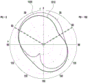
Fig. 9a shows the resonant frequency of the patch antenna of fig. 6e, and fig. 9b is a graph indicating the axial ratio of circular polarization in the patch antenna of fig. 6 e.
Fig. 10a and 10b show radiation patterns when the posture of the portable electronic device of fig. 3a is a vertical mode (or portrait mode), and fig. 10c and 10d show radiation patterns when the posture of the portable electronic device of fig. 3a is a horizontal mode (or landscape mode).
FIG. 11 illustrates the operation of a processor for positioning according to an embodiment.
Detailed Description
Fig. 1 is a block diagram illustrating an electronic device 101 in a network environment 100 according to various embodiments. Referring to fig. 1, an electronic device 101 in a network environment 100 may communicate with the electronic device 102 via a first network 198 (e.g., a short-range wireless communication network) or with at least one of the electronic device 104 or the server 108 via a second network 199 (e.g., a long-range wireless communication network). According to an embodiment, the electronic device 101 may communicate with the electronic device 104 via the server 108. According to an embodiment, the electronic device 101 may include a processor 120, a memory 130, an input module 150, a sound output module 155, a display module 160, an audio module 170, a sensor module 176, an interface 177, a connection end 178, a haptic module 179, a camera module 180, a power management module 188, a battery 189, a communication module 190, a Subscriber Identity Module (SIM) 196, or an antenna module 197. In some embodiments, at least one of the above-described components (e.g., connection end 178) may be omitted from electronic device 101, or one or more other components may be added to electronic device 101. In some embodiments, some of the components described above (e.g., sensor module 176, camera module 180, or antenna module 197) may be implemented as a single integrated component (e.g., display module 160).
The processor 120 may run, for example, software (e.g., program 140) to control at least one other component (e.g., hardware component or software component) of the electronic device 101 that is connected to the processor 120, and may perform various data processing or calculations. According to one embodiment, as at least part of the data processing or calculation, the processor 120 may store commands or data received from another component (e.g., the sensor module 176 or the communication module 190) into the volatile memory 132, process the commands or data stored in the volatile memory 132, and store the resulting data in the non-volatile memory 134. According to an embodiment, the processor 120 may include a main processor 121 (e.g., a Central Processing Unit (CPU) or an Application Processor (AP)) or an auxiliary processor 123 (e.g., a Graphics Processing Unit (GPU), a Neural Processing Unit (NPU), an Image Signal Processor (ISP), a sensor hub processor, or a Communication Processor (CP)) that is operatively independent of or combined with the main processor 121. For example, when the electronic device 101 comprises a main processor 121 and a secondary processor 123, the secondary processor 123 may be adapted to consume less power than the main processor 121 or to be dedicated to a particular function. The auxiliary processor 123 may be implemented separately from the main processor 121 or as part of the main processor 121.
The auxiliary processor 123 (instead of the main processor 121) may control at least some of the functions or states related to at least one of the components of the electronic device 101 (e.g., the display module 160, the sensor module 176, or the communication module 190) when the main processor 121 is in an inactive (e.g., sleep) state, or the auxiliary processor 123 may control at least some of the functions or states related to at least one of the components of the electronic device 101 (e.g., the display module 160, the sensor module 176, or the communication module 190) with the main processor 121 when the main processor 121 is in an active state (e.g., running an application). According to an embodiment, the auxiliary processor 123 (e.g., an image signal processor or a communication processor) may be implemented as part of another component (e.g., the camera module 180 or the communication module 190) functionally related to the auxiliary processor 123. According to an embodiment, the auxiliary processor 123 (e.g., a neural processing unit) may include hardware structures dedicated to artificial intelligence model processing. The artificial intelligence model may be generated through machine learning. Such learning may be performed, for example, by the electronic device 101 where artificial intelligence is performed or via a separate server (e.g., server 108). The learning algorithm may include, but is not limited to, for example, supervised learning, unsupervised learning, semi-supervised learning, or reinforcement learning. The artificial intelligence model may include a plurality of artificial neural network layers. The artificial neural network may be a Deep Neural Network (DNN), a Convolutional Neural Network (CNN), a Recurrent Neural Network (RNN), a boltzmann machine limited (RBM), a Deep Belief Network (DBN), a bi-directional recurrent deep neural network (BRDNN), or a deep Q network, or a combination of two or more thereof, but is not limited thereto. Additionally or alternatively, the artificial intelligence model may include software structures in addition to hardware structures.
The memory 130 may store various data used by at least one component of the electronic device 101 (e.g., the processor 120 or the sensor module 176). The various data may include, for example, software (e.g., program 140) and input data or output data for commands associated therewith. Memory 130 may include volatile memory 132 or nonvolatile memory 134.
The program 140 may be stored as software in the memory 130, and the program 140 may include, for example, an Operating System (OS) 142, middleware 144, or applications 146.
The input module 150 may receive commands or data from outside the electronic device 101 (e.g., a user) to be used by other components of the electronic device 101 (e.g., the processor 120). The input module 150 may include, for example, a microphone, a mouse, a keyboard, keys (e.g., buttons) or a digital pen (e.g., a stylus).
The sound output module 155 may output a sound signal to the outside of the electronic device 101. The sound output module 155 may include, for example, a speaker or a receiver. Speakers may be used for general purposes such as playing multimedia or playing a record. The receiver may be used to receive an incoming call. Depending on the embodiment, the receiver may be implemented separate from the speaker or as part of the speaker.
The audio module 170 may convert sound into electrical signals and vice versa. According to an embodiment, the audio module 170 may obtain sound via the input module 150, or output sound via the sound output module 155 or headphones of an external electronic device (e.g., the electronic device 102) that is directly (e.g., wired) or wirelessly connected to the electronic device 101.
The sensor module 176 may detect an operational state (e.g., power or temperature) of the electronic device 101 or an environmental state (e.g., a state of a user) external to the electronic device 101 and then generate an electrical signal or data value corresponding to the detected state. According to an embodiment, the sensor module 176 may include, for example, a gesture sensor, a gyroscope sensor, an atmospheric pressure sensor, a magnetic sensor, an acceleration sensor, a grip sensor, a proximity sensor, a color sensor, an Infrared (IR) sensor, a biometric sensor, a temperature sensor, a humidity sensor, or an illuminance sensor.
The connection end 178 may include a connector via which the electronic device 101 may be physically connected with an external electronic device (e.g., the electronic device 102). According to an embodiment, the connection end 178 may include, for example, an HDMI connector, a USB connector, an SD card connector, or an audio connector (e.g., a headphone connector).
The haptic module 179 may convert the electrical signal into a mechanical stimulus (e.g., vibration or motion) or an electrical stimulus that may be recognized by the user via his sense of touch or kinesthetic sense. According to an embodiment, the haptic module 179 may include, for example, a motor, a piezoelectric element, or an electrostimulator.
The camera module 180 may capture still images or moving images. According to an embodiment, the camera module 180 may include one or more lenses, an image sensor, an image signal processor, or a flash.
The power management module 188 may manage power supply to the electronic device 101. According to an embodiment, the power management module 188 may be implemented as at least part of, for example, a Power Management Integrated Circuit (PMIC).
The communication module 190 may support establishing a direct (e.g., wired) communication channel or a wireless communication channel between the electronic device 101 and an external electronic device (e.g., the electronic device 102, the electronic device 104, or the server 108) and performing communication via the established communication channel. The communication module 190 may include one or more communication processors capable of operating independently of the processor 120 (e.g., an Application Processor (AP)) and supporting direct (e.g., wired) or wireless communication. According to an embodiment, the communication module 190 may include a wireless communication module 192 (e.g., a cellular communication module, a short-range wireless communication module, or a Global Navigation Satellite System (GNSS) communication module) or a wired communication module 194 (e.g., a Local Area Network (LAN) communication module or a Power Line Communication (PLC) module). A respective one of these communication modules may communicate with external electronic devices via a first network 198 (e.g., a short-range communication network such as bluetooth, wireless fidelity (Wi-Fi) direct, or infrared data association (IrDA)) or a second network 199 (e.g., a long-range communication network such as a conventional cellular network, a 5G network, a next-generation communication network, the internet, or a computer network (e.g., a LAN or wide-area network (WAN)). These various types of communication modules may be implemented as a single component (e.g., a single chip), or may be implemented as multiple components (e.g., multiple chips) separate from each other. The wireless communication module 192 may identify and authenticate the electronic device 101 in a communication network, such as the first network 198 or the second network 199, using user information (e.g., an International Mobile Subscriber Identity (IMSI)) stored in the user identification module 196.
The wireless communication module 192 may support a 5G network following a 4G network as well as next generation communication technologies (e.g., new Radio (NR) access technologies). NR access technologies may support enhanced mobile broadband (eMBB), large-scale machine type communication (mctc), or Ultra Reliable Low Latency Communication (URLLC). The wireless communication module 192 may support a high frequency band (e.g., millimeter wave band) to achieve, for example, a high data transmission rate. The wireless communication module 192 may support various techniques for ensuring performance over high frequency bands, such as, for example, beamforming, massive multiple-input multiple-output (massive MIMO), full-dimensional MIMO (FD-MIMO), array antennas, analog beamforming, or massive antennas. The wireless communication module 192 may support various requirements specified in the electronic device 101, an external electronic device (e.g., electronic device 104), or a network system (e.g., second network 199). According to an embodiment, the wireless communication module 192 may support a peak data rate (e.g., 20Gbps or greater) for implementing an eMBB, a lost coverage (e.g., 164dB or less) for implementing an emtc, or a U-plane delay (e.g., a round trip of 0.5ms or less, or 1ms or less for each of the Downlink (DL) and Uplink (UL)) for implementing a URLLC.
The antenna module 197 may transmit signals or power to the outside of the electronic device 101 (e.g., an external electronic device) or receive signals or power from the outside of the electronic device 101 (e.g., an external electronic device). According to an embodiment, the antenna module 197 may include an antenna including a radiating element composed of a conductive material or conductive pattern formed in or on a substrate, such as a Printed Circuit Board (PCB). According to an embodiment, the antenna module 197 may include a plurality of antennas (e.g., array antennas). In this case, at least one antenna suitable for a communication scheme used in a communication network, such as the first network 198 or the second network 199, may be selected from the plurality of antennas, for example, by the communication module 190 (e.g., the wireless communication module 192). Signals or power may then be transmitted or received between the communication module 190 and the external electronic device via the selected at least one antenna. According to an embodiment, further components (e.g., a Radio Frequency Integrated Circuit (RFIC)) other than radiating elements may additionally be formed as part of the antenna module 197.
According to various embodiments, antenna module 197 may form a millimeter wave antenna module. According to embodiments, a millimeter-wave antenna module may include a printed circuit board, a Radio Frequency Integrated Circuit (RFIC) disposed on a first surface (e.g., a bottom surface) of the printed circuit board or adjacent to the first surface and capable of supporting a specified high frequency band (e.g., a millimeter-wave band), and a plurality of antennas (e.g., array antennas) disposed on a second surface (e.g., a top surface or a side surface) of the printed circuit board or adjacent to the second surface and capable of transmitting or receiving signals of the specified high frequency band.
At least some of the above components may be interconnected via an inter-peripheral communication scheme (e.g., bus, general Purpose Input Output (GPIO), serial Peripheral Interface (SPI), or Mobile Industrial Processor Interface (MIPI)) and communicatively communicate signals (e.g., commands or data) therebetween.
According to an embodiment, commands or data may be sent or received between the electronic device 101 and the external electronic device 104 via the server 108 connected to the second network 199. Each of the electronic device 102 or the electronic device 104 may be the same type of device as the electronic device 101 or a different type of device from the electronic device 101. According to an embodiment, all or some of the operations to be performed at the electronic device 101 may be performed at one or more of the external electronic device 102, the external electronic device 104, or the server 108. For example, if the electronic device 101 should automatically perform a function or service or should perform a function or service in response to a request from a user or another device, the electronic device 101 may request the one or more external electronic devices to perform at least part of the function or service instead of or in addition to the function or service, or the electronic device 101 may request the one or more external electronic devices to perform at least part of the function or service. The one or more external electronic devices that received the request may perform the requested at least part of the function or service or perform another function or another service related to the request and transmit the result of the performing to the electronic device 101. The electronic device 101 may provide the result as at least a partial reply to the request with or without further processing of the result. For this purpose, for example, cloud computing technology, distributed computing technology, mobile Edge Computing (MEC) technology, or client-server computing technology may be used. The electronic device 101 may provide ultra-low latency services using, for example, distributed computing or mobile edge computing. In another embodiment, the external electronic device 104 may comprise an internet of things (IoT) device. Server 108 may be an intelligent server using machine learning and/or neural networks. According to an embodiment, the external electronic device 104 or the server 108 may be included in the second network 199. The electronic device 101 may be applied to smart services (e.g., smart home, smart city, smart car, or healthcare) based on 5G communication technology or IoT-related technology.
The electronic device according to various embodiments may be one of various types of electronic devices. The electronic device may include, for example, a portable communication device (e.g., a smart phone), a computer device, a portable multimedia device, a portable medical device, a camera, a wearable device, or a household appliance. According to the embodiments of the present disclosure, the electronic device is not limited to those described above.
It should be understood that the various embodiments of the disclosure and the terminology used therein are not intended to limit the technical features set forth herein to the particular embodiments, but rather include various modifications, equivalents or alternatives to the respective embodiments. For the description of the drawings, like reference numerals may be used to refer to like or related elements. It will be understood that a noun in the singular corresponding to a term may include one or more things unless the context clearly indicates otherwise. As used herein, each of the phrases such as "a or B", "at least one of a and B", "at least one of a or B", "A, B or C", "at least one of A, B and C", and "at least one of A, B or C" may include any or all possible combinations of items listed with a corresponding one of the plurality of phrases. As used herein, terms such as "1 st" and "2 nd" or "first" and "second" may be used to simply distinguish one element from another element and not to limit the element in other respects (e.g., importance or order). It will be understood that if the terms "operatively" or "communicatively" are used or the terms "operatively" or "communicatively" are not used, then if an element (e.g., a first element) is referred to as being "coupled to," "connected to," or "connected to" another element (e.g., a second element), it is intended that the element can be directly (e.g., wired) connected to, wireless connected to, or connected to the other element via a third element.
As used in connection with various embodiments of the present disclosure, the term "module" may include an element implemented in hardware, software, or firmware, and may be used interchangeably with other terms (e.g., "logic," "logic block," "portion," or "circuitry"). A module may be a single integrated component adapted to perform one or more functions or a minimal unit or portion of the single integrated component. For example, according to an embodiment, a module may be implemented in the form of an Application Specific Integrated Circuit (ASIC).
The various embodiments set forth herein may be implemented as software (e.g., program 140) comprising one or more instructions stored in a storage medium (e.g., internal memory 136 or external memory 138) readable by a machine (e.g., electronic device 101). For example, under control of a processor, a processor (e.g., processor 120) of the machine (e.g., electronic device 101) may invoke and execute at least one of the one or more instructions stored in the storage medium with or without the use of one or more other components. This enables the machine to operate to perform at least one function in accordance with the at least one instruction invoked. The one or more instructions may include code generated by a compiler or code capable of being executed by an interpreter. The machine-readable storage medium may be provided in the form of a non-transitory storage medium. Wherein the term "non-transitory" merely means that the storage medium is a tangible device and does not include a signal (e.g., electromagnetic waves), but the term does not distinguish between data being semi-permanently stored in the storage medium and data being temporarily stored in the storage medium.
According to embodiments, methods according to various embodiments of the present disclosure may be included and provided in a computer program product. The computer program product may be used as a product for conducting transactions between sellers and buyers. The computer program product may be distributed in the form of a machine-readable storage medium, such as a compact disk read only memory (CD-ROM), or may be distributed (e.g., downloaded or uploaded) online via an application store, such as a playstore (tm), or may be distributed (e.g., downloaded or uploaded) directly between two user devices, such as smartphones. At least some of the computer program product may be temporarily generated if published online, or at least some of the computer program product may be stored at least temporarily in a machine readable storage medium, such as the memory of a manufacturer's server, an application store's server, or a forwarding server.
According to various embodiments, each of the above-described components (e.g., a module or a program) may include a single entity or multiple entities, and some of the multiple entities may be separately provided in different components. According to various embodiments, one or more of the above components may be omitted, or one or more other components may be added. Alternatively or additionally, multiple components (e.g., modules or programs) may be integrated into a single component. In this case, according to various embodiments, the integrated component may still perform the one or more functions of each of the plurality of components in the same or similar manner as the corresponding one of the plurality of components performed the one or more functions prior to integration. According to various embodiments, operations performed by a module, a program, or another component may be performed sequentially, in parallel, repeatedly, or in a heuristic manner, or one or more of the operations may be performed in a different order or omitted, or one or more other operations may be added.
Fig. 2 is a block diagram 200 illustrating a wireless communication module 192 and an antenna module 197 of the electronic device 101 in accordance with various embodiments. Referring to fig. 2, the wireless communication module 192 may include a bluetooth communication circuit 210 and/or a UWB communication circuit 220. Antenna module 197 may include a bluetooth antenna 250 connected to bluetooth communication circuitry 210 and/or a UWB antenna 260 connected to UWB communication circuitry 220. At least one function of the bluetooth communication circuit 210 and the UWB communication circuit 220 may be controlled by the processor 120 (e.g., an application processor and/or a communication processor).
The UWB communication circuit 220 may support establishment of UWB communication channels (or sessions) corresponding to frequency bands (e.g., about 3.1 to 10.6 GHz) designated for UWB communication among frequency bands for wireless communication with external electronic devices (e.g., the external electronic device 102 of fig. 1). UWB communication circuitry 220 may support UWB communications with external electronic devices over a UWB communication channel. During transmission, UWB communication circuit 220 may convert baseband signals generated by processor 120 (e.g., an application processor and/or a communication processor) and received from processor 120 into RF signals of the UWB band to be transmitted to the outside through UWB antenna 260. During reception, the UWB communication circuit 220 may acquire an RF signal of a UWB band through the UWB antenna 260 and convert the acquired RF signal into a baseband signal to transmit the converted signal to the processor 120. Although not shown, the wireless communication module 192 may also include a filter (e.g., UWB band pass filter) for filtering out RF signals of the UWB band from RF signals received from the UWB antenna 260 and transmitting them to the UWB communication circuit 220. Although not shown, UWB antenna 260 may include a plurality of antennas. For example, UWB antenna 260 may include an RF signal transmitting or receiving first antenna or an RF signal receiving second antenna and/or a third antenna.
According to various embodiments, bluetooth may be used as a trigger for activating UWB communications. For example, BLE has relatively low positioning accuracy compared to other short-range communication technologies (e.g., UWB technology), but has low power consumption and long identification distance (e.g., distance that can identify the presence of surrounding external electronic devices 102), and thus BLE can be used to trigger activation of positioning communications. In an embodiment, the processor 120 may receive a signal (e.g., an advertisement or a broadcast packet) from the external electronic device 102 for connection with the external electronic device 102 through the bluetooth communication circuit 210. For example, the external electronic device 102 may send a signal as an advertiser (or broadcaster), and the electronic device 101 may periodically scan the signal as an observer. When the strength of the received signal (e.g., RSSI) has a value greater than a specified threshold or the strength of the signal is identified as becoming stronger, the processor 120 may determine to activate positioning communications employing UWB. Based on this determination, the processor 120 may establish a UWB communication channel (e.g., a second frequency band (e.g., ch5, about 6.5GHz, or about 6.25 to 6.75 GHz) or a first frequency (e.g., ch9, about 8GHz band, or about 7.75 to 8.25 GHz)) with the external electronic device 102 by using the UWB communication circuit 220. For example, when the UWB communication circuit 220 is in a disabled state (e.g., a sleep state or a power-off state), the processor 120 may transition the state of the UWB communication circuit 220 to an enabled state based on the determination and perform positioning communication with the external electronic device 101 through the established UWB communication channel. In another embodiment, the processor 120 may establish a BLE communication channel with the external electronic device 102 by using the bluetooth communication circuit 210. The processor 120 may determine to activate positioning communications employing UWB based on the strength of a signal received from the external electronic device 102 over the established BLE communication channel (e.g., when the strength has a value greater than a specified threshold or the strength of the signal becomes stronger). Based on this determination, the processor 120 can establish a UWB communication channel with the external electronic device 102 by using the UWB communication circuit 220, and perform positioning communication with the external electronic device 101 through the established UWB communication channel. Communication technologies other than bluetooth (e.g., wi-Fi) may also be used as a trigger for activating positioning communications.
Fig. 3a and 3b illustrate an arrangement of UWB antennas in a portable electronic device 300 (e.g., electronic device 101 of fig. 1) having a bar-shaped housing structure according to an embodiment. The surface of the portable electronic device 300 where the display (e.g., the display module 160 of fig. 1) is located may be defined as a front surface, a surface opposite to the front surface may be defined as a rear surface of the portable electronic device 300, and a surface surrounding a space between the front surface and the rear surface may be defined as a side surface of the portable electronic device 300. Fig. 3a is a view of the portable electronic device 300 showing the rear cover removed, and fig. 3b shows the portable electronic device 300 to which the rear cover is coupled. Referring to fig. 3a and 3b, a portable electronic device 300 (e.g., the electronic device 101 of fig. 1) may include a housing 310, a camera cover 320, a UWB antenna 330, and/or a support member 340.
According to an embodiment, the housing 310 may include a front cover (not shown), a rear cover 311, and/or a side frame 312.UWB antenna 330 and support member 340 may be disposed inside housing 310. In an embodiment, the camera cover 320 may decorate a camera module (e.g., the camera module 180) disposed inside the housing 310 as a cover of the camera module, and may be implemented as a metal or a polymer.
According to an embodiment, UWB antenna 330 (e.g., UWB antenna 260 of fig. 2) may be disposed inside housing 310 while not overlapping the camera module when facing the rear surface. The UWB antenna 330 may be electrically disconnected from the camera cover 320 and may be disposed between the rear cover 311 and the support member 340.
According to an embodiment, the support member 340 may be disposed between the UWB antenna 330 and a substrate (e.g., a Printed Circuit Board (PCB)) (not shown). For example, UWB antenna 330 may be disposed on support member 340. The support member 340 may be implemented as, for example, a metal (e.g., SUS) or a polymer. In an embodiment, the support member 340 may be formed as a hole 350 to be fixed inside the case 310 by using a fixing member (e.g., a screw). For example, the support member 340 may be electrically connected to the side frame 312 (e.g., a metal body) by a screw. For example, UWB antenna 330 may be electrically connected to a UWB communication circuit (e.g., UWB communication circuit 220 of fig. 2) through a signal line formed on the substrate.
According to an embodiment, a portable electronic device (e.g., electronic device 101 of fig. 1) may have a foldable housing that is divided into two housings with reference to a folding axis. A first portion of a display (e.g., a flexible display) may be disposed on the first housing and a second portion of the display may be disposed on the second housing. The foldable housing may be implemented as an internal folding scheme in which the first and second portions face each other when the portable electronic device is folded. Alternatively, the foldable housing may be implemented as an external folding scheme, wherein the first and second portions are oriented opposite to each other when the portable electronic device is folded. The surface on which the first and second portions of the display are disposed may be defined as a front surface of the portable electronic device, a surface opposite to the front surface may be defined as a rear surface of the portable electronic device, and a surface surrounding a space between the front surface and the rear surface may be defined as a side surface of the portable electronic device.
Fig. 4a and 4b show an arrangement of UWB antennas in a portable electronic device 400 with an inner folding scheme foldable housing structure according to an embodiment. Referring to fig. 4a and 4b, the portable electronic device 400 may include foldable housings 410 and 420, a camera cover 430, a UWB antenna 440, and/or a support member 450. The foldable housing may include a first housing 410 and a second housing 420. The first case 410 may include a first rear cover (not shown) forming a portion of the rear surface of the portable electronic device 400. The second case 420 may include a second rear cover 421 forming another part of the rear surface of the portable electronic device 400. In an embodiment, the UWB antenna 440 and/or the support member 450 may be disposed inside the first housing 410. In an embodiment, the camera cover 430 may decorate the camera module as a cover of the camera module received inside the first case 410, and may be implemented as metal or polymer.
According to an embodiment, a UWB antenna 440 (e.g., UWB antenna 260 of fig. 2) may be disposed inside the first case 410 while not overlapping with a camera module (e.g., camera module 180 of fig. 1) when facing the rear surface. The UWB antenna 440 may be electrically disconnected from the camera cover 430 and may be disposed between the first rear cover and the support member 450.
According to an embodiment, the support member 450 may be disposed between the UWB antenna 440 and a substrate (e.g., PCB) (not shown) disposed inside the first case 410. The support member may be coupled to the UWB antenna 440 and may be implemented as injection molding. The UWB antenna 440 may be electrically connected to a UWB communication circuit (e.g., UWB communication circuit 220 of fig. 2) through a signal line formed on the substrate.
According to an embodiment, an antenna other than UWB antenna 440 (e.g., antenna 460 for NFC and/or MST) may be disposed inside first housing 410. In an embodiment, the portable electronic device 400 may further include a second display disposed inside the second housing 470 and exposed through the second rear cover 421, in addition to the first display exposed through the front surface.
Fig. 5 illustrates a side surface of a UWB antenna 500 having a laminated structure according to various embodiments. Referring to fig. 5, a UWB antenna 500 (e.g., UWB antenna 260 of fig. 2) may be implemented as a two-layer structure FPCB including a first conductive layer (or top conductive layer) 510 and a second conductive layer (e.g., bottom conductive layer) 520. The first conductive layer 510 may be formed on one surface of the dielectric substrate (or dielectric layer) 530, and the second conductive layer 520 may be formed on the other surface of the dielectric substrate 530.
According to an embodiment, the first conductive layer 510 may include patch antennas and a transmission line (or feed line) for connecting each patch antenna to a UWB communication circuit (e.g., UWB communication circuit 220 of fig. 2). The second conductive layer 520 may form a common ground for the patch antenna. The patch antenna and the ground may operate as a resonator for transmitting RF signals of a specific frequency band (e.g., a second frequency band (e.g., ch5 or about 6.5GHz band) or a first frequency band (e.g., ch9 or about 8GHz band)) to the outside and receiving RF signals of the specific frequency band. In an embodiment, the first conductive layer 510 may include a first copper layer 511 and/or a first plating (e.g., copper plating) 512 plated with the first copper layer. In an embodiment, the second conductive layer 520 may include a second copper layer 521 and a second plating layer (e.g., copper plating) 522 plated with the second copper layer. As another example, an insulating material such as a polymer may be disposed on the first conductive layer 510 or the second conductive layer 520.
According to an embodiment, the dielectric substrate 530 may be implemented such that the UWB antenna 500 transmits or receives RF signals of a specific frequency band. For example, the dielectric substrate 530 may include a first Modified Polyimide (MPI) 531, a second MPI 532, a third MPI 533, a first bonding pad 534, and/or a second bonding pad 535. The first copper layer 511 and the first MPI 531 are main materials of the FPCB, and a first Flexible Copper Clad Laminate (FCCL) 501 may be formed. The second copper layer 521 and the second MPI 532 may form a second FCCL 502. The first bonding pad 534 may be disposed between the first MPI 531 and the third MPI 533 to bond the first MPI 531 and the third MPI 533. The second engagement tab 535 may be disposed between the second MPI 532 and the third MPI 533 to engage the second MPI 532 and the third MPI 533. The third MPI 533 may be disposed between the first bonding pad 534 and the second bonding pad 535. The radiation efficiency may be considered when determining the thickness of the dielectric substrate 530. For example, as the thickness of the dielectric substrate 530 decreases, the radiation efficiency in a specific frequency band may decrease. In an embodiment, the third MPI 533 may be added to the dielectric substrate 530 as a supplementary material for supplementing the thickness of the dielectric substrate 530. In another example, when the supplemental thickness is not required, the third MPI 533 and at least one of the first bonding pad 534 and the second bonding pad 535 may be omitted from the elements of the dielectric substrate 530.
Fig. 6a shows a surface of a first conductive layer 601 of the UWB antenna according to an embodiment, fig. 6b shows a surface of a second conductive layer 602 disposed under the first conductive layer 601, and fig. 6c is a perspective view showing the UWB antenna on which the first conductive layer 601 and the second conductive layer 602 are disposed. Fig. 6d, 6e and 6f illustrate various embodiments of patch antennas included in UWB antennas. Fig. 6g and 6h show the position of the feed point for each patch antenna of the first conductive layer 601.
Referring to fig. 6a, a first conductive layer 601 (e.g., first conductive layer 510 of fig. 5) may include a first patch antenna 610, a second patch antenna 620, a third patch antenna 630, a first transmission line 641, a second transmission line 642, and/or a third transmission line 643. In an embodiment, one of the patch antennas 610, 620, and 630 (e.g., the first patch antenna 610) may be used as an antenna for UWB signal transmission or reception, and the other two may be used as antennas for UWB signal reception.
According to an embodiment, the first patch antenna 610 and the second patch antenna 620 may be aligned in a first direction (y-axis direction) while not overlapping each other when viewed facing the rear surface (XY plane), so that an angle (e.g., an elevation angle of the AoA) in the y-axis direction may be measured. For example, the second patch antenna 620 may be disposed to be spaced apart from the first patch antenna 610 in the first direction while not overlapping the first patch antenna. The second patch antenna 620 may have substantially the same shape and size as the first patch antenna 610. The center of the first patch antenna 610 may be spaced apart from the center of the second patch antenna 620 by a space (dx) in the x-axis direction. The center of the second patch antenna 620 may be spaced apart from the center of the first patch antenna in the y-axis direction by a space (W1).
According to an embodiment, the first patch antenna 610 and the third patch antenna 630 may be aligned in a second direction (x-axis direction) substantially perpendicular to the first direction while not overlapping each other when viewed facing the rear surface (XY plane), so that an angle (e.g., azimuth angle of AoA) in the x-axis direction may be measured. For example, the third patch antenna 630 may be disposed to be spaced apart from the first patch antenna 610 in the third direction (-x-axis direction) while not overlapping the first patch antenna. The third patch antenna 630 may have substantially the same shape and size as the first patch antenna 610. The center of the third patch antenna 630 may be spaced apart from the center of the first patch antenna 610 in the y-axis direction by a space (dy). The center of the third patch antenna 630 may be spaced apart from the center of the first patch antenna 610 in the x-axis direction by a space (W2).
According to an embodiment, the interval (W1), the interval (W2), the interval (dx), or the interval (dy) may be determined based on a resonance frequency band of the UWB antenna, and may be determined not to exceed a half wavelength in consideration of characteristics of the AoA. For example, when the resonance frequency bands of the UWB antenna are ch5 and ch9, the interval (W1) may be implemented to be about 13 to 20mm (e.g., about 14 mm), and the interval (dx) may be implemented to be about 3.6mm. The spacing (W2) may be implemented to be about 13 to 20mm (e.g., about 13 mm), and the spacing (dy) may be implemented to be about 1.0mm
According to an embodiment, a plurality of slits may be formed at the patch antennas 610, 620, and 630 to perform simultaneous resonance in dual frequency bands, and transmit and/or receive vertical linear polarization in which a polarity direction of an electric field is a y-axis direction and a traveling direction of an RF signal is a z-axis direction, and horizontal linear polarization in which a polarity direction of an electric field is an x-axis direction and a traveling direction of an RF signal is a z-axis direction. According to an embodiment, patch antennas 610, 620, and 630 may be symmetrical when viewed with reference to the x-axis direction and the y-axis direction. For example, each of the patch antennas 610, 620, and 630 may be rectangular (or square) in shape. The first patch antenna 610 may include a first side (or left side) 611 extending in the y-axis direction, a second side (or right side) 612 parallel to the first side 611, a third side (or top side) 613 extending in the x-axis direction, and a fourth side (or bottom side) 614 parallel to the third side. The first slit 611a may be formed in a straight line from the center of the first side 611 toward the second side 612 so as to be perpendicular to the first side 611. The second slit 612a may be formed in a straight line from the center of the second side 612 toward the first side 611 so as to be perpendicular to the second side 612. The third slit 613a may be formed in a straight line from the center of the third side 613 toward the fourth side 614 so as to be perpendicular to the third side 613. The fourth slit 614a may be formed in a straight line from the center of the fourth side 614 toward the third side 613 so as to be perpendicular to the fourth side 614. The vertical line polarization of the first frequency band may be transmitted or received by the lengths of the electric emission current of the first side 611, the first slit 611a formed on the first side 611, the second side 612, and the second slit 612a formed on the second side 612. The horizontal linear polarization of the second frequency band may be transmitted or received by the lengths of the third side 613, the third slit 613a formed on the third side 613, the fourth side 614, and the fourth slit 614a formed on the fourth side 614. In an embodiment, a slit having substantially the same shape as the slit of the first patch antenna 610 may also be formed at each of the second patch antenna 620 and the third patch antenna 630. For example, a slit may be formed at substantially the same position as the first patch antenna 610.
According to an embodiment, the lengths of the sides and slits of the first patch antenna 610, the second patch antenna 620, or the third patch antenna 630 may be implemented according to a resonance frequency band. For example, in fig. 6a, the lengths of the first side 611, the second side 612, the first slit 611a, and the second slit 612a of the first patch antenna 610 may be implemented according to a first frequency band (e.g., ch9 or about 8GHz band), and the lengths of the third side 613, the fourth side 614, the third slit 613a, and the fourth slit 614a may be implemented according to a second frequency band (e.g., ch5 or about 6.5GHz band). Fig. 6d shows that the lengths of the first side 671, the second side 672, the first slit 671a and the second slit 672a are implemented according to a second frequency band (e.g., ch5 or about 6.5GHz band), and the lengths of the third side 673, the fourth side 674, the third slit 673a and the fourth slit 674a are implemented according to a first frequency band (e.g., ch9 or about 8GHz band).
According to the embodiment, when the antenna for transmitting the RF signal has the same polarity direction as the antenna for receiving the RF signal, the reception efficiency of the receiving antenna can be improved. When the polarity directions of the transmitting antenna and the receiving antenna are different, the receiving efficiency of the receiving antenna may be lowered. In another example, a patch antenna implemented to receive circular polarization may have relatively low reception efficiency compared to a patch antenna implemented to receive linear polarization, but when the antenna receives not only circular polarization but also vertical linear polarization and horizontal linear polarization, the reception efficiency of a patch antenna implemented to receive circular polarization may be improved compared to a patch antenna implemented to receive linear polarization. In another example, a patch antenna implemented to receive linear polarization has lower reception efficiency than a case of receiving linear polarization having the same polarity direction, but when the patch antenna receives circular polarization, the reception efficiency may be improved compared to a case of receiving linear polarization having different polarity directions.
According to an embodiment, the patch antenna may be implemented such that resonance is performed in a single frequency band and circular polarization is transmitted (or received). For example, referring to fig. 6e, the patch antenna 680 may have the same overall shape as the first patch antenna 610, and may have a structure in which triangles of an upper right corner and a lower left corner are cut out with reference to the currently illustrated drawing, thereby transmitting or receiving right circular polarization (RHCP). The shape of the slit 681 formed at the patch antenna 680 may be formed based on the frequency supported by the patch antenna 680, for example, a first frequency band (e.g., ch9 or about 8GHz band). Referring to fig. 6f, the patch antenna 690 may have the same overall shape as the first patch antenna 610, and may have a structure in which triangles of a lower right corner and an upper left corner are cut out with reference to the currently illustrated drawing, thereby transmitting or receiving left-hand circular polarization (LHCP). The shape of the slit 691 formed at the patch antenna 690 may be formed based on the frequency supported by the patch antenna 690 (e.g., a first frequency band (e.g., ch9 or about 8GHz band)).
Referring to fig. 6b, a second conductive layer 602 (e.g., second conductive layer 320 of fig. 3) according to an embodiment may include a ground pattern 603. Referring to fig. 6b and 6c, a ground pattern 603 may be disposed on a substrate (e.g., the dielectric substrate 530 of fig. 5) to overlap the first conductive layer 601 when viewed facing the rear surface (XY plane). For example, patch antennas 610, 620, and 630 or transmission lines 641, 642, and 643 included in the first conductive layer 601 may overlap with the ground pattern 603 when viewed in the +z-axis direction. In another example, patch antennas 610, 620, and 630 or transmission lines 641, 642, and 643 included in the first conductive layer 601, which are disposed to overlap with the ground pattern 603, may be hidden by the ground pattern 603 when viewed from the-z axis direction. In another example, the area of the ground pattern 603 may be larger than the area of the patch antennas 610, 620, and 630 or the transmission lines 641, 642, and 643.
According to an embodiment, the ground pattern 603 may be formed of one metal plate as a common ground of the patch antennas 610, 620, and 630, and thus may have a relatively rigid property. Such rigidity may cause a contact failure between the substrate and the connector 650, for example, when the electronic device is subjected to an impact from the outside. For example, the substrate may have UWB communication circuitry disposed thereon, or may be electrically connected to UWB communication circuitry. In an embodiment, in order to maintain contact with the substrate, a portion of the ground pattern 603 that overlaps the connector 650 when viewed in the +z-axis direction may be flexibly implemented. For example, the portion of the ground pattern 603 overlapping the connector 650 may have a conductive material composition ratio different from that of the portion of the non-overlapping connector 650. In an embodiment, the slit 631 may be formed not to overlap the transmission lines 641, 642, and 643 when viewed in the z-axis direction. In an embodiment, the slit 632 may be formed along the y-axis direction so as to be located between the first transmission line 641 and the first patch antenna 610 and not to overlap the first transmission line 641 and the first patch antenna 610 when viewed from the z-axis direction. In an embodiment, the slit 633 may be formed along the y-axis direction so as to be located between the third transmission line 643 and the third patch antenna 630 and not to overlap with the third transmission line 643 and the third patch antenna 630 when viewed from the z-axis direction.
According to an embodiment, a slit for uniformity of a radiation pattern (or beam pattern) may be formed on the ground pattern 603. Uniformity may be defined as a technical feature that causes the left and right radiation patterns to have symmetry with respect to a specified direction (e.g., the y-axis direction). For example, when viewed from the z-axis direction, the slit 634 may be formed at an edge of the ground pattern 603 in the x-axis direction so as to be located between the first patch antenna 610 and the second patch antenna 620 and not to overlap the first patch antenna 610 and the second patch antenna 620.
According to an embodiment, the positions of the feed points of the patch antennas 610, 620, and 630 connected to the transmission line are corners (or vertices) of the respective patch antennas. Referring to fig. 6a, all patch antennas 610, 620, and 630 may have substantially the same feed point in the upper left corner with reference to the presently illustrated drawing. In another example, the feed point may be located at a corner of the four corners of the patch antenna that causes the shortest signal path to be formed between the connector 650 and the patch antenna.
According to an embodiment, the length of the transmission line may vary as the position of the feed point varies. For example, referring to fig. 6g, when the upper right corner of the third patch antenna 630 is a feed point in a state where the slit 633 is formed between the third patch antenna 630 and the connector 650, a third transmission line 663 shorter than the third transmission line 643 of fig. 6c may be formed on the first conductive layer 601. In another example, when the ground pattern 603 is implemented without the slit 633 and the lower right corner of the third patch antenna 630 is a feed point, a third transmission line (not shown) shorter than the third transmission line 663 of fig. 6g may be formed on the first conductive layer 601. Referring to fig. 6h, when the lower left corner of the first patch antenna 610 is a feed point, a second transmission line 662 shorter than the second transmission line 642 of fig. 6c may be formed on the first conductive layer 601. The shorter the length of the transmission line, the smaller the loss of the UWB signal in the transmission line can become, and therefore, the radiation efficiency of the patch antenna can be improved. According to an embodiment, the first conductive layer 601 may be selectively implemented by a change in the length of the transmission line, and the AoA calculation may be applied by calibrating the phase difference according to the change in the length of the transmission line.
According to an embodiment, the transmission lines 641, 642, and 643 may extend from the connector 650 to the corner of each patch antenna by passing between the first patch antenna 610 and the third patch antenna 630 while not overlapping each other when viewed facing the rear surface (XY plane). The transmission lines 641, 642, and 643 may include first portions 641a, 642a, and 643a each having a first width (W3) and second portions 641b, 642b, and 643b each having a second width (W4). In an embodiment, the first width (W3) may be implemented such that the first portions 641a, 642a, and 643a have a characteristic impedance of, for example, 50 ohms. For example, the width of each of the first portions 641a, 642a, and 643a may be implemented to be about 0.5mm. In an embodiment, the second portions 641b, 642b, and 643b may serve as transformers (or transformers) for impedance conversion for matching the impedance of each of the patch antennas 610, 620, and 630 and the characteristic impedance of each of the first portions 641a, 642a, and 643 a. For example, the second width (W4) may be implemented to be narrower (e.g., about 0.15 mm) than the first width (W3), and the length of each of the second portions 641b, 642b, and 643b may be implemented to be about 5mm, for example. In another example, the width (e.g., second width (W4)) and length of each of the second portions 641b, 642b, and 643b may be adjusted for impedance matching between the corresponding patch antenna and the first portions 641a, 642a, 643 a. According to an embodiment, connector 650 may be electrically connected to UWB communication circuitry. For example, connector 650 may be electrically connected to UWB communication circuitry disposed on a substrate that is electrically connected to connector 650.
Fig. 7a, 7b and 7c illustrate a first conductive layer and a second conductive layer of a UWB antenna according to various embodiments.
Referring to fig. 7a, patch antennas 711, 712, and 713 (e.g., patch antennas 610, 620, and 630 of fig. 6 a) may be arranged in an inverted L shape on a first conductive layer (e.g., first conductive layer 510 of fig. 5), as shown in fig. 7 a. For example, the second patch antenna 712 may be disposed in the y-axis direction of the first patch antenna 711, and the third patch antenna 713 may be disposed in the-x-axis direction of the first patch antenna 711. The center of the first patch antenna 711 and the center of the second patch antenna 712 may be aligned in a row along the y-axis without misalignment (dx=0). The center of the first patch antenna 711 and the center of the third patch antenna 713 may be aligned in a row along the x-axis without misalignment (dy=0).
The connector 714 may be disposed in the-y axis direction of the first patch antenna 711 and the third patch antenna 713.
In an embodiment, the second conductive layer may be located below the first conductive layer in the-z-axis direction. The second conductive layer (e.g., second conductive layer 520 of fig. 5) may include a common ground pattern 702 (e.g., ground pattern 603 of fig. 6 b) for patch antennas 711, 712, and 713. The ground pattern 702 may be disposed to overlap with the patch antennas 711, 712, and 713 and the transmission lines 715, 716, and 717 when viewed in the z-axis direction. For example, when viewed from the z-axis direction, there are no portions of the patch antennas 711, 712, and 713 and the transmission lines 715, 716, and 717 that fall outside the ground pattern 702.
The slit 721 may be formed at an edge of the ground pattern 702 between the first transmission line 715 and the first patch antenna 711 in an extending direction (y-axis direction) of the first transmission line 715.
The slit 722 may be formed at an edge of the ground pattern 702 between the third transmission line 717 and the third patch antenna 713 in the extending direction (y-axis direction) of the third transmission line 717.
A slit 723 may be formed at an edge of the ground pattern 702 between the first patch antenna 711 and the second patch antenna 712 in the x-axis direction.
Referring to fig. 7b, referring to the currently illustrated drawing, the second transmission line 726 may extend from the connector 714 to the lower right corner of the second patch antenna 712 by passing between the first patch antenna 711 and the third patch antenna 713. Thus, the second transmission line 726 may be shortened compared to the second transmission line 716 of fig. 7 a. The portion 731 of the transmission line 716 that passes in the ground pattern 702 in fig. 7a may be removed from the ground pattern 702 by the shortened length of the transmission line. Referring to the currently illustrated drawing, the third transmission line 727 may extend from the connector 714 to the upper right corner of the third patch antenna 713 by passing between the first and third patch antennas 711 and 713. Therefore, the third transmission line 727 can be shortened as compared to the third transmission line 717 of fig. 7 a. The portion 732 of the third transmission line 717 of fig. 7a, which passes in the second conductive layer 702, can be removed from the ground pattern 702 by the shortened length of the transmission line.
Referring to fig. 7c, the ground pattern 702 may be formed to be physically separated into a first metal plate 751, a second metal plate 752, and a third metal plate 753. When facing the ground pattern 702, the first metal plate 751 may be disposed to overlap the first patch antenna 711 and the first transmission line 715, the second metal plate 752 may be disposed to overlap the second patch antenna 712 and the second transmission line 726, and the third metal plate 753 may be disposed to overlap the third patch antenna 713 and the third transmission line 727.
Fig. 8a shows horizontal linear polarization in the patch antenna according to an embodiment, fig. 8b shows vertical linear polarization in the patch antenna of fig. 8a, and fig. 8c shows dual resonance characteristics in the patch antenna of fig. 8 a.
Referring to fig. 8a, in a patch antenna 800 (e.g., the first patch antenna 610 of fig. 6 a), the resonant frequency may be determined by a horizontal length 810 and a vertical length 820. Dual resonance may be achieved in patch antenna 800 by a slot located at the edge. For example, as described above with reference to fig. 6a, a first slit 811a may be formed at the first side 811, and a second slit 812a may be formed at the second side 812, such that the patch antenna 800 resonates in a first frequency band (e.g., ch9 or about 8GHz band). A third slot 813a may be formed at the third side 813 and a fourth slot 814a may be formed at the fourth side 814 such that the patch antenna 800 resonates in a second frequency band (e.g., ch5 or about 6.5GHz band).
Referring to fig. 8a and 8c, the third slit 813a and the fourth slit 814a formed in the vertical direction may form a surface current path 830 corresponding to the second frequency band. Because of the formation of such surface current paths 830, patch antenna 800 may transmit and/or receive horizontal linear polarization of the second frequency band, where the polarity direction 840 of the electric field is a horizontal direction (x-axis direction) and the direction of travel is a z-axis direction.
Referring to fig. 8b and 8c, the first slit 811a and the second slit 812a formed in the horizontal direction may form a surface current path 850 corresponding to the first frequency band. Because of the formation of such surface current paths 850, patch antenna 800 may transmit and/or receive a vertical linear polarization of a first frequency band, where the polarity direction 860 of the electric field is a vertical direction (y-axis direction) and the direction of travel is a z-axis direction.
According to an embodiment, the lengths of the first slit 811a and the second slit 812a may be implemented to polarize a vertical line of the second frequency band (e.g., ch5 or about 6.5GHz band) transmitted and/or received by the patch antenna 800, and the lengths of the third slit 813a and the fourth slit 814a may be implemented to polarize a horizontal line of the first frequency band (e.g., ch9 or about 8GHz band) transmitted and/or received by the patch antenna 800. For example, the lengths of the first slit 811a and the second slit 812a may be shorter than those shown in fig. 8a, and the lengths of the third slit 813a and the fourth slit 814a may be longer than those shown in fig. 8 a.
Fig. 9a shows the resonant frequency of the patch antenna 680 of fig. 6e, and fig. 9b is a graph indicating the axial ratio of circular polarization in the patch antenna 680 of fig. 6 e. Referring to fig. 9a, patch antenna 680 may be implemented to resonate in a first frequency band (e.g., ch9 or about 8GHz band), for example. The axial ratio may mean a ratio of the polarity of an electric field in the x-axis direction to the polarity of an electric field in the y-axis direction. Referring to fig. 9b, it can be recognized that the polarization (e.g., the polarization closest to a circle) having the smallest axial ratio in the first frequency band in which the center frequency is about 8GHz appears in the patch antenna 680.
In an embodiment, the length of the slit 681 is implemented differently, and thus the resonant frequency of the patch antenna 680 may be, for example, the second frequency band.
Fig. 10a and 10b show radiation patterns when the posture of the portable electronic device 300 of fig. 3a is a vertical mode (or portrait mode), and fig. 10c and 10d show radiation patterns when the posture of the portable electronic device 300 of fig. 3a is a horizontal mode (or landscape mode).
Referring to fig. 10a and 10b, when a relatively shorter side of the two pairs of sides is placed parallel to the x-axis in the portable electronic device 300, the first patch antenna 610 and the third patch antenna 630 may be aligned in a direction substantially parallel to the x-axis, and the first patch antenna 610 and the second patch antenna 620 may be aligned in a direction substantially parallel to the y-axis. Accordingly, when the posture of the portable electronic device 300 is the portrait mode, the first patch antenna 610 and the third patch antenna 630 may be used to measure an angle (azimuth) of a UWB signal received in the UWB antenna in the x-axis direction. The first patch antenna 610 and the second patch antenna 620 may be used to measure an angle (elevation angle) of a UWB signal received in the UWB antenna in a y-axis direction. For example, a processor (e.g., processor 120 of fig. 1) may calculate a phase difference between the two signals by using a difference between a reception time of a first signal received from a first patch antenna 610 and a reception time of a second signal received from a second antenna 620, and calculate an elevation angle by using the phase difference and a distance (e.g., "interval (W1)" of fig. 6 a) between the two patch antennas 610 and 620. The processor may calculate a phase difference between the two signals by using a difference between the reception time of the first signal and the reception time of the third signal received from the third antenna 630, and calculate an azimuth angle by using the phase difference and a distance (e.g., "interval (W2)" of fig. 6 a) between the two patch antennas 610 and 630.
According to an embodiment, in order to install the UWB antenna in a limited space inside the portable electronic device 300, the common ground pattern of the patch antennas 610, 620, and 630 may be implemented to have an asymmetric structure instead of a structure (e.g., square) in which the right and left sides and/or the top and bottom sides are symmetrical to each other. Thus, the UWB signal of the UWB antenna may be transmitted in an asymmetric shape 1010 when viewed in the z-axis direction on the XY plane. Furthermore, although not shown in fig. 10b, an empty pattern in which no UWB signal is transmitted may be generated at a specific angle. Since the ground pattern 603 of fig. 6b, where the slit 634 is formed, is implemented as a common ground for the patch antennas 610, 620 and 630, UWB signals of the UWB antennas may be emitted in a shape 1020 that is more symmetrical than in the case where the slit 634 is not formed at the ground pattern, when viewed in the z-axis direction on the XY plane. The AoA operation may be relatively more accurate since the radiation pattern is symmetrical with respect to the x-axis and the null pattern is eliminated.
Referring to fig. 10c and 10d, when a relatively longer side of the two pairs of sides is placed parallel to the x-axis in the portable electronic device 300, the first patch antenna 610 and the second patch antenna 620 may be aligned in a direction substantially parallel to the x-axis, and the first patch antenna 610 and the third patch antenna 630 may be aligned in a direction substantially parallel to the y-axis. The common ground pattern of patch antennas 610, 620, and 630 may be implemented to have an asymmetric structure. Thus, the UWB signal of the UWB antenna may be emitted in an asymmetric shape 1030 when viewed in the z-axis direction on the XY plane. Since the ground pattern 603 of fig. 6b, where the slit 634 is formed, is implemented as a common ground for the patch antennas 610, 620 and 630, UWB signals of the UWB antennas may be emitted in a symmetrical shape 1040 when viewed in the z-axis direction on the XY plane.
Fig. 11 illustrates operations 1100 of a processor for positioning according to an embodiment. Operation 1100 may be performed by processor 120 of an electronic device (e.g., electronic device 101 of fig. 1) as an initiator (responder) searching for an external electronic device (e.g., electronic device 102 of fig. 1). In an embodiment, a memory (e.g., memory 130 of fig. 1) may store instructions that, when executed, cause processor 120 to perform operations 1100. A UWB antenna having a structure in which a vertical linear polarization of a first frequency band and a horizontal linear polarization of a second frequency band (e.g., the first conductive layer 601 of fig. 6 a) can be received is included in an electronic device, and the processor 120 can perform operation 1100 by using a UWB signal received from the UWB antenna via a UWB communication circuit (e.g., the UWB communication circuit 220 of fig. 2). For example, the first frequency band may be one of ch5 (e.g., about 6.5GHz band) and ch9 (e.g., about 8GHz band), and the second frequency band may be the other of ch9 (e.g., about 8GHz band) and ch5 (e.g., about 6.5GHz band). The first frequency band and the second frequency band are not limited thereto, and may partially overlap, or may be changed to another bandwidth.
In operation 1110, the processor 120 may transmit a first request message to the external electronic device through the UWB communication circuit, the first request message requesting transmission of a signal for locating the external electronic device. In response to the first request message, the external electronic device may transmit a UWB signal for an agreed UWB communication channel (e.g., a first frequency band).
In operation 1120, when a UWB signal of a first frequency band is received from a UWB antenna through a UWB communication circuit, the processor 120 may determine whether the first received signal is a primary signal of a second frequency band. For example, the main signal may mean a signal having the greatest strength (e.g., RSSI) among the received signals of the corresponding channels. The first signal to reach the electronic device is referred to as a line of sight (LOS) signal and may mean a signal that directly reaches the electronic device without being reflected by a metal object of the external electronic device. The next arriving signal is referred to as a non line of sight (NLOS) signal and may mean a signal that arrives at the electronic device after being reflected by a metal object of the external electronic device. The polarization direction of the signal may change when the signal is reflected by a metal object.
As a result of the determination made in operation 1120, when the LOS signal of the first frequency band is the main signal of the first frequency band, the processor 120 may perform an AoA operation by using the LOS signal of the first frequency band in operation 1130.
As a result of the determination made in operation 1120, the processor 120 may perform operation 1140 when the LOS signal of the first frequency band is not the primary signal of the first frequency band. For example, the LOS signal may not be the primary signal when the polarization direction of the first frequency band in the patch antenna (receiving antenna) of the electronic device is not parallel and aligned with the polarization direction of the first frequency band in the patch antenna (transmitting antenna) of the external electronic device. Later received NLOS signals may be reflected by metal objects and their polarization direction may be changed to be closer to the polarization direction of the receiving antenna. Thus, the NLOS signal may be the main signal.
In operation 1140, the processor 120 may transmit a second request message requesting transmission of a UWB signal of a second frequency band to the external electronic device through the UWB communication circuit. In response to the second request message, the external electronic device may transmit a UWB signal in a second frequency band.
In operation 1150, the processor 120 may determine whether the LOS signal received first is the primary signal while receiving UWB signals of the second frequency band from the UWB antenna through the UWB communication circuit.
As a result of the determination made in operation 1150, when the LOS signal of the second frequency band is the main signal of the second frequency band, the processor 120 may perform the AoA operation by using the LOS signal of the second frequency band in operation 1160.
As a result of the determination made in operation 1150, the processor 120 may perform operation 1170 when the LOS signal of the second frequency band is not the primary signal of the second frequency band.
In operation 1170, the processor 120 may compare a signal strength difference (hereinafter, referred to as a first difference) between the LOS signal of the first frequency band and the main signal of the first frequency band with a signal strength difference (hereinafter, referred to as a second difference) between the LOS signal of the second frequency band and the main signal of the second frequency band. As a result of the comparison, when the first difference is greater than the second difference, the processor 120 may perform the AoA operation by using the main signal of the first frequency band. As a result of the comparison, when the second difference is greater than the first difference, the processor 120 may perform an AoA operation by using the main signal of the second frequency band in operation 1180.
In various embodiments, an Ultra Wideband (UWB) antenna may comprise: a dielectric substrate; a first conductive layer disposed on one surface of the dielectric substrate; and a second conductive layer disposed on the other surface of the dielectric substrate. The first conductive layer may include: a first patch antenna having a structure for receiving a first UWB signal of a first frequency band in which a polarity direction of an electric field is vertically linear polarization and a second UWB signal of a second frequency band in which the polarity direction of the electric field is horizontally linear polarization; a second patch antenna disposed to be spaced apart from the first patch antenna in a first direction (for example, a y-axis direction in fig. 6 a) and having the same structure as that of the first patch antenna; a third patch antenna provided to be spaced apart from the first patch antenna in a second direction (for example, an x-axis direction in fig. 6 a) perpendicular to the first direction, and having the same structure as that of the first patch antenna; a first transmission line configured to connect the connector and the first patch antenna; a second transmission line configured to connect the connector and the second patch antenna; and a third transmission line configured to connect the connector and the third patch antenna. The second conductive layer may include a ground pattern that overlaps the first patch antenna, the second patch antenna, the third patch antenna, the first transmission line, the second transmission line, and the third transmission line when facing the second conductive layer in a third direction perpendicular to the first direction and the second direction.
A first slit (e.g., 634 of fig. 6 b) may be formed on the second conductive layer, wherein the first slit is formed inwardly at an edge of a portion located between the first patch antenna and the second patch antenna when facing the second conductive layer in the third direction.
The first transmission line, the second transmission line, and the third transmission line may be formed on an upper surface of the dielectric substrate while not overlapping each other, wherein the first transmission line extends from the connector to the first patch antenna by passing between the first patch antenna and the third patch antenna. The second transmission line may extend from the connector to the second patch antenna by passing between the first patch antenna and the third patch antenna. The third transmission line may extend from the connector to the third patch antenna by passing between the first patch antenna and the third patch antenna.
The second and third slits may be formed on the second conductive layer, wherein the second slits (e.g., 631 of fig. 6 b) are formed between the first and second transmission lines and between the second and third transmission lines. A third slit (e.g., 632 and 633 of fig. 6 b) may be formed between the third patch antenna and the third transmission line and between the first patch antenna and the first transmission line.
Each of the first, second and third patch antennas may be a quadrilateral having first and second sides extending parallel to the first direction and having third and fourth sides extending parallel to the second direction. The first slit is formed toward the inside of the quadrangle at the first side in parallel to the second direction, and the second slit is formed toward the inside of the quadrangle at the second side in parallel to the second direction, so that the first UWB signal can be received in the UWB antenna. A third slit is formed at the third side toward the inside of the quadrangle in parallel to the first direction, and a fourth slit is formed at the fourth side toward the inside of the quadrangle in parallel to the first direction, so that the second UWB signal can be received in the UWB antenna.
The lengths of the first and second slits may be implemented such that the UWB antenna resonates in one of the UWB communication channels 5 and 9. The lengths of the third and fourth slits may be implemented such that the UWB antenna resonates in the other of the UWB communication channels 5 and 9. Channel 5 may be about 6.25 to 6.75GHz and channel 9 may be about 7.75 to 8.25GHz.
The feed point may be formed at a corner, for example, the upper left corner of a quadrilateral. The feed points may be formed among four corners of the quadrangle such that the corners of the shortest signal path is formed from the connector.
In various embodiments, an Ultra Wideband (UWB) antenna may comprise: a dielectric substrate; a first conductive layer disposed on one surface of the dielectric substrate; and a second conductive layer disposed on the other surface of the dielectric substrate. The first conductive layer may include: a first patch antenna having a structure for receiving a UWB signal in which a polarity direction of an electric field is circularly polarized; a second patch antenna provided to be spaced apart from the first patch antenna in a first direction (for example, a y-axis direction in fig. 6 a) while not overlapping the first patch antenna and having the same structure as that of the first patch antenna; a third patch antenna provided to be spaced apart from the first patch antenna in a second direction (for example, an x-axis direction in fig. 6 a) perpendicular to the first direction while not overlapping the first patch antenna and having the same structure as that of the first patch antenna; a first transmission line configured to connect the connector and the first patch antenna; a second transmission line configured to connect the connector and the second patch antenna; and a third transmission line configured to connect the connector and the third patch antenna. The second conductive layer may include a ground pattern that overlaps the first patch antenna, the second patch antenna, the third patch antenna, the first transmission line, the second transmission line, and the third transmission line when facing the second conductive layer in a third direction perpendicular to the first direction and the second direction.
Each of the first patch antenna, the second patch antenna, and the third patch antenna may have a structure in which a triangle at a first corner and a second corner positioned diagonally to the first corner is cut out from a quadrangle including a first side and a second side extending parallel to the first direction and a third side and a fourth side extending parallel to the second direction. The first slit may be formed toward the inside of the quadrangle at the first side in parallel to the second direction. The second slit may be formed toward the inside of the quadrangle at the second side in parallel to the second direction. The third slit may be formed toward the inside of the quadrangle at the third side in parallel to the first direction. The fourth slit may be formed toward the inside of the quadrangle at the fourth side in parallel to the first direction.
The lengths of the first, second, third and fourth slits may be implemented such that the UWB antenna resonates in one of the UWB communication channels 5 and 9. Channel 5 may be about 6.25 to 6.75GHz and channel 9 may be about 7.75 to 8.25GHz.
In various embodiments, an electronic device may include: ultra Wideband (UWB) antennas; a processor; and a communication circuit configured to: converting the baseband signal received from the processor into an RF signal of a frequency band designated for UWB communication, and outputting it to a UWB antenna; and converting the RF signal received from the UWB antenna into a baseband signal and outputting it to the processor. The UWB antenna may have a structure of receiving a first UWB signal in which a polarity direction of an electric field is vertically linear polarization and a second UWB signal in which the polarity direction of the electric field is horizontally linear polarization. The processor may be configured to: performing an angle of arrival (AoA) operation by using a main signal of a first communication channel in a case where a signal of the first communication channel received first from an external electronic device is the first signal of the first communication channel having the maximum signal strength while receiving a UWB signal of the first communication channel from the external electronic device through a communication circuit; transmitting, by the communication circuit, a message requesting transmission of a UWB signal of a second communication channel to an external electronic device in the case that the first signal of the first communication channel is not the main signal of the first communication channel; performing an AoA operation by using a first signal of a second communication channel in a case where a signal of the second communication channel received first from an external electronic device is a main signal of the second communication channel having a maximum signal strength while receiving a UWB signal of the second communication channel from the external electronic device through a communication circuit; and performing an AoA operation by using the primary signal of the first communication channel or the primary signal of the second communication channel in case the first signal of the second communication channel is not the primary signal of the second communication channel.
The processor may be configured to: comparing a first difference value indicative of a difference in intensity between a first signal of a first communication channel and a main signal of the first communication channel with a second difference value indicative of a difference in intensity between the first signal of a second communication channel and the main signal of the second communication channel; performing an AoA operation by using a primary signal of a first communication channel in case that the first difference is greater than the second difference; and performing an AoA operation by using the main signal of the second communication channel in case that the second difference is greater than the first difference.
The UWB signal of the first communication channel may be one of a first UWB signal and a second UWB signal, and the UWB signal of the second communication channel may be the other of the first UWB signal and the second UWB signal, wherein the first communication channel is channel 9 among the UWB communication channels, the second communication channel is channel 5 among the UWB communication channels, channel 5 is about 6.25 to 6.75GHz, and channel 9 is about 7.75 to 8.25GHz.
The embodiments of the present disclosure disclosed in the specification and shown in the drawings merely set forth specific examples to easily illustrate the technical contents of the embodiments according to the present disclosure and to help understand the embodiments of the present disclosure, and are not intended to limit the scope of the embodiments of the present disclosure. Therefore, it is to be understood that all modifications or changes, which are deduced based on the technical spirit of the various embodiments of the present disclosure, are included in the scope of the various embodiments of the present disclosure in addition to the embodiments disclosed herein.
Claims (15)
1. An Ultra Wideband (UWB) antenna, comprising:
a dielectric substrate;
a first conductive layer disposed on one surface of the dielectric substrate; and
a second conductive layer disposed on the other surface of the dielectric substrate,
wherein the first conductive layer comprises:
a first patch antenna having a structure for receiving a first UWB signal of a first frequency band in which a polarity direction of an electric field is vertical linear polarization and a second UWB signal of a second frequency band in which the polarity direction of the electric field is horizontal linear polarization;
a second patch antenna provided to be spaced apart from the first patch antenna in a first direction and having the same structure as that of the first patch antenna;
a third patch antenna provided to be spaced apart from the first patch antenna in a second direction perpendicular to the first direction and having the same structure as that of the first patch antenna;
a first transmission line configured to connect a connector and the first patch antenna;
a second transmission line configured to connect the connector and the second patch antenna; and
a third transmission line configured to connect the connector and the third patch antenna, an
Wherein the second conductive layer includes a ground pattern that overlaps the first patch antenna, the second patch antenna, the third patch antenna, the first transmission line, the second transmission line, and the third transmission line when facing the second conductive layer in a third direction perpendicular to the first direction and the second direction.
2. The UWB antenna of claim 1 wherein a first slot is formed on the second conductive layer, and
wherein the first slit is formed inward at an edge of a portion located between the first patch antenna and the second patch antenna when facing the second conductive layer in the third direction.
3. The UWB antenna according to claim 1, wherein said first transmission line, said second transmission line and said third transmission line are formed on an upper surface of said dielectric substrate while not overlapping each other,
wherein the first transmission line extends from the connector to the first patch antenna by passing between the first patch antenna and the third patch antenna,
wherein the second transmission line extends from the connector to the second patch antenna by passing between the first patch antenna and the third patch antenna, and
Wherein the third transmission line extends from the connector to the third patch antenna by passing between the first patch antenna and the third patch antenna.
4. A UWB antenna according to claim 3, wherein a second slit and a third slit are formed on said second conductive layer,
wherein the second slit is formed between the first transmission line and the second transmission line and between the second transmission line and the third transmission line, and
wherein the third slit is formed between the third patch antenna and the third transmission line and between the first patch antenna and the first transmission line.
5. The UWB antenna according to claim 1, wherein each of said first, second and third patch antennas is a quadrilateral having a first side and a second side extending parallel to said first direction and having a third side and a fourth side extending parallel to said second direction,
wherein a first slit is formed at the first side toward the interior of the quadrangle in parallel to the second direction, a second slit is formed at the second side toward the interior of the quadrangle in parallel to the second direction, thereby receiving the first UWB signal in the UWB antenna, and
Wherein a third slit is formed toward the interior of the quadrangle at the third side in parallel to the first direction, and a fourth slit is formed toward the interior of the quadrangle at the fourth side in parallel to the first direction, thereby receiving the second UWB signal in the UWB antenna.
6. The UWB antenna according to claim 5, wherein the lengths of said first slit and said second slit are implemented such that said UWB antenna resonates in one of UWB communication channel 5 and UWB communication channel 9,
wherein the lengths of the third slit and the fourth slit are implemented such that the UWB antenna resonates in the other of the UWB communication channel 5 and the UWB communication channel 9, and
where channel 5 is about 6.25 to 6.75GHz and channel 9 is about 7.75 to 8.25GHz.
7. The UWB antenna of claim 5 wherein a feed point is formed at the upper left corner of the quadrilateral.
8. The UWB antenna of claim 5 wherein feed points are formed among four corners of the quadrilateral such that the corners of the shortest signal path are formed from the connector.
9. An Ultra Wideband (UWB) antenna, comprising:
a dielectric substrate;
a first conductive layer disposed on one surface of the dielectric substrate; and
A second conductive layer disposed on the other surface of the dielectric substrate,
wherein the first conductive layer comprises:
a first patch antenna having a structure for receiving a UWB signal in which a polarity direction of an electric field is circularly polarized;
a second patch antenna provided to be spaced apart from the first patch antenna in a first direction while not overlapping the first patch antenna and having the same structure as that of the first patch antenna;
a third patch antenna provided to be spaced apart from the first patch antenna in a second direction perpendicular to the first direction while not overlapping the first patch antenna and having the same structure as that of the first patch antenna;
a first transmission line configured to connect a connector and the first patch antenna;
a second transmission line configured to connect the connector and the second patch antenna; and
a third transmission line configured to connect the connector and the third patch antenna, an
Wherein the second conductive layer includes a ground pattern that overlaps the first patch antenna, the second patch antenna, the third patch antenna, the first transmission line, the second transmission line, and the third transmission line when facing the second conductive layer in a third direction perpendicular to the first direction and the second direction.
10. The UWB antenna according to claim 9, wherein each of said first, second and third patch antennas has a structure wherein triangles at a first corner and a second corner positioned diagonally to said first corner are cut away from a quadrilateral comprising a first side and a second side extending parallel to said first direction and a third side and a fourth side extending parallel to said second direction,
wherein a first slit is formed at the first side toward the inside of the quadrangle in parallel to the second direction,
wherein a second slit is formed at the second side toward the inside of the quadrangle in parallel to the second direction,
wherein a third slit is formed at the third side toward the inside of the quadrangle in parallel to the first direction, and
wherein a fourth slit is formed at the fourth side toward the inside of the quadrangle in parallel to the first direction.
11. The UWB antenna of claim 10 wherein the lengths of the first, second, third and fourth slits are implemented such that the UWB antenna resonates in one of UWB communication channel 5 and UWB communication channel 9, and
Where channel 5 is about 6.25 to 6.75GHz and channel 9 is about 7.75 to 8.25GHz.
12. An electronic device, comprising:
ultra Wideband (UWB) antennas;
a processor; and
communication circuitry configured to:
converting the baseband signal received from the processor into an RF signal of a frequency band designated for UWB communication, and outputting it to a UWB antenna; and
converts the RF signal received from the UWB antenna into a baseband signal, and outputs it to the processor,
wherein the UWB antenna has a structure for receiving a first UWB signal in which the polarity direction of the electric field is vertical linear polarization and a second UWB signal in which the polarity direction of the electric field is horizontal linear polarization, and
wherein the processor is configured to:
while receiving a UWB signal of a first communication channel from an external electronic device through the communication circuit, performing an angle of arrival (AoA) operation by using a main signal of the first communication channel in a case where a signal of the first communication channel received first from the external electronic device is a first signal of the first communication channel having a maximum signal strength;
transmitting, by the communication circuit, a message requesting transmission of a UWB signal of a second communication channel to the external electronic device, in a case where the first signal of the first communication channel is not the main signal of the first communication channel;
While receiving a UWB signal of the second communication channel from the external electronic device through the communication circuit, performing an AoA operation by using a first signal of the second communication channel in a case where a signal of the second communication channel received first from the external electronic device is a main signal of the second communication channel having a maximum signal strength; and
in a case where the first signal of the second communication channel is not the main signal of the second communication channel, an AoA operation is performed by using the main signal of the first communication channel or the main signal of the second communication channel.
13. The electronic device of claim 12, wherein the processor is configured to:
comparing a first difference value indicative of a difference in intensity between the first signal of the first communication channel and the main signal of the first communication channel with a second difference value indicative of a difference in intensity between the first signal of the second communication channel and the main signal of the second communication channel;
performing an AoA operation by using the primary signal of the first communication channel if the first difference is greater than the second difference; and
In case the second difference is greater than the first difference, performing an AoA operation by using the primary signal of the second communication channel.
14. The electronic device of claim 13, wherein said UWB signal of said first communication channel is one of said first UWB signal and said second UWB signal, said UWB signal of said second communication channel is the other of said first UWB signal and said second UWB signal,
wherein the first communication channel is channel 9 among UWB communication channels,
wherein the second communication channel is channel 5 among UWB communication channels, an
Where channel 5 is about 6.25 to 6.75GHz and channel 9 is about 7.75 to 8.25GHz.
15. The electronic device of claim 12, wherein the UWB antenna comprises:
a first patch antenna having a structure for receiving the first UWB signal and the second UWB signal;
a second patch antenna provided to be spaced apart from the first patch antenna in a first direction while not overlapping the first patch antenna and having the same structure as that of the first patch antenna;
a third patch antenna provided to be spaced apart from the first patch antenna in a second direction perpendicular to the first direction while not overlapping the first patch antenna and having the same structure as that of the first patch antenna;
A first transmission line configured to connect a connector and the first patch antenna;
a second transmission line configured to connect the connector and the second patch antenna; and
a third transmission line configured to connect the connector and the third patch antenna, an
Wherein the second conductive layer includes a ground pattern that overlaps the first patch antenna, the second patch antenna, the third patch antenna, the first transmission line, the second transmission line, and the third transmission line when facing the second conductive layer in a third direction perpendicular to the first direction and the second direction.
Applications Claiming Priority (3)
| Application Number | Priority Date | Filing Date | Title |
|---|---|---|---|
| KR1020200097250A KR20220017131A (en) | 2020-08-04 | 2020-08-04 | UWB antenna and electronic device having the same |
| KR10-2020-0097250 | 2020-08-04 | ||
| PCT/KR2021/009976 WO2022030894A1 (en) | 2020-08-04 | 2021-07-30 | Uwb antenna and electronic device including same |
Publications (1)
| Publication Number | Publication Date |
|---|---|
| CN116325357A true CN116325357A (en) | 2023-06-23 |
Family
ID=80118180
Family Applications (1)
| Application Number | Title | Priority Date | Filing Date |
|---|---|---|---|
| CN202180056713.8A Pending CN116325357A (en) | 2020-08-04 | 2021-07-30 | UWB antenna and electronic device comprising same |
Country Status (5)
| Country | Link |
|---|---|
| US (1) | US20230178901A1 (en) |
| EP (1) | EP4178036A4 (en) |
| KR (1) | KR20220017131A (en) |
| CN (1) | CN116325357A (en) |
| WO (1) | WO2022030894A1 (en) |
Families Citing this family (1)
| Publication number | Priority date | Publication date | Assignee | Title |
|---|---|---|---|---|
| WO2023214842A1 (en) * | 2022-05-04 | 2023-11-09 | 삼성전자 주식회사 | Electronic device comprising antenna |
Family Cites Families (7)
| Publication number | Priority date | Publication date | Assignee | Title |
|---|---|---|---|---|
| KR100562787B1 (en) * | 2003-11-05 | 2006-03-27 | 충남대학교산학협력단 | Miniaturized Microstrip Patch Antenna with Slit Structure |
| JP5068076B2 (en) * | 2005-06-06 | 2012-11-07 | パナソニック株式会社 | Planar antenna device and wireless communication device using the same |
| GB2458492A (en) * | 2008-03-19 | 2009-09-23 | Thales Holdings Uk Plc | Antenna array with reduced mutual antenna element coupling |
| JP6598244B2 (en) * | 2015-10-05 | 2019-10-30 | 株式会社デンソーテン | Radar apparatus, signal processing apparatus for radar apparatus, and signal processing method |
| JP6917585B2 (en) * | 2017-01-27 | 2021-08-11 | パナソニックIpマネジメント株式会社 | Positioning sensors, sensors, and methods |
| CN207834568U (en) * | 2018-02-06 | 2018-09-07 | 合肥师范学院 | Microstrip antenna and apply its micro-strip antenna array |
| US11095017B2 (en) * | 2018-07-13 | 2021-08-17 | Apple Inc. | Electronic device having angle of arrival detection capabilities |
-
2020
- 2020-08-04 KR KR1020200097250A patent/KR20220017131A/en active Search and Examination
-
2021
- 2021-07-30 WO PCT/KR2021/009976 patent/WO2022030894A1/en unknown
- 2021-07-30 EP EP21853152.3A patent/EP4178036A4/en active Pending
- 2021-07-30 CN CN202180056713.8A patent/CN116325357A/en active Pending
-
2023
- 2023-02-06 US US18/106,245 patent/US20230178901A1/en active Pending
Also Published As
| Publication number | Publication date |
|---|---|
| WO2022030894A1 (en) | 2022-02-10 |
| KR20220017131A (en) | 2022-02-11 |
| EP4178036A4 (en) | 2024-04-03 |
| EP4178036A1 (en) | 2023-05-10 |
| US20230178901A1 (en) | 2023-06-08 |
Similar Documents
| Publication | Publication Date | Title |
|---|---|---|
| US11450949B2 (en) | Antenna structure and electronic device comprising antenna | |
| US20220115768A1 (en) | Antenna and electronic device comprising same | |
| US11228120B2 (en) | Antenna and electronic device including the same | |
| CN112640402B (en) | Electronic device comprising 5G antenna module | |
| US11088438B2 (en) | Antenna using slot and electronic device including the same | |
| US20230163469A1 (en) | Electronic device comprising antenna | |
| US11916310B2 (en) | Electronic device including antennas for angle of arrival measurement | |
| US20220094040A1 (en) | Antenna and electronic device comprising the same | |
| US20230178901A1 (en) | Uwb antenna and electronic device including same | |
| CN116325710A (en) | Antenna and electronic device comprising same | |
| US10804608B2 (en) | Antenna and electronic device including dielectric overlapped with at least portion of the antenna | |
| US11901634B2 (en) | Antenna and electronic device including same | |
| CN116057775A (en) | Electronic device comprising an antenna | |
| US20230361483A1 (en) | Electronic device including antenna | |
| KR20200025443A (en) | Electronic device including a antenna structure | |
| US20230268639A1 (en) | Electronic device comprising antenna | |
| US11973262B2 (en) | Electronic device including antenna module | |
| US20220231403A1 (en) | Electronic device including antenna module | |
| US20230223695A1 (en) | Electronic device including antenna | |
| US20230052927A1 (en) | Multi-band antenna and electronic device including the same | |
| US20230163484A1 (en) | Electronic device having an antenna | |
| US20230352810A1 (en) | Antenna structure having a conductive layer, and an electronic device including same | |
| US20240106125A1 (en) | Antenna and electronic device comprising same | |
| US20220240102A1 (en) | Method and electronic device for switching antenna | |
| CN117242369A (en) | Electronic device supporting positioning communication |
Legal Events
| Date | Code | Title | Description |
|---|---|---|---|
| PB01 | Publication | ||
| PB01 | Publication | ||
| SE01 | Entry into force of request for substantive examination | ||
| SE01 | Entry into force of request for substantive examination |