CN116189727A - Semiconductor structure, memory and manufacturing method of semiconductor structure - Google Patents
Semiconductor structure, memory and manufacturing method of semiconductor structure Download PDFInfo
- Publication number
- CN116189727A CN116189727A CN202310463781.7A CN202310463781A CN116189727A CN 116189727 A CN116189727 A CN 116189727A CN 202310463781 A CN202310463781 A CN 202310463781A CN 116189727 A CN116189727 A CN 116189727A
- Authority
- CN
- China
- Prior art keywords
- semiconductor layer
- word line
- region
- line driving
- array
- Prior art date
- Legal status (The legal status is an assumption and is not a legal conclusion. Google has not performed a legal analysis and makes no representation as to the accuracy of the status listed.)
- Granted
Links
Images


Classifications
-
- G—PHYSICS
- G11—INFORMATION STORAGE
- G11C—STATIC STORES
- G11C5/00—Details of stores covered by group G11C11/00
- G11C5/02—Disposition of storage elements, e.g. in the form of a matrix array
- G11C5/025—Geometric lay-out considerations of storage- and peripheral-blocks in a semiconductor storage device
-
- G—PHYSICS
- G11—INFORMATION STORAGE
- G11C—STATIC STORES
- G11C5/00—Details of stores covered by group G11C11/00
- G11C5/06—Arrangements for interconnecting storage elements electrically, e.g. by wiring
- G11C5/063—Voltage and signal distribution in integrated semi-conductor memory access lines, e.g. word-line, bit-line, cross-over resistance, propagation delay
-
- Y—GENERAL TAGGING OF NEW TECHNOLOGICAL DEVELOPMENTS; GENERAL TAGGING OF CROSS-SECTIONAL TECHNOLOGIES SPANNING OVER SEVERAL SECTIONS OF THE IPC; TECHNICAL SUBJECTS COVERED BY FORMER USPC CROSS-REFERENCE ART COLLECTIONS [XRACs] AND DIGESTS
- Y02—TECHNOLOGIES OR APPLICATIONS FOR MITIGATION OR ADAPTATION AGAINST CLIMATE CHANGE
- Y02D—CLIMATE CHANGE MITIGATION TECHNOLOGIES IN INFORMATION AND COMMUNICATION TECHNOLOGIES [ICT], I.E. INFORMATION AND COMMUNICATION TECHNOLOGIES AIMING AT THE REDUCTION OF THEIR OWN ENERGY USE
- Y02D10/00—Energy efficient computing, e.g. low power processors, power management or thermal management
Landscapes
- Engineering & Computer Science (AREA)
- Microelectronics & Electronic Packaging (AREA)
- Semiconductor Memories (AREA)
Abstract
The embodiment of the disclosure relates to the field of semiconductors, and provides a semiconductor structure, a memory and a manufacturing method of the semiconductor structure, wherein the semiconductor structure comprises: an array semiconductor layer having a plurality of memory blocks including a plurality of bit lines and a plurality of word lines; a peripheral semiconductor layer bonded to the array semiconductor layer, the peripheral semiconductor layer including a word line driving region and a sense amplifying region; a sense amplifier of the sense amplifying region is electrically connected with the bit line, and a word line driver of the word line driving region is electrically connected with the word line; the orthographic projection of the word line driving region and the sense amplifying region on the array semiconductor layer at least partially overlaps with the orthographic projection of at least one memory block on the array semiconductor layer. The embodiment of the disclosure at least improves the integration level of the semiconductor structure, and improves the production efficiency and the performance of the semiconductor structure.
Description
Technical Field
The disclosure belongs to the field of semiconductors, and in particular relates to a semiconductor structure, a memory and a manufacturing method of the semiconductor structure.
Background
The memory generally includes a semiconductor layer, a memory block formed on the semiconductor layer, and peripheral devices. Specifically, the memory block is for storing data, and may include memory cells, word lines and bit lines connected to the memory cells; the peripheral devices are used to control the read process of the memory block, which may include word line drivers and sense amplifiers.
However, the area occupied by the peripheral devices and the memory blocks on the semiconductor layer is large, and the size of the memory is to be further reduced. In addition, the production process of the memory is complex, and the performance of the memory is still to be improved.
Disclosure of Invention
Embodiments of the present disclosure provide a semiconductor structure, a memory, and a method for manufacturing the semiconductor structure, which are at least beneficial to downsizing the memory.
According to some embodiments of the present disclosure, an aspect of an embodiment of the present disclosure provides a semiconductor structure, wherein the semiconductor structure includes: an array semiconductor layer having a plurality of memory blocks including a plurality of bit lines and a plurality of word lines; a peripheral semiconductor layer bonded to the array semiconductor layer, the peripheral semiconductor layer including a word line driving region and a sense amplifying region; a sense amplifier of the sense amplifying region is electrically connected with the bit line, and a word line driver of the word line driving region is electrically connected with the word line; the orthographic projection of the word line driving region and the sense amplifying region on the array semiconductor layer at least partially overlaps with the orthographic projection of at least one memory block on the array semiconductor layer.
According to some embodiments of the present disclosure, another aspect of embodiments of the present disclosure also provides a memory including the foregoing semiconductor structure.
According to some embodiments of the present disclosure, still another aspect of the embodiments of the present disclosure provides a method for manufacturing a semiconductor structure, including: providing an array semiconductor layer and forming a first interconnection structure on the array semiconductor layer, wherein the array semiconductor layer is provided with a plurality of memory blocks, and the memory blocks comprise a plurality of bit lines and a plurality of word lines; providing a peripheral semiconductor layer and forming a second interconnection structure on the peripheral semiconductor layer, the peripheral semiconductor layer including a word line driving region and a sense amplifying region; bonding the array semiconductor layer and the peripheral semiconductor layer through the first interconnect structure and the second interconnect structure such that orthographic projections of the word line driving region and the sense amplifying region on the array semiconductor layer at least partially overlap orthographic projections of at least one of the memory blocks on the array semiconductor layer, and electrically connecting sense amplifiers of the sense amplifying region with the bit lines, and word line drivers of the word line driving region are electrically connected with the word lines.
The technical scheme provided by the embodiment of the disclosure has at least the following advantages:
the semiconductor structure includes an array semiconductor layer and a peripheral semiconductor layer bonded to each other, the memory block is formed on the array semiconductor layer, and the peripheral device is formed on the peripheral semiconductor layer. Since the aforementioned two semiconductor layers are stacked, it is advantageous to reduce the area of a single semiconductor layer and to improve the space utilization in the direction perpendicular to the upper surface of the semiconductor layer.
In addition, since the memory block and the peripheral device can be manufactured separately, the production process is simpler, the productivity is higher, and the performance of the semiconductor structure is improved.
In addition, the peripheral semiconductor layer comprises a word line driving area and a sensing amplifying area, and the orthographic projection of the word line driving area and the sensing amplifying area on the array semiconductor layer and the orthographic projection of the memory block on the array semiconductor layer are at least partially overlapped, so that the distances between the word line driving area and the sensing amplifying area and the memory block are reduced, and the signal transmission rate is improved.
Drawings
The accompanying drawings, which are incorporated in and constitute a part of this specification, illustrate embodiments consistent with the disclosure and together with the description, serve to explain the principles of the disclosure. It will be apparent to those of ordinary skill in the art that the drawings in the following description are merely examples of the disclosure and that other drawings may be derived from them without undue effort.
Fig. 1 illustrates a cross-sectional view of a semiconductor structure provided by an embodiment of the present disclosure.
Fig. 2 shows a schematic diagram of a bonding surface of an array semiconductor layer provided by an embodiment of the present disclosure.
Fig. 3 shows a schematic diagram of a bonding surface of a peripheral semiconductor layer provided by an embodiment of the present disclosure.
Fig. 4 illustrates a first partial top view of a semiconductor structure provided by an embodiment of the present disclosure.
Fig. 5 illustrates a second partial top view of a semiconductor structure provided by an embodiment of the present disclosure.
Fig. 6 illustrates a third partial top view of a semiconductor structure provided by an embodiment of the present disclosure.
Fig. 7 illustrates a fourth partial top view of a semiconductor structure provided by an embodiment of the present disclosure.
Fig. 8 illustrates a fifth partial top view of a semiconductor structure provided by an embodiment of the present disclosure.
Fig. 9 illustrates a sixth partial top view of a semiconductor structure provided by an embodiment of the present disclosure.
Fig. 10 illustrates a seventh partial top view of a semiconductor structure provided by an embodiment of the present disclosure.
Fig. 11 illustrates an eighth partial top view of a semiconductor structure provided by an embodiment of the present disclosure.
Fig. 12 illustrates a ninth partial top view of a semiconductor structure provided by an embodiment of the present disclosure.
Fig. 13 illustrates a tenth partial top view of a semiconductor structure provided by embodiments of the present disclosure.
Fig. 14 illustrates an eleventh partial top view of a semiconductor structure provided by an embodiment of the present disclosure.
Detailed Description
As is known from the background art, the area occupied by the peripheral devices and the memory blocks on the semiconductor layer is large, and the size of the memory is to be further reduced. The production process of the memory is complex, and the performance of the memory is to be improved. The main reason is found by analysis: peripheral devices such as sense amplifiers and word line drivers are generally formed on the same semiconductor layer as the memory blocks, and thus, the required area of the semiconductor layer is large and space utilization in a direction perpendicular to the upper surface of the semiconductor layer is low. In addition, since the key processes of the memory block and the peripheral device are different, the performance requirements are also different, and thus, the process of integrating both on the same semiconductor layer is complicated, and may result in low productivity and low performance.
The embodiment of the disclosure provides a semiconductor structure, which comprises an array semiconductor layer and a peripheral semiconductor layer, wherein the two semiconductor layers are bonded with each other, a memory block is formed on the array semiconductor layer, and a peripheral device is formed on the peripheral semiconductor layer. Since the two semiconductor layers are stacked, the area required for a single semiconductor layer is small, and the space utilization in the direction perpendicular to the upper surface of the semiconductor layer is high, so that the integration of the semiconductor structure can be improved. In addition, the peripheral semiconductor layer comprises a word line driving area and a sensing amplifying area, and the orthographic projection of the word line driving area and the sensing amplifying area on the array semiconductor layer and the orthographic projection of at least one storage block on the array semiconductor layer are at least partially overlapped, namely the distance between the word line driving area and the sensing amplifying area and the storage block is relatively close, so that the signal transmission rate is improved.
Embodiments of the present disclosure will be described in detail below with reference to the attached drawings. However, those of ordinary skill in the art will understand that in the various embodiments of the present disclosure, numerous technical details have been set forth in order to provide a better understanding of the embodiments of the present disclosure. However, the technical solutions claimed in the embodiments of the present disclosure can be implemented without these technical details and based on various changes and modifications of the following embodiments.
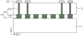
As shown in fig. 1-14, an embodiment of the present disclosure provides a semiconductor structure, comprising: an array semiconductor layer 1 having a plurality of memory blocks 3, the memory blocks 3 including a plurality of bit lines BL and a plurality of word lines WL; a peripheral semiconductor layer 2 bonded to the array semiconductor layer 1, the peripheral semiconductor layer 2 including a word line driving region 42 and a sense amplifying region 41; the sense amplifier 61 of the sense amplifying region 41 is electrically connected to the bit line BL, and the word line driver 62 of the word line driving region 42 is electrically connected to the word line WL; the orthographic projection of the word line driving region 42 and the sense amplifying region 41 on the array semiconductor layer 1 at least partially overlaps with the orthographic projection of the at least one memory block 3 on the array semiconductor layer 1.
Such a design has at least the following benefits:
first, the memory block 3 and peripheral devices such as the sense amplifier 61 and the word line driver 62 are provided on two different semiconductor layers, which is advantageous in reducing the area of a single semiconductor layer. Further, the space utilization of the semiconductor layer is improved in a direction perpendicular to the upper surface of the semiconductor layer. The memory block 3 and the peripheral devices are manufactured separately, so that the process is simpler, the production efficiency is higher, and the yield and the performance of the memory block 3 and the peripheral devices are improved.
Second, the orthographic projection of the word line driving region 42 and the sense amplifying region 41 on the array semiconductor layer 1 at least partially overlaps with the orthographic projection of the at least one memory block 3 on the array semiconductor layer 1. This is advantageous in reducing the distance between the bit line BL of the memory block 3 and the sense amplifier 61 and the distance between the word line WL of the memory block 3 and the word line driver 62, thereby shortening the wiring length and shortening the delay time.
The semiconductor structure will be described in detail with reference to the accompanying drawings.
The semiconductor structure comprises a first direction X, a second direction Y and a third direction Z, wherein the first direction X is perpendicular to the second direction Y, and the first direction X and the second direction Y are also perpendicular to the third direction Z. Wherein the first direction X and the second direction Y may be parallel to the upper surface of the array semiconductor layer 1, and the third direction Z may be perpendicular to the upper surface of the array semiconductor layer 1. The word line WL extends in the first direction X, and the bit line BL extends in the second direction Y.
Fig. 1 shows a cross-section of a semiconductor structure, and referring to fig. 1, the array semiconductor layer 1 and the peripheral semiconductor layer 2 may be both chip substrates or both wafers. The array semiconductor layer 1 and the peripheral semiconductor layer 2 may be connected together by hybrid bonding. The array semiconductor layer 1 and the peripheral semiconductor layer 2 may be bonded in a front-to-back or front-to-front manner. The side of the array semiconductor layer 1 on which the memory block 3 is formed is referred to as the front side, and the side of the peripheral semiconductor layer 2 on which the peripheral devices such as the sense amplifier 61 and the word line driver 62 are formed is referred to as the front side.
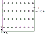
The semiconductor structure further comprises an interconnect structure 13, the interconnect structure 13 being for electrically connecting the array semiconductor layer 1 and the peripheral semiconductor layer 2. The interconnect structure 13 includes a first interconnect structure 11 located on the array semiconductor layer 1 and a second interconnect structure 12 located on the peripheral semiconductor layer 2. When the two semiconductor layers are bonded in a front-to-front manner, the first interconnect structure 11 may be a first pad, and the second interconnect structure 12 may be a second pad 122; when the two semiconductor layers are bonded in a front-to-back manner, the second interconnect structure 12 may include a second pad 122 and a conductive Via 121, and the conductive Via 121 may be a Through-Silicon Via (TSV). In addition, the peripheral semiconductor layer 2 is also formed with a data channel pad 123 (IO pad) connected to other circuits or devices.
Fig. 2 shows a schematic view of the bonding surface of the array semiconductor layer 1, fig. 3 shows a schematic view of the bonding surface of the peripheral semiconductor layer 2, and referring to fig. 2 to 3, pads are provided on the bonding surfaces of the array semiconductor layer 1 and the peripheral semiconductor layer 2 as the first interconnect structure 11 and the second interconnect structure 12, respectively. In some embodiments, the number of bit lines BL and the number of word lines WL of one memory block 3 may each be 900 to 1100, and the number of interconnection structures 13 may be equal to the sum of the numbers of bit lines BL and word lines WL. The area range of one storage block 3 may be 45 [ mu ] m×45 [ mu ] m to 55 [ mu ] m×55 [ mu ] m. Taking the number of the interconnection structures 13 as 2000 and the area of the memory block 3 as 50 μm×50 μm as an example, the pitch of the interconnection structures 13 is about 1.1118 μm, and the pitch meets the requirement of hybrid bonding.
Referring to fig. 4 to 12, the memory block 3 will be described in detail. The memory block 3 includes a plurality of memory cells arranged in an array, and the memory cells may include transistors and capacitors, and word lines WL may be connected to gates of the transistors, and bit lines BL may be connected to sources or drains of the transistors. In some embodiments, the memory block 3 may be a memory array (array), a memory bank (bank), and is correspondingly electrically connected to a global sense amplifier, a global word line driver. In other embodiments, the memory block 3 may be a memory array die (memory array tile, MAT) and is electrically connected to local sense amplifiers, local word line drivers.
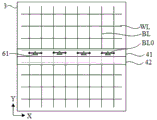
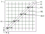
The word line driving region 42 may have a plurality of word line drivers 62 therein, and the word line drivers 62 may supply an on or off voltage to the word lines WL. The sense amplifying region 41 may have a plurality of sense amplifiers 61 therein, and the sense amplifiers 61 may amplify data transferred from the memory cells to the bit lines BL to ensure correct detection of the data stored in the memory cells. Referring to fig. 4-7, each word line driver 62 is electrically connected to one word line WL within the memory block 3. Referring to fig. 8 to 12, each sense amplifier 61 may be electrically connected to two bit lines BL within the memory block 3, and the sense amplifier 61 may amplify a voltage difference on the two bit lines BL. It should be noted that, the two bit lines BL electrically connected to the sense amplifier 61 may be located in the same memory block 3 or may be located in different memory blocks 3, which will be described in detail later.
The semiconductor structure further includes connection lines, and at least part of the connection lines may extend in a direction parallel to the upper surface of the array semiconductor layer 1, thereby changing the layout of the bit lines BL and the word lines WL, as an example. Specifically, referring to fig. 4, 6-7, the connection lines include a word line connection line WL0 located at the peripheral semiconductor layer 2, at least a portion of the word line connection line WL0 extends in the second direction Y, and the word line connection line WL0 is electrically connected to the word line driver 62 of the word line driving region 42 and is electrically connected to the word line WL through the interconnection structure 13. Referring to fig. 8 to 12, the connection lines include bit line connection lines BL0 at the peripheral semiconductor layer 2. At least a portion of the bit line connection line BL0 extends in the first direction X, and the bit line connection line BL0 is electrically connected to the sense amplifier 61 of the sense amplifying region 41 and to the bit line BL through the interconnect structure 13. That is, at least a portion of the bit line connection line BL0 is perpendicular to the bit line BL, and at least a portion of the word line connection line WL0 is perpendicular to the word line WL, so that the layout of the connection line can be standardized and the length of the connection line can be reduced.
The positional relationship of the word line driving region 42 and the sense amplifying region 41 will be described in detail below.
In some embodiments, referring to fig. 4-14, the extending direction of the word line driving region 42 and the extending direction of the sense amplifying region 41 are parallel to each other. This is because each memory block 3 has an electrical connection relationship with the word line driver 62 of the word line driving region 42 and the sense amplifier 61 of the sense amplifying region 41, and thus, arranging the extending directions of the two regions in parallel can simplify the layout of the connection lines and provide more sufficient space for other peripheral regions.
Specifically, referring to fig. 13 to 14, the word line driving region 42 and the sense amplifying region 41 are disposed adjacently, and both constitute a first peripheral region 412; the peripheral semiconductor layer 2 further includes a second peripheral region 43, and an address decoding circuit or a write driving circuit is included in the second peripheral region 43. In addition, the second peripheral region 43 may further include therein a decoder, an IO circuit, a clock signal generating circuit, and the like. The second peripheral region 43 is located at least on opposite sides of the first peripheral region 412. Thereby, the space of the second peripheral region 43 is larger, so that the process manufacturing can be facilitated and the signal interference can be reduced.
With continued reference to fig. 13-14, the peripheral semiconductor layer 2 also has a wiring layer 44 thereon to electrically connect the plurality of second peripheral regions 43. In some embodiments, a plurality of first peripheral regions 412 are spaced apart to reserve locations for routing layers 44 between second peripheral regions 43. The orthographic projection of at least part of the wiring layer 44 on the array semiconductor layer 1 may overlap with the orthographic projection of the space region of the adjacent memory block 3.
In other embodiments, the word line driving region 42 and the sense amplifying region 41 may be spaced apart from the sense amplifying region 41. The extending direction of the word line driving region 42 may also be different from the extending direction of the sense amplifying region 41, for example, the extending direction of the word line driving region 42 is perpendicular to the extending direction of the sense amplifying region 41.
In some embodiments, referring to fig. 5 to 7 and 9 to 12, the extending direction of the word line driving region 42 may be inclined with respect to the first direction X and the second direction Y, and the extending direction of the sense amplifying region 41 may be inclined with respect to the first direction X and the second direction Y. The inclined arrangement is beneficial to enlarging the overlapping area of the orthographic projection of the word line driving area 42 and the orthographic projection of the memory block 3 and the overlapping area of the orthographic projection of the sensing amplifying area 41 and the orthographic projection of the memory block 3, so that the process windows of the structures of the word line driver 62, the sensing amplifier 61, the connecting lines and the like can be enlarged to reduce the process difficulty. In addition, expanding the space of the sense amplifying region 41 and the word line driving region 42 is also advantageous in reducing parasitic capacitance, thereby improving the performance of the semiconductor structure.
For example, the extending direction of the word line driving region 42 may have an included angle with the first direction X and the second direction Y 60 degrees. The extending direction of the
 sensing amplifying region 41 may have an included angle of 30 ° to 60 ° with the first direction X and the second direction Y, respectively. With the included angle in the above range, a sufficient space can be provided for the word line driving region 42 and the sense amplifying region 41, and the position of the wiring layer 44 (refer to fig. 13 to 14) is prevented from being squeezed.
In other embodiments, referring to fig. 4 and 8, the extending direction of the word line driving region 42 may be parallel with respect to the first direction X or the second direction Y, and the extending direction of the sense amplifying region 41 may be parallel with respect to the first direction X or the second direction Y.
For example, the extending directions of the word line driving region 42 and the sense amplifying region 41 are all disposed in parallel in the first direction X, or the extending directions of the word line driving region 42 and the sense amplifying region 41 may be all disposed in parallel in the second direction Y. This ensures uniformity in the extending direction of the word line driving region 42 and the sense amplifying region 41.
In addition, the extending direction of the word line driving region 42 may also be parallel to the second direction Y, that is, parallel to the arrangement direction of the plurality of word lines WL; and the extending direction of the sense amplifying region 41 is parallel to the first direction X, i.e., parallel to the arrangement direction of the plurality of bit lines BL. In this way, the front projection of the word line driving region 42 on the array semiconductor layer 1 may at least partially overlap with the front projection of the plurality of word lines WL on the array semiconductor layer 1, and the front projection of the sense amplifying region 41 on the array semiconductor layer 1 may at least partially overlap with the front projection of the plurality of bit lines BL on the array semiconductor layer 1, which is advantageous for shortening the lengths of the bit line connection line BL0 and the word line connection line WL0.
Referring to fig. 4 to 7, the orthographic projection relationship and the electrical connection relationship of the word line driving region 42 and the memory block 3 will be exemplified. In order to more clearly illustrate the electrical connection relationship of the word line driver 62 and the memory block 3, fig. 4 to 7 do not illustrate the sense amplifier 61 and its electrical connection relationship with the memory block 3, and fig. 4 to 7 are all partial schematic views of the semiconductor structure. Note that, the orthographic projections described later refer to orthographic projections on the array semiconductor layer 1.
Referring to fig. 4-5, example one: the word line drivers 62 of the word line driving regions 42 are electrically connected to the memory blocks 3 in a one-to-one correspondence, and the orthographic projection of one word line driving region 42 on the array semiconductor layer 1 is located within the orthographic projection of the corresponding one memory block 3 on the array semiconductor layer 1. I.e. the orthographic projection relationship and the electrical connection relationship of the word line driving region 42 and the memory block 3 are one-to-one. The one-to-one correspondence is simpler, which is advantageous for reducing the distance between the word line WL and the word line driver 62, thereby improving the operation rate of the semiconductor structure.
Referring to fig. 4, the extending direction of the word line driving region 42 may be parallel to the first direction X or the second direction Y. Referring to fig. 5, the extending direction of the word line driving region 42 may also be inclined with respect to the first direction X and the second direction Y. That is, in example one, whether arranged in parallel or in an oblique arrangement, the front projection of the word line driving region 42 may overlap with the front projection of the memory block 3. As can be seen from comparing fig. 4-5, when obliquely arranged, the front projections of the plurality of word lines WL may have an overlapping relationship with the front projections of the word line driving regions 42, whereby the word line connection line WL0 may not be required to be arranged, or the word line connection line WL0 may be arranged to be shorter. Illustratively, the word line driving region 42 may extend in a diagonal direction of the memory block 3, which is advantageous in expanding the space of the word line driver 62 to reduce parasitic capacitance. In some embodiments, the orthographic projection of each word line WL has an overlapping relationship with the orthographic projection of one word line driver 62.
With continued reference to fig. 4-5, the orthographic projection of the word line driving region 42 on the array semiconductor layer 1 covers the center position of the orthographic projection of the memory block 3 on the array semiconductor layer 1. This can balance the layout of the word line connection line WL0 and reduce parasitic capacitance.
As shown in fig. 4, the memory block 3 may include two memory sub-blocks 31 arranged in the second direction Y, and the adjacent two word line drivers 62 may be electrically connected to the word lines WL of the different memory sub-blocks 31, whereby the word line connection lines WL0 corresponding to the adjacent two word line drivers 62 need not be disposed to face each other, thereby facilitating reduction of parasitic capacitance.
In other embodiments, referring to fig. 6 to 7, two adjacent memory blocks 3 arranged in the first direction X constitute a memory group 3a, or two adjacent memory blocks 3 arranged in the second direction Y constitute a memory group 3a; the front projection of a word line driving region 42 onto the array semiconductor layer 1 at least partially overlaps with the front projections of two memory blocks 3 of a memory group 3a onto the array semiconductor layer 1. Since the front projection of the word line driving region 42 can have an overlapping relationship with the front projections of the two memory blocks 3, it is advantageous to provide a more sufficient spatial position for the word line driver 62 to reduce signal interference and simplify the manufacturing process.
Specifically, referring to fig. 6, example two: the word line driving region 42 includes two connected first sub-regions 421, and the orthographic projections of the two first sub-regions 421 on the array semiconductor layer 1 at least partially overlap with orthographic projections of two different memory blocks 3 included in the corresponding memory group 3a on the array semiconductor layer 1, respectively; the word line drivers 62 of the two first sub-areas 421 are electrically connected to two different memory blocks 3, respectively.
For example, the two first sub-areas 421 are each electrically connected to the nearest one of the memory blocks 3. That is, the first sub-area 421 may have both the orthographic overlapping relationship and the electrical connection relationship with one memory block 3. This is advantageous in simplifying the layout of the word line connection WL0 and improving the signal transmission rate.
Specifically, each memory block 3 includes two memory sub-blocks 31, and the two memory sub-blocks 31 may be arranged in the first direction X or the second direction Y. The word line drivers 62 of the two first sub-areas 421 of the word line driving area 42 are respectively electrically connected with one memory sub-block 31 of the two different memory blocks 3, and the front projection of the first sub-area 421 at least partially overlaps with the front projection of the corresponding memory sub-block 31. That is, the word line driver 62 of one first sub-area 421 is electrically connected to the word line WL of one memory sub-block 31, and the front projection of one first sub-area 421 has an overlapping relationship with the front projection of one memory sub-block 31.
With continued reference to fig. 6, the plurality of word line drivers 62 in the first sub-area 421 may be arranged at equal intervals, and the lengths of the plurality of word line connection lines WL0 may be the same, so that uniformity of the semiconductor structure may be improved, and different delay times may be avoided. In addition, the plurality of word line connection lines WL0 may be arranged in a staggered manner, that is, the plurality of word line connection lines WL0 are not directly opposite to each other in the first direction X, so that parasitic capacitance may be reduced.
Referring to fig. 7, example three: the word line driving region 42 includes two connected first sub-regions 421, and the orthographic projections of the two first sub-regions 421 on the array semiconductor layer 1 at least partially overlap with orthographic projections of two different memory blocks 3 included in the corresponding memory group 3a on the array semiconductor layer 1, respectively; the word line drivers 62 of the two first sub-areas 421 are each electrically connected to one memory block 3 of the corresponding memory group 3 a. That is, although the orthographic projection of the word line driving region 42 may have an overlapping relationship with the orthographic projections of the two memory blocks 3, the word line driver 62 of the word line driving region 42 may be electrically connected to only one of the memory blocks 3.
It should be noted that, in the second and third examples, the extending direction of the word line driving region 42 may be inclined with respect to the first direction X and the second direction Y, that is, the extending direction of the word line driving region 42 is different from the first direction X and the second direction Y, so as to ensure that the word line driving region 42 may span across the two memory blocks 3.
As can be seen from the comparison examples two and three, when the word line driving region 42 and the word lines WL of the two memory blocks 3 are both in electrical connection, the length of the word line connection line WL0 is shorter, and the facing area between the word line connection lines WL0 is smaller, so that the delay time can be shortened, and the parasitic capacitance can be reduced.
Referring to fig. 8 to 12, the projected relationship and the electrical connection relationship of the sense amplifying region 41 and the memory block 3 will be exemplified. In order to more clearly illustrate the electrical connection of the sense amplifying region 41 to the memory block 3, fig. 8 to 12 do not illustrate the word line driver 62 and its electrical connection to the memory block 3. Fig. 8-12 are partial schematic views of semiconductor structures.
Referring to fig. 8-9, example four: the sense amplifiers 61 of the sense amplifying regions 41 are electrically connected to the memory blocks 3 in a one-to-one correspondence, and the orthographic projection of one sense amplifying region 41 on the array semiconductor layer 1 is located within the orthographic projection of the corresponding one memory block 3 on the array semiconductor layer 1. I.e. the orthographic projection relationship and the electrical connection relationship of the sense amplifying region 41 and the memory block 3 are both in one-to-one correspondence. The one-to-one connection is simple, and is beneficial to reducing the distance between the bit line BL and the sense amplifier 61, thereby improving the operation rate of the semiconductor structure.
Referring to fig. 8, the extension direction of the sense amplifying region 41 may be parallel to the first direction X or the second direction Y. Referring to fig. 9, the extending direction of the sense amplifying region 41 may be inclined with respect to the first direction X and the second direction Y. For example, the sense amplifying region 41 may extend in a direction of a diagonal line of the memory block 3, which is advantageous in expanding a space of the sense amplifying region 41 to reduce parasitic capacitance. In addition, the front projection of more bit lines BL may overlap with the front projection of the sense amplifying region 41 to simplify the layout of the bit line connection lines BL0.
With continued reference to fig. 8-9, the front projection of the sense amp region 41 onto the array semiconductor layer 1 covers the center position of the front projection of the memory block 3 onto the array semiconductor layer 1. This balances the layout of the bit line connection line BL0 and reduces parasitic capacitance.
Referring to fig. 8, the orthographic projection of the sense amplifier 61 may be located between orthographic projections of two bit lines BL electrically connected thereto, which is advantageous in reducing the length of the bit line connection line BL0. Further, referring to fig. 9, the sense amplifier 61 may also be located at the same side of two bit lines BL electrically connected thereto.
In other embodiments, referring to fig. 10 to 12, two adjacent memory blocks 3 arranged in the first direction X constitute a memory group 3a, or two adjacent memory blocks 3 arranged in the second direction Y constitute a memory group 3a; the front projection of a sense amplifier region 41 onto the array semiconductor layer 1 at least partially overlaps with the front projections of two memory blocks 3 of a memory group 3a onto the array semiconductor layer 1. Since the front projection of the sense amplifying region 41 may have an overlapping relationship with the front projections of the two memory blocks 3, it is advantageous to provide more sufficient spatial positions for the sense amplifying region 41 to reduce signal interference and simplify the manufacturing process.
Specifically, referring to fig. 10, example five: the sense amplifying region 41 includes two connected second sub-regions 411, and the orthographic projections of the two second sub-regions 411 on the array semiconductor layer 1 at least partially overlap with orthographic projections of two different memory blocks 3 included in the corresponding memory group 3a on the array semiconductor layer 1, respectively, and the sense amplifiers 61 of the two second sub-regions 411 are electrically connected to the two different memory blocks 3, respectively.
For example, the two second sub-areas 411 are electrically connected to the nearest one of the memory blocks 3, respectively. That is, the second sub-area 411 may have both the orthographic overlapping relationship and the electrical connection relationship with one memory block 3. This is advantageous for simplifying the layout of the bit line connection line BL0 and improving the signal transmission rate.
Specifically, each memory block 3 includes two memory sub-blocks 31, and the two memory sub-blocks 31 may be arranged in the first direction X or the second direction Y. The two second sub-areas 411 of the sense amplifying region 41 are respectively and electrically connected with one memory sub-block 31 of the two different memory blocks 3, and the front projection of the second sub-area 411 at least partially overlaps with the front projection of the corresponding memory sub-block 31. That is, the sense amplifier 61 of one second sub-region 411 is electrically connected to the bit line BL of one memory sub-block 31, and the front projection of one second sub-region 411 has an overlapping relationship with the front projection of the corresponding one memory sub-block 31.
Referring to fig. 11, example six: the sense amplifying region 41 includes two connected second sub-regions 411, and the orthographic projections of the two second sub-regions 411 on the array semiconductor layer 1 at least partially overlap with orthographic projections of two different memory blocks 3 included in the corresponding memory group 3a on the array semiconductor layer 1, respectively, and the sense amplifiers 61 of the two second sub-regions 411 are electrically connected to one memory block 3 in the corresponding memory group 3. That is, although the front projection of the sense amplifying region 41 may have an overlapping relationship with the front projections of the two memory blocks 3, the sense amplifier 61 of the sense amplifying region 41 may be electrically connected to only one of the memory blocks 3.
As is clear from the comparison examples five and six, when the sense amplifying region 41 and the bit lines BL of the two memory blocks 3 are electrically connected, the length of the bit line connection lines BL0 is shorter, and the facing area between the bit line connection lines BL0 is smaller, so that the delay time can be shortened, and the parasitic capacitance can be reduced.
Referring to fig. 12, example seven: the sense amplifier 61 of one sense amplifying region 41 is electrically connected to two memory blocks 3 in the corresponding memory group 3 a. I.e. one sense amp region 41 and all bit lines BL in both memory blocks 3 with an orthographic overlapping relationship therewith.
For example, two memory blocks 3 of the memory group 3a are arranged in the second direction Y. Each sense amplifier 61 is electrically connected to the bit lines BL of two different memory blocks 3, and the two bit lines BL electrically connected to the same sense amplifier 61 are aligned in the second direction Y. This can reduce the number of sense amplifiers 61, thereby providing more sufficient space for the peripheral devices of the second peripheral region 43 and the structures of the wiring layer 44 (refer to fig. 13 to 14) and the like.
It should be noted that, in examples five to seven, the extending direction of the sense amplifying region 41 may be inclined with respect to the first direction X and the second direction Y, that is, the extending direction of the sense amplifying region 41 is different from the first direction X and the second direction Y, to ensure that the sense amplifying region 41 may span across the two memory blocks 3.
It should be noted that, without contradiction, the "orthographic projection relationship, electrical connection relationship of the word line driving region 42 and the memory block 3" may be combined with the "orthographic projection relationship, electrical connection relationship of the sense amplifying region 41 and the memory block 3".
For example, a word line driving region 42 and a sense amplifying region 41 each have a orthographic projection overlapping relationship and an electrical connection relationship with a memory block 3. Alternatively, a word line driving region 42 and a sense amplifying region 41 each have a orthographic projection overlapping relationship and an electrical connection relationship with the two memory blocks 3. This advantageously increases the uniformity of the semiconductor structure and advantageously reduces the length of the connection lines, thereby providing more room for the second peripheral region 43. It should be noted that the embodiments of the present disclosure are not limited to the two combinations described above. That is, the respective schemes of example one to example three may be combined two by two with the respective schemes of example four to example seven.
In summary, in the embodiment of the disclosure, the memory block 3 and the peripheral device are disposed on two different semiconductor layers and bonded, so that the area of the semiconductor layers is reduced, and the production efficiency and the performance of the semiconductor structure are improved. The orthographic projection of the word line driving region 42 and the sense amplifying region 41 on the array semiconductor layer 1 at least partially overlaps with the orthographic projection of the at least one memory block 3 on the array semiconductor layer 1, which is advantageous in reducing the length of the connection line and shortening the delay time.
The embodiments of the present disclosure also provide a memory including the semiconductor structure provided in the foregoing embodiments, and reference may be made to the foregoing embodiments for a detailed description of the semiconductor structure. The Memory may be a dynamic Random Access Memory (Dynamic Random Access Memory, DRAM), a Static Random-Access Memory (SRAM), a high bandwidth Memory (High Bandwidth Memory, HBM), or the like.
The embodiments of the present disclosure also provide a method for manufacturing a semiconductor structure, which may manufacture the semiconductor structure provided in the foregoing embodiments, and reference may be made to the foregoing embodiments for a detailed description of the semiconductor structure.
Referring to fig. 1, the manufacturing method includes: an array semiconductor layer 1 is provided and a first interconnect structure 11 is formed on the array semiconductor layer 1. Illustratively, the first pads are formed as the first interconnect structures 11 by a patterning process and a deposition process. The array semiconductor layer 1 may further have a dielectric layer, and an upper surface of the first interconnection structure 11 may be flush with an upper surface of the dielectric layer. The array semiconductor layer further has a plurality of memory blocks 3 (refer to fig. 4 to 14), and the memory blocks 3 include a plurality of bit lines BL and a plurality of word lines WL.
A peripheral semiconductor layer 2 is provided and a second interconnect structure 12 is formed on the peripheral semiconductor layer 2. Illustratively, the second pads 122 and the conductive vias 121 are formed as the second interconnect structure 12 by a patterning process and a deposition process. In other embodiments, only the second pad 122 may be formed as the second interconnect structure 12. The peripheral semiconductor layer 2 may further have a dielectric layer, and the upper surface of the second interconnect structure 12 may be flush with the upper surface of the dielectric layer. The peripheral semiconductor layer 2 further includes a word line driving region 42 and a sense amplifying region 41.
The array semiconductor layer 1 and the peripheral semiconductor layer 2 are bonded through the first interconnect structure 11 and the second interconnect structure 12 such that the orthographic projection of the word line driving region 42 and the sense amplifying region 41 on the array semiconductor layer 1 at least partially overlaps with the orthographic projection of the at least one memory block 3 on the array semiconductor layer 1, and such that the sense amplifier 61 of the sense amplifying region 41 is electrically connected to the bit line BL and the word line driver 62 of the word line driving region 42 is electrically connected to the word line WL. Illustratively, hybrid bonding is employed such that the first interconnect structure 11 is aligned and bonded with the second interconnect structure 12 such that the dielectric layer on the array semiconductor layer 1 is aligned and bonded with the dielectric layer on the peripheral semiconductor layer 2.
In other embodiments, the bonding of the two semiconductor layers may also be achieved by means of fusion bonding. That is, the first interconnect structure 11 and the second interconnect structure 12 may each be a solder ball protruding from the surface of the semiconductor layer.
In the description of the present specification, a description of the terms "some embodiments," "exemplary," and the like, means that a particular feature, structure, material, or characteristic described in connection with the embodiment or example is included in at least one embodiment or example of the present disclosure. In this specification, schematic representations of the above terms are not necessarily directed to the same embodiment or example. Furthermore, the particular features, structures, materials, or characteristics described may be combined in any suitable manner in any one or more embodiments or examples. Furthermore, the different embodiments or examples described in this specification and the features of the different embodiments or examples may be combined and combined by those skilled in the art without contradiction.
While embodiments of the present disclosure have been shown and described above, it should be understood that the above embodiments are illustrative and not to be construed as limiting the present disclosure, and that variations, modifications, alternatives, and variations may be made to the above embodiments by those of ordinary skill in the art within the scope of the present disclosure, which is therefore intended to be within the scope of the present disclosure as defined by the claims and specification.
Claims (15)
1. A semiconductor structure, comprising:
an array semiconductor layer having a plurality of memory blocks including a plurality of bit lines and a plurality of word lines;
a peripheral semiconductor layer bonded to the array semiconductor layer, the peripheral semiconductor layer including a word line driving region and a sense amplifying region; a sense amplifier of the sense amplifying region is electrically connected with the bit line, and a word line driver of the word line driving region is electrically connected with the word line;
the orthographic projection of the word line driving region and the sense amplifying region on the array semiconductor layer at least partially overlaps with the orthographic projection of at least one memory block on the array semiconductor layer.
2. The semiconductor structure of claim 1, wherein,
the word line drivers of the word line driving areas are electrically connected with the memory blocks in a one-to-one correspondence, and the orthographic projection of one word line driving area on the array semiconductor layer is positioned in the orthographic projection of the corresponding memory block on the array semiconductor layer; and/or the number of the groups of groups,
the sense amplifiers of the sense amplifying regions are electrically connected with the memory blocks in a one-to-one correspondence, and the orthographic projection of one sense amplifying region on the array semiconductor layer is positioned in the orthographic projection of the corresponding memory block on the array semiconductor layer.
3. The semiconductor structure of claim 2, wherein the word line extends in a first direction and the bit line extends in a second direction, the first direction being perpendicular to the second direction;
an extending direction of the word line driving region is inclined with respect to the first direction and the second direction; and/or the number of the groups of groups,
the extending direction of the sense amplifying region is inclined with respect to the first direction and the second direction.
4. The semiconductor structure of claim 3, wherein,
the included angle between the extending direction of the word line driving area and the first direction and the second direction is 30-60 degrees; and/or the number of the groups of groups,
the extending direction of the sensing amplifying region and the included angle between the first direction and the second direction are 30-60 degrees respectively.
5. The semiconductor structure of claim 4, wherein an orthographic projection of the word line driving region and/or the sense amplifying region on the array semiconductor layer covers a center position of an orthographic projection of the memory block on the array semiconductor layer.
6. The semiconductor structure of claim 2, wherein,
the word lines extend in a first direction, the bit lines extend in a second direction, and the first direction is perpendicular to the second direction;
the extending direction of the word line driving region is parallel to the first direction or the second direction, and/or the extending direction of the sense amplifying region is parallel to the first direction or the second direction.
7. The semiconductor structure of claim 1, wherein,
two adjacent storage blocks arranged in a first direction form a storage group, or two adjacent storage blocks arranged in a second direction form a storage group;
the orthographic projection of one said word line driving region on said array semiconductor layer at least partially overlaps with orthographic projections of two said memory blocks of one said memory group on said array semiconductor layer; and/or the number of the groups of groups,
the front projection of one sensing amplifying region on the array semiconductor layer is at least partially overlapped with the front projection of two memory blocks of one memory group on the array semiconductor layer.
8. The semiconductor structure of claim 7, wherein,
the word lines extend in the first direction, the bit lines extend in the second direction, and the first direction is perpendicular to the second direction;
an extending direction of the word line driving region is inclined with respect to the first direction and the second direction; and/or the number of the groups of groups,
the extending direction of the sense amplifying region is inclined with respect to the first direction and the second direction.
9. The semiconductor structure of claim 8, wherein,
the word line driving area comprises two connected first subareas, and the orthographic projections of the two first subareas on the array semiconductor layer are respectively overlapped with orthographic projections of two different memory blocks included in the corresponding memory group on the array semiconductor layer at least partially;
the word line drivers of the two first sub-regions are electrically connected to two different memory blocks, respectively, or the word line drivers of the two first sub-regions are electrically connected to one memory block in the corresponding memory group.
10. The semiconductor structure of claim 8, wherein,
the sensing amplifying region comprises two connected second sub-regions, and the orthographic projections of the two second sub-regions on the array semiconductor layer are respectively overlapped with orthographic projections of two different memory blocks included in the corresponding memory group on the array semiconductor layer at least partially;
the sense amplifiers of the two second sub-regions are electrically connected to two different memory blocks, respectively, or the sense amplifiers of the two second sub-regions are electrically connected to a corresponding one of the memory blocks in the memory group.
11. The semiconductor structure of any of claims 1-10, wherein,
the extending direction of the word line driving region and the extending direction of the sense amplifying region are parallel to each other.
12. The semiconductor structure of claim 11, wherein,
the word line driving area and the sensing amplifying area are adjacently arranged, and the word line driving area and the sensing amplifying area form a first peripheral area; the peripheral semiconductor layer further includes a second peripheral region including an address decoding circuit or a write driving circuit therein, the second peripheral region being located at least on opposite sides of the first peripheral region.
13. The semiconductor structure of any of claims 1-10, wherein the semiconductor structure further comprises:
an interconnect structure for electrically connecting the array semiconductor layer and the peripheral semiconductor layer;
a bit line connection line located at the peripheral semiconductor layer, at least a portion of the bit line connection line extending in a first direction, the bit line connection line being electrically connected to the sense amplifier of the sense amplifying region and electrically connected to the bit line through the interconnection structure;
and a word line connection line positioned on the peripheral semiconductor layer, at least part of the word line connection line extending along the second direction, the word line connection line being electrically connected with the word line driver of the word line driving region and electrically connected with the word line through the interconnection structure.
14. A memory, comprising: the semiconductor structure of any one of claims 1-13.
15. A method of forming a semiconductor structure, comprising:
providing an array semiconductor layer and forming a first interconnection structure on the array semiconductor layer, wherein the array semiconductor layer is provided with a plurality of memory blocks, and the memory blocks comprise a plurality of bit lines and a plurality of word lines;
providing a peripheral semiconductor layer and forming a second interconnection structure on the peripheral semiconductor layer, the peripheral semiconductor layer including a word line driving region and a sense amplifying region;
bonding the array semiconductor layer and the peripheral semiconductor layer through the first interconnect structure and the second interconnect structure such that orthographic projections of the word line driving region and the sense amplifying region on the array semiconductor layer at least partially overlap orthographic projections of at least one of the memory blocks on the array semiconductor layer, and electrically connecting sense amplifiers of the sense amplifying region with the bit lines, and word line drivers of the word line driving region are electrically connected with the word lines.
Priority Applications (1)
| Application Number | Priority Date | Filing Date | Title |
|---|---|---|---|
| CN202310463781.7A CN116189727B (en) | 2023-04-26 | 2023-04-26 | Semiconductor structure, memory and manufacturing method of semiconductor structure |
Applications Claiming Priority (1)
| Application Number | Priority Date | Filing Date | Title |
|---|---|---|---|
| CN202310463781.7A CN116189727B (en) | 2023-04-26 | 2023-04-26 | Semiconductor structure, memory and manufacturing method of semiconductor structure |
Publications (2)
| Publication Number | Publication Date |
|---|---|
| CN116189727A true CN116189727A (en) | 2023-05-30 |
| CN116189727B CN116189727B (en) | 2023-09-19 |
Family
ID=86444633
Family Applications (1)
| Application Number | Title | Priority Date | Filing Date |
|---|---|---|---|
| CN202310463781.7A Active CN116189727B (en) | 2023-04-26 | 2023-04-26 | Semiconductor structure, memory and manufacturing method of semiconductor structure |
Country Status (1)
| Country | Link |
|---|---|
| CN (1) | CN116189727B (en) |
Citations (12)
| Publication number | Priority date | Publication date | Assignee | Title |
|---|---|---|---|---|
| US5768174A (en) * | 1995-12-06 | 1998-06-16 | Samsung Electronics Co., Ltd. | Integrated circuit memory devices having metal straps to improve word line driver reliability |
| JP2003059289A (en) * | 2001-06-04 | 2003-02-28 | Toshiba Corp | Semiconductor memory |
| US20110169062A1 (en) * | 2010-01-08 | 2011-07-14 | Elpida Memory, Inc. | Semiconductor device and method of fabricating the same |
| US20140246725A1 (en) * | 2013-03-04 | 2014-09-04 | Samsung Electronics Co., Ltd. | Integrated Circuit Memory Devices Including Parallel Patterns in Adjacent Regions |
| CN110890372A (en) * | 2018-09-07 | 2020-03-17 | 三星电子株式会社 | Semiconductor memory device and method of manufacturing the same |
| CN112599528A (en) * | 2020-12-14 | 2021-04-02 | 武汉新芯集成电路制造有限公司 | Semiconductor device and method for manufacturing the same |
| CN114121968A (en) * | 2020-08-25 | 2022-03-01 | 三星电子株式会社 | Three-dimensional semiconductor memory device |
| CN114747009A (en) * | 2020-01-28 | 2022-07-12 | 桑迪士克科技有限责任公司 | Joint assembly with vertical power and control signal connections adjacent to sense amplifier region and method of forming same |
| CN115410617A (en) * | 2022-09-19 | 2022-11-29 | 长鑫存储技术有限公司 | Word line driver and memory device |
| US20230055147A1 (en) * | 2021-08-17 | 2023-02-23 | Samsung Electronics Co., Ltd. | Semiconductor memory device |
| US20230060149A1 (en) * | 2021-08-31 | 2023-03-02 | Yangtze Memory Technologies Co., Ltd. | Memory devices having vertical transistors and methods for forming the same |
| CN115995248A (en) * | 2021-10-20 | 2023-04-21 | 爱思开海力士有限公司 | Memory device and method of operating the same |
-
2023
- 2023-04-26 CN CN202310463781.7A patent/CN116189727B/en active Active
Patent Citations (12)
| Publication number | Priority date | Publication date | Assignee | Title |
|---|---|---|---|---|
| US5768174A (en) * | 1995-12-06 | 1998-06-16 | Samsung Electronics Co., Ltd. | Integrated circuit memory devices having metal straps to improve word line driver reliability |
| JP2003059289A (en) * | 2001-06-04 | 2003-02-28 | Toshiba Corp | Semiconductor memory |
| US20110169062A1 (en) * | 2010-01-08 | 2011-07-14 | Elpida Memory, Inc. | Semiconductor device and method of fabricating the same |
| US20140246725A1 (en) * | 2013-03-04 | 2014-09-04 | Samsung Electronics Co., Ltd. | Integrated Circuit Memory Devices Including Parallel Patterns in Adjacent Regions |
| CN110890372A (en) * | 2018-09-07 | 2020-03-17 | 三星电子株式会社 | Semiconductor memory device and method of manufacturing the same |
| CN114747009A (en) * | 2020-01-28 | 2022-07-12 | 桑迪士克科技有限责任公司 | Joint assembly with vertical power and control signal connections adjacent to sense amplifier region and method of forming same |
| CN114121968A (en) * | 2020-08-25 | 2022-03-01 | 三星电子株式会社 | Three-dimensional semiconductor memory device |
| CN112599528A (en) * | 2020-12-14 | 2021-04-02 | 武汉新芯集成电路制造有限公司 | Semiconductor device and method for manufacturing the same |
| US20230055147A1 (en) * | 2021-08-17 | 2023-02-23 | Samsung Electronics Co., Ltd. | Semiconductor memory device |
| US20230060149A1 (en) * | 2021-08-31 | 2023-03-02 | Yangtze Memory Technologies Co., Ltd. | Memory devices having vertical transistors and methods for forming the same |
| CN115995248A (en) * | 2021-10-20 | 2023-04-21 | 爱思开海力士有限公司 | Memory device and method of operating the same |
| CN115410617A (en) * | 2022-09-19 | 2022-11-29 | 长鑫存储技术有限公司 | Word line driver and memory device |
Also Published As
| Publication number | Publication date |
|---|---|
| CN116189727B (en) | 2023-09-19 |
Similar Documents
| Publication | Publication Date | Title |
|---|---|---|
| US10885946B2 (en) | Stacked DRAM device and method of manufacture | |
| CN111292784B (en) | Integrated assembly comprising vertical stacking layers | |
| US7808804B2 (en) | Power line layout | |
| KR20130053278A (en) | Semiconductor device for increasing bitline contact area and module and system using the device | |
| US10163497B2 (en) | Three dimensional dual-port bit cell and method of using same | |
| KR20220042932A (en) | Semiconductor device and electronic system | |
| CN111211126B (en) | Three-dimensional memory and forming method thereof | |
| CN116189727B (en) | Semiconductor structure, memory and manufacturing method of semiconductor structure | |
| US11925027B2 (en) | Three-dimensional memory device including sense amplifiers having a common width and separation | |
| TWI783814B (en) | Memory device and preparation method thereof | |
| US8766324B2 (en) | Power line layout techniques for integrated circuits having modular cells | |
| CN114783481A (en) | Integrated assembly | |
| TW202223723A (en) | Semiconductor device and fabrication method thereof | |
| TW202316306A (en) | Storage device and manufacturing method thereof | |
| CN114765038A (en) | Integrated assembly and semiconductor memory device | |
| US6317358B1 (en) | Efficient dual port DRAM cell using SOI technology | |
| US20060013056A1 (en) | Memory architecture | |
| KR20210088810A (en) | Three dimensional semiconductor memory device | |
| US20240130131A1 (en) | Vertical memory device | |
| WO2023097907A1 (en) | Semiconductor structure and method for preparing same | |
| WO2022228281A1 (en) | Three-dimensional memory, chip packaging structure, and electronic device | |
| US11031405B2 (en) | Peripheral logic circuits under DRAM memory arrays | |
| JP3865753B2 (en) | Manufacturing method of semiconductor integrated circuit device | |
| CN114420180A (en) | Dynamic random access memory and forming method thereof | |
| CN117766003A (en) | Memory and memory system |
Legal Events
| Date | Code | Title | Description |
|---|---|---|---|
| PB01 | Publication | ||
| PB01 | Publication | ||
| SE01 | Entry into force of request for substantive examination | ||
| SE01 | Entry into force of request for substantive examination | ||
| GR01 | Patent grant | ||
| GR01 | Patent grant |