CN115691965A - Coil component - Google Patents
Coil component Download PDFInfo
- Publication number
- CN115691965A CN115691965A CN202210852213.1A CN202210852213A CN115691965A CN 115691965 A CN115691965 A CN 115691965A CN 202210852213 A CN202210852213 A CN 202210852213A CN 115691965 A CN115691965 A CN 115691965A
- Authority
- CN
- China
- Prior art keywords
- coil
- planar
- inner end
- planar coil
- insulating substrate
- Prior art date
- Legal status (The legal status is an assumption and is not a legal conclusion. Google has not performed a legal analysis and makes no representation as to the accuracy of the status listed.)
- Pending
Links
- 239000004020 conductor Substances 0.000 claims abstract description 55
- 230000000149 penetrating effect Effects 0.000 claims abstract description 5
- 239000000758 substrate Substances 0.000 claims description 60
- 239000011810 insulating material Substances 0.000 claims description 12
- 230000017525 heat dissipation Effects 0.000 abstract description 8
- 239000012212 insulator Substances 0.000 description 25
- 229920005989 resin Polymers 0.000 description 15
- 239000011347 resin Substances 0.000 description 15
- 239000006247 magnetic powder Substances 0.000 description 12
- 239000002184 metal Substances 0.000 description 11
- 229910052751 metal Inorganic materials 0.000 description 11
- 239000003822 epoxy resin Substances 0.000 description 5
- 229920000647 polyepoxide Polymers 0.000 description 5
- 239000000843 powder Substances 0.000 description 5
- 238000009713 electroplating Methods 0.000 description 4
- 239000000463 material Substances 0.000 description 3
- 230000002093 peripheral effect Effects 0.000 description 3
- 229910045601 alloy Inorganic materials 0.000 description 2
- 239000000956 alloy Substances 0.000 description 2
- 239000011230 binding agent Substances 0.000 description 2
- 239000011521 glass Substances 0.000 description 2
- 239000002245 particle Substances 0.000 description 2
- 238000000206 photolithography Methods 0.000 description 2
- 238000007747 plating Methods 0.000 description 2
- XEEYBQQBJWHFJM-UHFFFAOYSA-N Iron Chemical compound [Fe] XEEYBQQBJWHFJM-UHFFFAOYSA-N 0.000 description 1
- 229910001030 Iron–nickel alloy Inorganic materials 0.000 description 1
- 239000004642 Polyimide Substances 0.000 description 1
- 239000004840 adhesive resin Substances 0.000 description 1
- 229920006223 adhesive resin Polymers 0.000 description 1
- 239000004760 aramid Substances 0.000 description 1
- 229920003235 aromatic polyamide Polymers 0.000 description 1
- 230000001413 cellular effect Effects 0.000 description 1
- 239000000919 ceramic Substances 0.000 description 1
- 230000007423 decrease Effects 0.000 description 1
- 230000003247 decreasing effect Effects 0.000 description 1
- 238000010586 diagram Methods 0.000 description 1
- 230000000694 effects Effects 0.000 description 1
- 239000004744 fabric Substances 0.000 description 1
- 230000020169 heat generation Effects 0.000 description 1
- 230000001771 impaired effect Effects 0.000 description 1
- 239000000696 magnetic material Substances 0.000 description 1
- 238000000034 method Methods 0.000 description 1
- 239000011812 mixed powder Substances 0.000 description 1
- 238000005192 partition Methods 0.000 description 1
- 229910000889 permalloy Inorganic materials 0.000 description 1
- 229920001721 polyimide Polymers 0.000 description 1
- 229910000702 sendust Inorganic materials 0.000 description 1
- 229920001187 thermosetting polymer Polymers 0.000 description 1
Images


Classifications
-
- H—ELECTRICITY
- H01—ELECTRIC ELEMENTS
- H01F—MAGNETS; INDUCTANCES; TRANSFORMERS; SELECTION OF MATERIALS FOR THEIR MAGNETIC PROPERTIES
- H01F27/00—Details of transformers or inductances, in general
- H01F27/28—Coils; Windings; Conductive connections
- H01F27/2847—Sheets; Strips
-
- H—ELECTRICITY
- H01—ELECTRIC ELEMENTS
- H01F—MAGNETS; INDUCTANCES; TRANSFORMERS; SELECTION OF MATERIALS FOR THEIR MAGNETIC PROPERTIES
- H01F17/00—Fixed inductances of the signal type
- H01F17/0006—Printed inductances
- H01F17/0013—Printed inductances with stacked layers
-
- H—ELECTRICITY
- H01—ELECTRIC ELEMENTS
- H01F—MAGNETS; INDUCTANCES; TRANSFORMERS; SELECTION OF MATERIALS FOR THEIR MAGNETIC PROPERTIES
- H01F17/00—Fixed inductances of the signal type
- H01F17/04—Fixed inductances of the signal type with magnetic core
-
- H—ELECTRICITY
- H01—ELECTRIC ELEMENTS
- H01F—MAGNETS; INDUCTANCES; TRANSFORMERS; SELECTION OF MATERIALS FOR THEIR MAGNETIC PROPERTIES
- H01F27/00—Details of transformers or inductances, in general
- H01F27/08—Cooling; Ventilating
- H01F27/22—Cooling by heat conduction through solid or powdered fillings
-
- H—ELECTRICITY
- H01—ELECTRIC ELEMENTS
- H01F—MAGNETS; INDUCTANCES; TRANSFORMERS; SELECTION OF MATERIALS FOR THEIR MAGNETIC PROPERTIES
- H01F27/00—Details of transformers or inductances, in general
- H01F27/28—Coils; Windings; Conductive connections
- H01F27/2876—Cooling
-
- H—ELECTRICITY
- H01—ELECTRIC ELEMENTS
- H01F—MAGNETS; INDUCTANCES; TRANSFORMERS; SELECTION OF MATERIALS FOR THEIR MAGNETIC PROPERTIES
- H01F27/00—Details of transformers or inductances, in general
- H01F27/28—Coils; Windings; Conductive connections
- H01F27/32—Insulating of coils, windings, or parts thereof
- H01F27/324—Insulation between coil and core, between different winding sections, around the coil; Other insulation structures
-
- H—ELECTRICITY
- H01—ELECTRIC ELEMENTS
- H01F—MAGNETS; INDUCTANCES; TRANSFORMERS; SELECTION OF MATERIALS FOR THEIR MAGNETIC PROPERTIES
- H01F17/00—Fixed inductances of the signal type
- H01F17/0006—Printed inductances
- H01F17/0013—Printed inductances with stacked layers
- H01F2017/002—Details of via holes for interconnecting the layers
-
- H—ELECTRICITY
- H01—ELECTRIC ELEMENTS
- H01F—MAGNETS; INDUCTANCES; TRANSFORMERS; SELECTION OF MATERIALS FOR THEIR MAGNETIC PROPERTIES
- H01F17/00—Fixed inductances of the signal type
- H01F17/04—Fixed inductances of the signal type with magnetic core
- H01F2017/048—Fixed inductances of the signal type with magnetic core with encapsulating core, e.g. made of resin and magnetic powder
-
- H—ELECTRICITY
- H01—ELECTRIC ELEMENTS
- H01F—MAGNETS; INDUCTANCES; TRANSFORMERS; SELECTION OF MATERIALS FOR THEIR MAGNETIC PROPERTIES
- H01F27/00—Details of transformers or inductances, in general
- H01F27/28—Coils; Windings; Conductive connections
- H01F27/29—Terminals; Tapping arrangements for signal inductances
-
- H—ELECTRICITY
- H01—ELECTRIC ELEMENTS
- H01F—MAGNETS; INDUCTANCES; TRANSFORMERS; SELECTION OF MATERIALS FOR THEIR MAGNETIC PROPERTIES
- H01F27/00—Details of transformers or inductances, in general
- H01F27/28—Coils; Windings; Conductive connections
- H01F27/32—Insulating of coils, windings, or parts thereof
- H01F27/327—Encapsulating or impregnating
Abstract
The invention provides a coil component, which realizes the improvement of heat dissipation of the periphery of a through conductor. In the coil component, the sectional area of the inner end of the planar coil is designed to be relatively large, so that heat generated in the penetrating conductor is easily transmitted to the inner end. In this way, in the coil member, heat is efficiently transferred from the through conductor to the inner end portion, and therefore, high heat dissipation can be achieved around the through conductor.
Description
Technical Field
The present invention relates to a coil component.
Background
Conventionally, a coil component in which a plurality of coils are provided in an element body is known. Patent document 1 below discloses a four-terminal coil component in which two coils are provided in an element body, and planar coils provided on both surfaces of an insulating substrate are connected to each other via a through conductor.
Documents of the prior art
Patent document
Patent document 1: japanese patent laid-open publication No. 2015-130472
Disclosure of Invention
Problems to be solved by the invention
In the above-described coil component, the temperature around the through conductor may become excessively high during driving, and in this case, the stability of the element characteristics may be impaired. The inventors have made extensive studies on heat dissipation through the periphery of a conductor, and have newly found a technique capable of improving heat dissipation.
The invention aims to provide a coil component which improves heat dissipation of the periphery of a through conductor.
Means for solving the problems
In a coil component according to an aspect of the present invention, the coil component includes: an element body; an insulating substrate disposed within the element; and a pair of coil portions each including a pair of planar coils wound in parallel with each other on the insulating substrate and a pair of through conductors overlapping with inner end portions of the planar coils adjacent to each other and penetrating through the insulating substrate, wherein a sectional area of the inner end portion of the planar coil is larger than a sectional area of the planar coil at an outer portion than the inner end portion and is larger than a sectional area of the through conductor in a cross section orthogonal to the insulating substrate.
In the coil component, the cross-sectional area of the through conductor is relatively small, and the through conductor is likely to generate heat because the current density of the current flowing through the planar coil during driving is high. However, since the sectional area of the inner end of the planar coil overlapping the through conductor is larger than the sectional area of the planar coil outside thereof, heat generated in the through conductor is easily transmitted to the inner end. In this way, in the coil member, heat is efficiently transferred from the through conductor to the inner end portion, and therefore, high heat dissipation can be achieved around the through conductor.
In the coil component according to another aspect of the present invention, the height of the inner end of the planar coil is lower than the height of the planar coil at the outer portion than the inner end.
In the coil component according to another aspect of the present invention, the width of the inner end of the planar coil is larger than the width of the planar coil in the outer portion than the inner end.
In the coil component according to the other aspect of the present invention, the planar coil is covered with an insulating material, and the thickness of the insulating material covering the inner end of the planar coil is larger than the thickness of the insulating material covering the planar coil at the outer portion than the inner end.
In the coil component of another aspect of the present invention, the thickness of the insulating substrate is smaller than the thickness of the inner end of the planar coil.
In the coil component according to another aspect of the present invention, the inner end portions of the pair of planar coils have different thicknesses.
In a coil component according to another aspect of the present invention, a thickness of the insulating substrate is smaller than a dimension of the through conductor in an extending direction of the insulating substrate.
In a coil component according to another aspect of the present invention, a cross-sectional shape of the through conductor in a cross section perpendicular to the insulating substrate is formed in a slender shape.
In the coil component according to another aspect of the present invention, the through conductor is biased to the outside with respect to the inner end of the planar coil.
Effects of the invention
According to the present invention, a coil component is provided in which heat dissipation is improved around a through conductor.
Drawings
Fig. 1 is a schematic perspective view of a coil component according to an embodiment.
Fig. 2 is a diagram showing the inside of the coil component of fig. 1.
Fig. 3 is an exploded view of the coil shown in fig. 2.
Fig. 4 is a sectional view taken along line IV-IV of the coil component shown in fig. 2.
Fig. 5 is a sectional view taken along line V-V of the coil component shown in fig. 2.
Fig. 6 is a top view of the coil shown in fig. 2.
Fig. 7 is an enlarged view of a main portion of the sectional view shown in fig. 4.
Detailed Description
Embodiments of the present invention will be described in detail below with reference to the drawings. In the description, the same reference numerals are used for the same elements or elements having the same functions, and redundant description is omitted.
As an example, the coil component 1 of the embodiment is a balanced-unbalanced coil. The balun coil is utilized when, for example, a near field wireless communication circuit (NFC circuit) is mounted on a cellular terminal. And converting the unbalanced signal of the antenna and the balanced signal of the NFC circuit through the balanced-unbalanced coil to realize the connection of the unbalanced circuit and the balanced circuit. The coil component 1 can also be used for a common mode filter or a transformer.
As shown in fig. 1, the coil component 1 includes an element body 10, a coil structure 20 embedded in the element body 10, and two pairs of external terminal electrodes 60A, 60B, 60C, and 60D provided on the surface of the element body 10.
The element body 10 has a rectangular parallelepiped shape and has six faces 10a to 10f. For example, the element body 10 is designed to have a long side of 2.0mm, a short side of 1.25mm, and a height of 0.65 mm. In the planes 10a to 10f of the element body 10, the end face 10a (1 st end face) and the end face 10b (2 nd end face) are parallel to each other, the upper face 10c and the lower face 10d are parallel to each other, and the side face 10e and the side face 10f are parallel to each other. The upper surface 10c of the element body 10 is a surface facing in parallel to the mounting surface of the mounting board on which the coil component 1 is mounted.
The element body 10 is composed of a metal-containing magnetic powder resin 12 as one of magnetic materials. The metal-containing magnetic powder resin 12 is a bonding powder in which metal magnetic powder is bonded by a bonding resin. The metal magnetic powder containing the metal magnetic powder resin 12 is composed of, for example, an iron-nickel alloy (permalloy), carbonyl iron, an amorphous, amorphous or crystalline fesicricon alloy, an sendust alloy, or the like. The adhesive resin is, for example, a thermosetting epoxy resin. In the present embodiment, the content of the metal magnetic powder in the binder powder is 80 to 92vol% in terms of volume percentage and 95 to 99wt% in terms of mass percentage. From the viewpoint of magnetic properties, the content of the metal magnetic powder in the binder powder may be 85 to 92vol% by volume and 97 to 99wt% by mass. The magnetic powder containing the metal magnetic powder resin 12 may be a powder having one average particle diameter or a mixed powder having a plurality of average particle diameters.
The metal-containing magnetic powder resin 12 of the element body 10 integrally covers a coil structure 20 described later. Specifically, the metal-containing magnetic powder resin 12 covers the coil structure 20 from the top-bottom direction, and covers the outer periphery of the coil structure 20. In addition, the metal-containing magnetic powder resin 12 fills the inner peripheral region of the coil structure 20.
The coil structure 20 includes an insulating substrate 30, an upper coil structure 40A provided on the insulating substrate 30, and a lower coil structure 40B provided on the insulating substrate 30.
The insulating substrate 30 is designed to have a flat plate shape, extends between the end faces 10a, 10b of the element body 10, and is orthogonal to the end faces 10a, 10 b. The insulating substrate 30 extends parallel to the upper surface 10c and the lower surface 10d of the element body 10. As shown in fig. 3, the insulating substrate 30 includes an elliptical ring-shaped coil forming portion 31 extending in the longitudinal direction of the element assembly 10, and a pair of frame portions 34A and 34B extending in the transverse direction of the element assembly 10 and sandwiching the coil forming portion 31 from both sides. An elliptical opening 32 extending in the longitudinal direction of the element body 10 is provided in the central portion of the coil forming portion 31.
The insulating substrate 30 is made of a nonmagnetic insulating material. The thickness of the insulating substrate 30 may be designed to be in the range of 10 to 60 μm, for example. In the present embodiment, the insulating substrate 30 has a structure in which an epoxy resin is impregnated in a glass cloth. The resin constituting the insulating substrate 30 is not limited to epoxy resin, and BT resin, polyimide, aramid, or the like may be used. The insulating substrate 30 may be made of ceramic or glass. The material constituting the insulating substrate 30 may be a printed substrate material produced in large quantities. The insulating substrate 30 may be made of a resin material used for a BT printed circuit board, an FR4 printed circuit board, or an FR5 printed circuit board.
The upper coil structure 40A is provided on the substrate upper surface 30A of the coil forming portion 31 of the insulating substrate 30. As shown in fig. 2 and 3, the upper coil structure 40A includes a 1 st planar coil 41, a 2 nd planar coil 42, and an upper insulator 50A. The 1 st planar coil 41 and the 2 nd planar coil 42 are wound on the upper surface 30a of the insulating substrate 30 in a state of being adjacent to each other in parallel.
The 1 st planar coil 41 is a substantially oval spiral air-core coil wound around the opening 32 of the coil forming portion 31 in the same layer on the upper surface 30a of the insulating substrate 30. The number of turns of the 1 st planar coil 41 may be 1 turn or may be plural turns. In the present embodiment, the number of turns of the 1 st planar coil 41 is 3 to 4. The 1 st planar coil 41 has an outer end 41a and an inner end 41b. The outer end 41a is provided on the frame 34A and is exposed from the end face 10a of the element body 10. The inner end 41b is provided at the edge of the opening 32. A 1 st through conductor 41c extending in the thickness direction of the insulating substrate 30 is provided on the insulating substrate 30 so as to penetrate the insulating substrate 30 at a position overlapping the inner end 41b of the 1 st planar coil 41. The 1 st planar coil 41 is made of, for example, cu, and can be formed by electrolytic plating.
Similarly to the 1 st planar coil 41, the 2 nd planar coil 42 is a substantially oval spiral air-core coil wound around the opening 32 of the coil forming portion 31 on the upper surface 30a of the insulating substrate 30 in the same layer. The 2 nd planar coil 42 is wound on the inner peripheral side of the 1 st planar coil 41 so as to be adjacent to the 1 st planar coil 41. The number of turns of the 2 nd planar coil 42 may be 1 turn or may be plural turns. In the present embodiment, the number of turns of the 2 nd planar coil 42 is the same as that of the 1 st planar coil 41. The 2 nd planar coil 42 has an outer end 42a and an inner end 42b. Like the outer end 41a of the 1 st planar coil 41, the outer end 42a of the 2 nd planar coil 42 is provided on the frame 34A and exposed from the end face 10a of the element body 10. The inner end 42b of the 2 nd planar coil 42 is disposed at the edge of the opening 32, and is adjacent to the inner end 41b of the 1 st planar coil 41. A 2 nd through conductor 42c extending in the thickness direction of the insulating substrate 30 is provided on the insulating substrate 30 so as to penetrate through the insulating substrate 30 at a position overlapping with the inner end 42b of the 2 nd planar coil 42. The 2 nd through conductor 42c is adjacent to the 1 st through conductor 41c. Like the 1 st planar coil 41, the 2 nd planar coil 42 is made of, for example, cu, and can be formed by electrolytic plating.
The upper insulator 50A is provided on the upper surface 30A of the insulating substrate 30. The upper insulator 50A includes a thick film resist patterned by known photolithography. The thick film resist of the upper insulator 50A demarcates the plating growth areas of the 1 st planar coil 41 and the 2 nd planar coil 42. In the present embodiment, as shown in fig. 4, the upper insulator 50A integrally covers the 1 st planar coil 41 and the 2 nd planar coil 42, more specifically, covers the side surfaces and the upper surface of the 1 st planar coil 41 and the 2 nd planar coil 42. In the present embodiment, the upper insulator 50A includes an insulating resin film covering the upper surfaces of the 1 st and 2 nd planar coils 41 and 42. As shown in fig. 5 and 6, a part of the upper insulator 50A extends from the inside of the element body 10 to the end face 10A of the element body 10 through between the outer end 41a and the outer end 42a, and is exposed at the end face 10A. As shown in fig. 5 and 6, a part of the upper insulator 50A extends from the inside of the element body 10 to the end face 10b along the substrate upper surface 30A and is exposed at the end face 10 b. The thickness of the upper insulator 50A is thicker than the thickness of the 1 st and 2 nd planar coils 41 and 42. The upper insulator 50A is made of, for example, epoxy resin.
The lower coil structure 40B is provided on the substrate lower surface 30B of the coil forming portion 31 of the insulating substrate 30. As shown in fig. 2 and 3, the lower coil structure 40B includes a 1 st planar coil 41, a 2 nd planar coil 42, and a lower insulator 50B. The 1 st planar coil 41 and the 2 nd planar coil 42 are wound on the lower surface 30b of the insulating substrate 30 in a state of being adjacent to each other in parallel.
The 1 st and 2 nd planar coils 41 and 42 of the lower coil structure 40B have symmetry with the 1 st and 2 nd planar coils 41 and 42 of the upper coil structure 40A. More specifically, the 1 st and 2 nd planar coils 41 and 42 of the lower coil structure 40B have a shape in which the 1 st and 2 nd planar coils 41 and 42 of the upper coil structure 40A are inverted around an axis parallel to the short sides of the element body 10.
The outer end 41a of the 1 st planar coil 41 of the lower coil structure 40B is provided in the frame 34B and is exposed from the end face 10B of the element body 10. The inner end 41B of the 1 st planar coil 41 of the lower coil structure 40B overlaps the 1 st through conductor 41c provided on the insulating substrate 30. Therefore, the inner end 41B of the 1 st planar coil 41 of the lower coil structure 40B is electrically connected to the inner end 41B of the 1 st planar coil 41 of the upper coil structure 40A via the 1 st through conductor 41c. The 1 st planar coil 41 of the lower coil structure 40B is made of, for example, cu, and can be formed by electrolytic plating.
The outer end 42a of the 2 nd planar coil 42 of the lower coil structure 40B is provided in the frame 34B and is exposed from the end face 10B of the element body 10. The inner end 42B of the 2 nd planar coil 42 of the lower coil structure 40B overlaps the 2 nd penetrating conductor 42c provided on the insulating substrate 30. Therefore, the inner end 42B of the 2 nd planar coil 42 of the lower coil structure 40B is electrically connected to the inner end 42B of the 2 nd planar coil 42 of the upper coil structure 40A via the 2 nd through conductor 42c. The 2 nd planar coil 42 of the lower coil structure 40B is made of, for example, cu, and can be formed by electrolytic plating.
The lower insulator 50B is provided on the lower surface 30B of the insulating substrate 30. The lower insulator 50B includes a thick film resist patterned by known photolithography. Like the thick film resist of the upper insulator 50A, the thick film resist of the lower insulator 50B partitions the plating growth regions of the 1 st planar coil 41 and the 2 nd planar coil 42. In the present embodiment, as shown in fig. 4, the lower insulator 50B integrally covers the 1 st and 2 nd planar coils 41 and 42, more specifically, the side and upper surfaces of the 1 st and 2 nd planar coils 41 and 42. In the present embodiment, the lower insulator 50B includes an insulating resin film covering the upper surfaces of the 1 st and 2 nd planar coils 41 and 42. Similarly to the upper insulator 50A, a part of the lower insulator 50B extends from the inside of the element body 10 to the end face 10B of the element body 10 through between the outer end 41a and the outer end 42a, and is exposed at the end face 10B. A part of the lower insulator 50B extends from the inside of the element body 10 to the end face 10a along the board lower surface 30B, and is exposed at the end face 10 a. The thickness of the lower insulator 50B is thicker than the thickness of the 1 st and 2 nd planar coils 41 and 42. The thickness of the lower insulator 50B may be the same as that of the upper insulator 50A. The lower insulator 50B is made of, for example, epoxy resin.
The element body 10 includes a pair of coil portions C1 and C2 constituting a double coil structure. The 1 st coil portion C1 includes a 1 st planar coil 41 provided on the upper coil structure 40A of the upper surface 30A of the insulating substrate 30, a 1 st planar coil 41 provided on the lower coil structure 40B of the lower surface 30B of the insulating substrate 30, and a 1 st through conductor 41C connecting the 1 st planar coils 41 on both surfaces to each other. In the 1 st coil part C1, the outer end 41a of the 1 st planar coil 41 of the upper coil structure 40A constitutes the 1 st end, and the outer end 41a of the 1 st planar coil 41 of the lower coil structure 40B constitutes the 2 nd end. The 2 nd coil portion C2 is constituted by a 2 nd planar coil 42 provided on the upper coil structure 40A of the upper surface 30A of the insulating substrate 30, a 2 nd planar coil 42 provided on the lower coil structure 40B of the lower surface 30B of the insulating substrate 30, and a 2 nd through conductor 42C connecting the 2 nd planar coils 42 on both surfaces to each other. In the 2 nd coil part C2, the outer end 42a of the 2 nd planar coil 42 of the upper coil structure 40A constitutes the 1 st end, and the outer end 42a of the 2 nd planar coil 42 of the lower coil structure 40B constitutes the 2 nd end.
The two pairs of external terminal electrodes 60A, 60B, 60C, and 60D are provided in a pair on the end faces 10A and 10B of the element body 10, which are parallel to each other.
Of the pair of external terminal electrodes 60A and 60B provided on the end face 10A, the external terminal electrode 60A is connected to the outer end 41a of the 1 st planar coil 41 of the upper coil structure 40A, and the external terminal electrode 60B is connected to the outer end 42a of the 2 nd planar coil 42 of the upper coil structure 40A. As shown in fig. 6, the external terminal electrode 60A is biased toward the side surface 10f and covers the end surface 10A in the vicinity of the side surface 10f when viewed from the end surface 10A. The external terminal electrode 60B is biased toward the side surface 10e and covers the end surface 10a in the vicinity of the side surface 10 e. The external terminal electrode 60A and the external terminal electrode 60B are separated by a predetermined uniform width when viewed from the end face 10A side.
Of the pair of external terminal electrodes 60C and 60D provided on the end face 10B, the external terminal electrode 60C is connected to the outer end 41a of the 1 st planar coil 41 of the lower coil structure 40B, and the external terminal electrode 60D is connected to the outer end 42a of the 2 nd planar coil 42 of the lower coil structure 40B. The external terminal electrode 60C is biased toward the side surface 10f and covers the end surface 10b in the vicinity of the side surface 10f. The external terminal electrode 60D is biased toward the side surface 10e and covers the end surface 10b in the vicinity of the side surface 10 e. The external terminal electrode 60C and the external terminal electrode 60D are separated by a predetermined uniform width when viewed from the end face 10b side.
The external terminal electrode 60A on the end face 10A and the external terminal electrode 60C on the end face 10b are provided at positions corresponding to each other in the longitudinal direction of the element body 10. Similarly, the external terminal electrode 60B on the end face 10a and the external terminal electrode 60D on the end face 10B are provided at positions corresponding to each other in the longitudinal direction of the element body 10.
The external terminal electrodes 60A, 60B, 60C, 60D are each bent in an L shape, and continuously cover the end faces 10A, 10B and the upper surface 10C. In the present embodiment, the external terminal electrodes 60A, 60B, 60C, and 60D are made of resin electrodes, for example, made of a resin containing Ag powder.
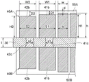
Next, the structures of the inner ends 41b and 42b and the through conductors 41c and 42c of the planar coils 41 and 42 will be described with reference to fig. 7. Fig. 7 is a cross section perpendicular to the insulating substrate 30, that is, a cross section passing through the through conductors 41c and 42c, and is an enlarged view of a main portion of the cross section of fig. 4. In the following description, the configurations of the planar coils 41 and 42 in the upper coil structure 40A will be described, but the configurations of the planar coils 41 and 42 in the lower coil structure 40B are also the same or similar.
As shown in fig. 7, the sectional area S1 of the inner end 41b of the 1 st planar coil 41 and the sectional area S2 of the inner end 42b of the 2 nd planar coil 42 are both designed to be larger than the sectional area S of the planar coils 41, 42 of turns outside the inner ends 41b, 42b. In the embodiment shown in fig. 7, the width W1 of the inner end 41b of the 1 st planar coil 41 and the width W2 of the inner end 42b of the 2 nd planar coil 42 are both larger than the width W of the planar coils 41, 42 having turns outside the inner ends 41b, 42b. In the embodiment shown in fig. 7, both the thickness D1 of the insulating material covering the portion of the 1 st planar coil 41 at the inner end 41b and the thickness D2 of the insulating material covering the portion of the 2 nd planar coil 42 at the inner end 42b are greater than the thickness D of the insulating material covering the portions of the planar coils 41 and 42 on the outer turns than the inner ends 41b and 42b.
The sectional area S1 of the inner end 41b of the 1 st planar coil 41 and the sectional area S2 of the inner end 42b of the 2 nd planar coil 42 are designed to be different from each other. The cross-sectional areas S1, S2 may also be designed to be identical. In the embodiment shown in fig. 7, the sectional area S1 of the inner end 41b of the 1 st planar coil 41 is larger than the sectional area S2 of the inner end 42b of the 2 nd planar coil 42. In addition, the thickness H1 of the inner end 41b of the 1 st planar coil 41 and the thickness H2 of the inner end 42b of the 2 nd planar coil 42 are designed to be different from each other. In the embodiment shown in fig. 7, the thickness H1 of the inner end 41b of the 1 st planar coil 41 is thicker than the thickness H2 of the inner end 42b of the 2 nd planar coil 42. Regarding the thickness of the upper insulator 50A, the thickness D1 of the insulating material in the portion covering the inner end 41b of the 1 st planar coil 41 is thinner than the thickness D2 of the insulating material in the portion covering the inner end 42b of the 2 nd planar coil 42. The thicknesses D1 and D2 may be the same. The width W1 of the inner end 41b of the 1 st planar coil 41 may be different from the width W2 of the inner end 42b of the 2 nd planar coil 42, or may be the same as the width W2 of the inner end 42b of the 2 nd planar coil 42.
The 1 st through conductor 41c overlapping the inner end 41b of the 1 st planar coil 41 and the 2 nd through conductor 42c overlapping the inner end 42b of the 2 nd planar coil 42 have the same thickness as the thickness t of the insulating substrate 30. The 1 st and 2 nd through conductors 41c and 42c have circular cross sections in the thickness direction of the insulating substrate 30. The thickness of the insulating substrate 30 is designed to be thinner than the diameters of the 1 st and 2 nd through conductors 41c and 42c (i.e., the dimension in the extending direction of the insulating substrate 30). The sectional area S1 of the 1 st through conductor 41c is smaller than the sectional area S1 of the inner end 41b of the 1 st planar coil 41. The cross-sectional area S2 of the 2 nd penetrating conductor 42c is smaller than the cross-sectional area S2 of the inner end 42b of the 2 nd planar coil 42. The 1 st through conductor 41c and the 2 nd through conductor 42c each have a cross-sectional shape formed in a slender waist shape, and have a width that decreases from the upper and lower surfaces 30a and 30b of the insulating substrate 30 toward the inside. Further, the 1 st and 2 nd through conductors 41c, 42c are both biased on the outer peripheral side of the coils (right side in fig. 7) with respect to the inner ends 41b, 42b of the planar coils 41, 42. The 1 st and 2 nd through conductors 41c, 42c may be positioned not on the outer periphery of the coil (for example, positioned with respect to the center positions of the inner ends 41b, 42 b).
As described above, the cross-sectional areas S1 and S2 of the through conductors 41c and 42c are relatively small (for example, smaller than the cross-sectional areas S1 and S2 of the inner ends 41b and 42b of the planar coils 41 and 42), and the current density of the current flowing through the planar coils 41 and 42 when the coil component 1 is driven becomes high in the through conductors 41c and 42c, so that heat is likely to be generated in the through conductors 41c and 42c. In particular, when the through conductors 41c and 42c are adjacent to each other as in the coil component 1, excessive heat generation is likely to occur. When the cross-sectional shape of the through conductors 41c and 42c is a slender shape, the current density is high, and heat is easily generated.
In the coil component 1, the sectional areas S1 and S2 of the inner ends 41b and 42b of the planar coils 41 and 42 are designed to be relatively large (for example, larger than the sectional area S of the planar coils 41 and 42 on the outer side thereof), so that heat generated in the through conductors 41c and 42c is easily transmitted to the inner ends 41b and 42b. In this way, in the coil component 1, since heat is efficiently transferred from the through conductors 41c, 42c to the inner end portions 41b, 42b, high heat dissipation is achieved around the through conductors 41c, 42c.
The present invention is not limited to the above-described embodiments, and various embodiments can be adopted.
For example, the number of turns of the 1 st coil part and the number of turns of the 2 nd coil part can be increased or decreased as appropriate. In addition, three or more coil parts may be included in the element body of the coil part.
Claims (9)
1. A coil component, comprising:
an element body;
an insulating substrate disposed within the element; and
a pair of coil sections each including a pair of planar coils wound in parallel with each other on the insulating substrate and a pair of through conductors each overlapping an inner end of the planar coil adjacent to each other and penetrating the insulating substrate,
in a cross section orthogonal to the insulating substrate, a cross sectional area of an inner end of the planar coil is larger than a cross sectional area of a portion of the planar coil located outside the inner end and larger than a cross sectional area of the through conductor.
2. The coil component of claim 1, wherein:
the height of the inner end of the planar coil is lower than the height of the planar coil at the outer side of the inner end.
3. A coil component as claimed in claim 1 or 2, wherein:
the width of the inner end of the planar coil is larger than the width of the planar coil at the outer side of the inner end.
4. The coil component according to any one of claims 1 to 3, wherein:
the planar coil is covered with an insulating material, and the thickness of the insulating material covering the inner end of the planar coil is greater than the thickness of the insulating material covering the portion of the planar coil outside the inner end.
5. The coil component according to any one of claims 1 to 4, wherein:
the thickness of the insulating substrate is smaller than that of the inner end of the planar coil.
6. The coil component according to any one of claims 1 to 5, wherein:
the inner end portions of the pair of planar coils have different thicknesses.
7. The coil component according to any one of claims 1 to 6, wherein:
the thickness of the insulating substrate is smaller than the dimension of the through conductor in the extending direction of the insulating substrate.
8. The coil component according to any one of claims 1 to 7, wherein:
the cross-sectional shape of the through conductor in a cross section orthogonal to the insulating substrate is a slender waist shape.
9. A coil component as claimed in any one of claims 1 to 8, wherein:
the through conductor is biased to the outside with respect to the inner end of the planar coil.
Applications Claiming Priority (2)
| Application Number | Priority Date | Filing Date | Title |
|---|---|---|---|
| JP2021120283A JP2023016158A (en) | 2021-07-21 | 2021-07-21 | Coil component |
| JP2021-120283 | 2021-07-21 |
Publications (1)
| Publication Number | Publication Date |
|---|---|
| CN115691965A true CN115691965A (en) | 2023-02-03 |
Family
ID=84977521
Family Applications (1)
| Application Number | Title | Priority Date | Filing Date |
|---|---|---|---|
| CN202210852213.1A Pending CN115691965A (en) | 2021-07-21 | 2022-07-20 | Coil component |
Country Status (3)
| Country | Link |
|---|---|
| US (1) | US20230022189A1 (en) |
| JP (1) | JP2023016158A (en) |
| CN (1) | CN115691965A (en) |
Families Citing this family (1)
| Publication number | Priority date | Publication date | Assignee | Title |
|---|---|---|---|---|
| JP7287216B2 (en) * | 2019-09-24 | 2023-06-06 | Tdk株式会社 | coil structure |
-
2021
- 2021-07-21 JP JP2021120283A patent/JP2023016158A/en active Pending
-
2022
- 2022-07-18 US US17/866,837 patent/US20230022189A1/en active Pending
- 2022-07-20 CN CN202210852213.1A patent/CN115691965A/en active Pending
Also Published As
| Publication number | Publication date |
|---|---|
| US20230022189A1 (en) | 2023-01-26 |
| JP2023016158A (en) | 2023-02-02 |
Similar Documents
| Publication | Publication Date | Title |
|---|---|---|
| US9812247B2 (en) | Electronic component | |
| US10607769B2 (en) | Electronic component including a spacer part | |
| CN105810386B (en) | Electronic assembly | |
| CN115691965A (en) | Coil component | |
| CN111243836A (en) | Inductance element and electronic device | |
| CN112786282B (en) | Inductor | |
| US20230022095A1 (en) | Coil component | |
| US20220392698A1 (en) | Coil component | |
| US20230023284A1 (en) | Coil component | |
| JP4600638B2 (en) | Coil parts | |
| US20230063602A1 (en) | Coil component | |
| US20220415566A1 (en) | Electronic component | |
| US20230063586A1 (en) | Coil component | |
| US20230066655A1 (en) | Coil component | |
| CN112908606B (en) | Coil component | |
| US20230072929A1 (en) | Coil component | |
| JP2019175942A (en) | Surface mounting inductor and manufacturing method thereof | |
| US20210166859A1 (en) | Coil component | |
| US20230290561A1 (en) | Multilayer coil component | |
| KR102130679B1 (en) | Chip electronic component | |
| US20230230742A1 (en) | Multilayer coil component | |
| CN114628125A (en) | Coil component | |
| KR20200074074A (en) | Chip electronic component | |
| JP2022126115A (en) | Laminated coil component | |
| CN115985619A (en) | Coil component |
Legal Events
| Date | Code | Title | Description |
|---|---|---|---|
| PB01 | Publication | ||
| PB01 | Publication | ||
| SE01 | Entry into force of request for substantive examination | ||
| SE01 | Entry into force of request for substantive examination |